EP1220364A2 - Anschlussleiter und Verfahren zur M ontierung eines Anschlussleiters auf einer Leiterplatte - Google Patents
Anschlussleiter und Verfahren zur M ontierung eines Anschlussleiters auf einer Leiterplatte Download PDFInfo
- Publication number
- EP1220364A2 EP1220364A2 EP01130120A EP01130120A EP1220364A2 EP 1220364 A2 EP1220364 A2 EP 1220364A2 EP 01130120 A EP01130120 A EP 01130120A EP 01130120 A EP01130120 A EP 01130120A EP 1220364 A2 EP1220364 A2 EP 1220364A2
- Authority
- EP
- European Patent Office
- Prior art keywords
- contact
- connecting terminal
- fixed
- side wall
- contact part
- Prior art date
- Legal status (The legal status is an assumption and is not a legal conclusion. Google has not performed a legal analysis and makes no representation as to the accuracy of the status listed.)
- Granted
Links
Images


Classifications
-
- H—ELECTRICITY
- H01—ELECTRIC ELEMENTS
- H01R—ELECTRICALLY-CONDUCTIVE CONNECTIONS; STRUCTURAL ASSOCIATIONS OF A PLURALITY OF MUTUALLY-INSULATED ELECTRICAL CONNECTING ELEMENTS; COUPLING DEVICES; CURRENT COLLECTORS
- H01R13/00—Details of coupling devices of the kinds covered by groups H01R12/70 or H01R24/00 - H01R33/00
- H01R13/02—Contact members
- H01R13/22—Contacts for co-operating by abutting
- H01R13/24—Contacts for co-operating by abutting resilient; resiliently-mounted
- H01R13/2442—Contacts for co-operating by abutting resilient; resiliently-mounted with a single cantilevered beam
Definitions
- the invention relates a terminal to be connected onto a circuit board (hereinafter referred to as connecting terminal) and a method of mounting the same onto the circuit board, particularly to a connecting terminal which is effective in cases where the circuit board is grounded to another circuit board, sealing plate, a chassis, a case frame, and the like so as to prevent an electromagnetic field produced from a high frequency circuit used in a portable telephone and the like from influencing upon other devices, and a method of mounting the connecting terminal onto the circuit board.
- a connecting terminal which is effective in cases where the circuit board is grounded to another circuit board, sealing plate, a chassis, a case frame, and the like so as to prevent an electromagnetic field produced from a high frequency circuit used in a portable telephone and the like from influencing upon other devices, and a method of mounting the connecting terminal onto the circuit board.
- a grounding terminal has been already known since it has been disclosed, e.g., in Japanese Patent No. 3, 068, 557 and Japanese Utility Model Registration No. 3, 064, 756, wherein a grounding terminal is mounted onto a circuit board, i.e., printed circuit board and it comes into compression contact with a grounding conductor, thereby grounding the printed circuit board.
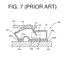
- Figs. 6 and 7 show a grounding terminal as disclosed in Japanese Patent No. 3, 068, 557, wherein Fig. 6 is a plan view showing a state where the grounding terminal is mounted onto a printed-circuit board, and Fig. 7 is a side sectional view taken along the line A'-A' in Fig 6. In Fig.
- grounding terminal 400 designated by 100 is a grounding terminal, 140 a contact part, 141 a restriction part, 160 a wall-like part, 161 a pawl part, 300 a printed-circuit board, 250a, 250b conductive patterns, 260 a soft solder, and 400 a grounding conductor.
- the grounding conductor 400 is omitted in Fig. 6.
- the grounding terminal 100 is formed by bending a thin strip metal member.
- a junction part 120 to be joined to the printed-circuit board 300 is provided on the metal member at substantially the center thereof in the longitudinal direction.
- the metal member is bent at the junction part 120 in the longitudinal direction so that it has a shape of mountain in cross section and a groove is formed in one surface of the junction part 120.
- Two junction faces 120a, 120b are formed on both sides of the mountain.
- the groove is formed in the junction part 120 at the portion remote from the central position thereof in the longitudinal direction by a given interval so that one junction face 120a is smaller than the other junction face 120b.
- the metal member is bent at both ends of the junction part 120 in a direction opposite to the junction faces 120a, 120b.
- One end of the metal member which is bent at both ends of the junction part 120 is folded back at the end of the junction part 120 to form the contact part 140 and the restriction part 141.
- the contact part 140 comes into compression contact with the grounding conductor 400 and elastically deformed about a folded back part, namely, turnup part 130 by a given amount in a state where the grounding terminal is soldered to the printed-circuit board 300.
- Fig. 7 shows a state where the contact part 140 comes into compression contact with the grounding conductor 400 and is elastically deformed.
- a state where the contact part 140 does not come into contact with a grounding conductor 400 is illustrated by two-dotted one chain line.
- the contact part 140 comes into compression contact with the grounding conductor 400 by a repulsive force caused by the elastic deformation thereof and becomes conductive to the grounding conductor 400 so that the printed-circuit board 300 is grounded to the
- the restriction part 141 is formed on the grounding terminal 100 while continuously connecting to the contact part 140 of the grounding terminal 100 so that the contact part 140 does not exceed an elastic limit when the contact part 140 is elastically deformed.
- the restriction part 141 comes into contact with the opposite side of the junction face of the junction part 120 at its tip end when the contact part 140 is elastically deformed by a given amount so that the amount of elastic deformation of the contact part 140 is restricted.
- the tip end of the restriction part 141 comes into contact with the opposite side of the junction part 120 every time the contact part 140 comes into compression contact with the grounding conductor 400, there arises a possibility that the opposite side of the junction part 120 with which the restriction part 141 comes into contact is injured to induce inferior connection at the junction part 120. Further, since the tip end of the restriction part 141 comes into contact with the opposite side of the junction face when the contact part 140 comes into compression contact with the grounding conductor 400, the moving range of the contact part 140 is restricted, thereby making it difficult to obtain a repulsive force owing to the elastic deformation of the contact part 140, namely, to obtain a given contact pressure between the grounding conductor 400 and the contact part 140.
- the turnup part 130 about which the contact part 140 is elastically deformed is formed at a position remote from the junction part 120 having a small junction area by a given interval.
- a solder 260a supplied to the junction face120a having a small junction area is not sucked up to the turnup part 130 of the contact part 140, thereby preventing the solder 260a from sticking to the turnup part 130.
- the turnup part 130 is formed at the position remote from the small junction face120a having a small junction area by a given interval, the contact part 140 is to be formed in a specific shape, causing a problem in the formation of the contact part 140.
- the solder 260a is stuck to the portion close to the turnup part 130, a peeling force is applied to the solder fixed part every time the contact part 140 is elastically deformed. If the contact part 140 is repeatedly elastically deformed, the solder fixed part is peeled off and cracked, thereby making it difficult to maintain the conduction.
- Fig. 8 shows a grounding terminal disclosed in Japanese Utility Model Registration No. 3,064,756.
- the grounding terminal comprises a substrate part which is mounted on a grounding pattern of a printed-circuit board 350, a spring contact 311 which is protruded integrally from one side of the substrate part to a side confronting the substrate part, and an engaging wall 360 integrally standing upright on the substrate part and engaging with the tip end of the spring contact 311. Since the grounding terminal has the engaging wall 360 engaging with the tip end of the spring contact 311, the engaging wall 360 functions as a stopper relative to an irregular external force which is produced when fingers and the like strike against the spring contact 311, thereby restraining the deformation of the grounding terminal.
- the spring contact 311 is not irregularly deformed.
- the sealed panel and the like is pressed down or compressed oblique or in the lateral direction, which is caused by the deviation of the sealed panel, the spring contact 311 is crushed in the lateral direction and is irregularly deformed, so that there arises a possibility that an elastic force as designed cannot be maintained.
- the grounding terminal is designed such that the portion where the spring contact 311 actually contacts the sealed panel and the like has an allowable width in a movable (swingable) range of the spring contact 311 at a position higher than the tip end of the engaging wall even if the grounding terminal is rendered in a state where it contacts the sealed panel and the like in the same manner as rendered in a state where it does not contact the sealed panel and the like.
- the spring contact 311 having such a construction is excessively pressed down by a sealed panel and the like, the tip end of the contact comes into contact with the substrate part, and hence the movable range is limited, making it difficult to keep an optimum elastic force.
- the connecting terminal is made of a substantially strip conductive plate and comprises a fixed part provided at one end of the conductive plate to be mounted onto a circuit board, and a contact part extended from the fixed part and formed by bending the conductive plate toward the fixed part to form a curved part, said contact part being elastically deformed about the curved part to come into compression contact with a substantially flat conductor, wherein the connecting terminal is characterized in further comprising a pair of side wall parts formed by bending the conductive plate at the fixed part in a width direction thereof, said side wall parts having a height to an extent to restrict excessive deformation of the contact part when the contact part comes into compression contact with the flat conductor.
- the connecting terminal of the invention is characterized in that an interval between the side wall parts is made larger than a width of the contact part, and both end sides of the contact part contact or approach inner side walls of the side wall parts when the contact part comes into compression contact with the flat conductor.
- the connecting terminal can allow the circuit board to come into compression contact with the flat conductor with certainty. Particularly, even if the contact part comes into compression contact with the flat conductor oblique or in the lateral direction, the contact part will not irregularly deformed so that an optimum contact pressure can be maintained.
- the connecting terminal of the invention is characterized in further comprising projection pieces provided on the conductive plate in the width direction close to the curved part between the fixed part and the curved part. If the connecting terminal is mounted onto the circuit board, the projection pieces come into contact with the circuit board, thereby realizing stable mounting.
- a connecting terminal is made of a substantially strip conductiveplate and comprises a fixed part provided at one end of the conductive plate to be mounted onto a circuit board, and a contact part extended from the fixed part and formed by bending the conductive plate toward the fixed part to form a curved part, said contact part being elastically deformed about the curved part to come into compression contact with a substantially flat conductor, wherein the connecting terminal is characterized in further comprising a notch defined and separating between the fixed part and the curved part, said fixed part and the separated part being connected to each other by a pair of side wall parts formed by bending the conductive plate in the width direction thereof toward the contact part.
- the connecting terminal of the invention is characterized in that a plurality of notches are defined in the fixed part for cutting off the fixed part into a plurality of fixed parts and separated part, said fixed parts and the separated part being connected to each other by a pair of side wall parts formed by bending the fixed part in the width direction thereof toward the contact part.
- the connecting terminal of the invention is characterized in that the side wall parts have a height to an extent to restrict excessive deformation of the contact part when the contact part comes into compression contact with the flat conductor.
- the connecting terminal of the invention is characterized in that the interval between the side wall parts is larger than a width of the contact part, and both end sides of the contact part contact or approach inner surfaces of the side wall parts when the contact part comes into compression contact with the flat conductor.
- the connecting terminal of the invention is characterized in further comprising projection pieces provided on the conductive plate in the width direction close to the curved part between the fixed part and the curved part.
- the method of mounting a connecting terminal onto a conductor of a circuit board according to the invention is characterized in comprising preparing a connecting terminal used in the second aspect of the invention and fixing bottom surfaces of a plurality of separated fixed parts to the conductor of the circuit board by soldering except the separated part close to a curved part of the plurality of separated fixed parts.
- the connecting terminal is fixed between the fixed parts and the conductive pattern by soldering but it is not fixed at the separated part close to the curved part by soldering.
- FIG. 1 is a perspective view showing the entire connecting terminal according to the preferred embodiment of the invention
- Fig. 2 is a plan view showing a state where the connecting terminal is mounted onto the circuit board according to the preferred embodiment of the invention
- Fig. 3 is a side sectional view taken along the line A-A in Fig. 2.
- the flat conductor 40 is omitted in Fig. 2.
- a connecting terminal 10 is made of a conductive plate 11 having substantially a strip shape prepared by punching a conductive metal plate.
- the connecting terminal 10 is made of a conductive plate 11 and comprises a fixed part 12 which is provided at one end of the conductive plate 11 to be mounted onto a circuit board 30 and a contact part 14 which is extended from the fixed part 12 and bent back toward the fixed part 12, and a pair of side wall parts 16a, 16b formed by bending the conductive plate 11 at both sides of the fixed part 12 in a width direction thereof toward the contact part 14.
- the conductive plate 11 has determined width, thickness and length, and is formed of metal having an excellent conduction. A surface treatment is applied to the surface of the metal, if need be.
- the dimensions, i.e., width, thickness and length of the conductive plate 11 are determined to arbitrary ones depending on the purpose of the terminal, for example, if the connecting terminal is used for a grounding terminal of a portable telephone, the dimensions thereof are determined to a millimeter unit.
- the fixed part 12 is a part which is fixed to a conductive pattern of the circuit board by soldering, described later, and a notch 18 is defined in the fixed part 12b substantially at the center thereof to separate between the fixed part 12 and the curved part 13.
- a notch 18 is defined in the fixed part 12b in Fig. 1
- a plurality of notches 18a, 18b may be defined in the fixed part 12b in predetermined intervals as shown in dotted lines in Fig. 1 so as to cut off the fixed part 12b into a plurality of fixed parts and a separated part.
- each of the notches 18,18a,18b is substantially semicircular, it is not limited to such a semicircular shape but may be in an arbitrary shape such as an inverted V shape or an inverted U shape. Further, although the notch 18 is defined in the portion close to substantially the center of the fixed part 12b, it is not limited to the substantially center but may be biased toward the curved part 13.
- Projection pieces 20a, 20b are provided on both sides of the conductive plate 11 in the width direction in the vicinity of the curved part 13 between the fixed part 12b and the curved part 13, as occasion demands.
- the projection pieces 20a, 20b come into contact with a face of the circuit board when the connecting terminal 10 is fixed to the circuit board, thereby serving stability of the connecting terminal 10.
- the contact part 14 is extended from the fixed part 12 and formed by bending the conductive plate 11 midway toward the fixed part 12, and it is elastically deformed at the curved part 13, so that spring performance is applied to the contact part 14. Further, the portion where the contact part 14 contacts a substantially flat conductor, described later, is formed in a shape to attain a surface or line contact between the contact part 14 and the flat conductor. The tip end of the contact part 14 may be curved to an opposite side, if need be, so that it may not directly contact the fixed part 12.
- the pair of side wall parts 16a, 16b are formed by bending the conductive plate 11 to stand upright at both sides of the fixed part 12b toward the contact part 14.
- the side wall parts 16a, 16b are formed in an arbitrary shape depending on the length of the connecting terminal, it is preferable that the side wall parts 16a, 16b are formed of substantially long side walls.
- An interval L 2 between the side wall parts 16a, 16b is slightly larger than a width interval L 1 of the conductive plate 11 forming the contact part 14 so that the width of the contact part 14 is determined to an extent to contact or approach the inner surfaces of the side wall parts 16a, 16b (see Fig. 2). Accordingly, when the contact part 14 comes into compression contact with the flat conductor 40, end side surfaces of the contact part 14 in the width direction slide on the inner wall surfaces of the side wall parts 16a, 16b, so that the side wall parts 16a, 16b serve as a guide of the contact part 14. Even if the contact part 14 comes into compression contact with the flat conductor 40 oblique or in the lateral direction, the pair of side wall parts 16a, 16b serve to adjust the orbit of the contact part 14.
- the height H of the side wall parts 16a, 16b is set that when the contact part 14 is pressed down by the flat conductor 40, the tip end of the contact part 14 does not come into contact with the surface of the fixed part 12, or even if the tip end of the contact part 14 comes into contact with the surface of the fixed part 12, it does not strongly come into contact with the fixed part 12, or set that the contact part 14 can maintain a given contact pressure in a state where the contact part 14 which is deformed about the curved part 13 comes into contact with the flat conductor 40 (see Fig 3).
- the pair of side wall parts 16a, 16b serve as a stopper so that the contact part 14 is not excessively deformed about the curved part 13 to be permanently deformed, so that the contact part 14 can maintain a contact pressure as designed.
- Fig. 2 is a plan view showing a state where the connecting terminal 10 in Fig. 1 is mounted onto a circuit board 30. If the connecting terminal 10 is used, e.g., for a grounding terminal of a portable telephone, a high frequency oscillation circuit and the like for use in the portable telephone are mounted on the circuit board 30. The connecting terminal 10 is mounted onto the circuit board 30 by soldering and the like. The flat conductor 40 is omitted in Fig. 2.
- Fig. 3 is a side sectional view taken along the line A-A in Fig. 2.
- the flat conductor 40 is substantially a flat conductor to be connected to a conductor pattern 25 of the circuit board 30 by way of the connecting terminal 10, and it is formed of other circuit boards, a chassis and a case frame and the like.
- the conductor pattern 25 is printed on the circuit board 30.
- Designated by 26 is a soft solder.
- FIG. 4 is an enlarged view of a part B depicted by one dotted-chain line in Fig. 3.
- a method of mounting the fixed part 17 onto the conductor pattern 25 of the circuit board 30 comprises supplying soft solder 26 in advance to the conductor pattern 25 corresponding to the fixed parts 12a and 17 by a well known metal mask. It is important here that the separated part 19 is not fixed to the conductor pattern 25 by soldering.
- the fixed part 17 is temporarily fixed to the circuit board 30 utilizing viscosity of the soft solder 26, and the temporarily fixed circuit board 30 is heated in a reflow bath so that the soft solder 26 is melted for soldering between the fixed part 17 and the circuit board 30. Since the reflow soldering treatment is well known, the explanation thereof is omitted.
- the soft solder 26 is supplied to the conductor pattern 25 in the direction from the fixed part 12a to the fixed part 17 but not supplied to a separated part 19 which is formed by cutting off the fixed part 12b at the portion close to the curved part 13 between the fixed part 17 and the curved part 13. Accordingly, the fixation between the cut off separated part close to the curved part 13 and the conductor pattern 25 is not effected by soldering.
- the soft solder 26 supplied to both the fixed parts 12a,17, and the conductor pattern 25 is heated and molten and flows to the periphery of each fixed part, but the flow of the soft solder 26 is stopped by the notch 18 because the soft solder 26 which flows in the longitudinal direction of the fixed part 17 is separated by the notch 18, thereby preventing the soft solder 26 from flowing at least to the separated part 19 and the curved part 13. Accordingly, the fixed parts 12a, 17 are fixed to the conductor pattern 25 by the soft solder 26 so as to form solder fillets 26a, 26b at both ends of the fixed parts 12a, 17 so that the fixed parts 12a, 17 are firmly fixed to the conductor pattern 25.
- Fig. 5 is an enlarged view of a part B depicted by one dotted chain line in Fig. 3 and shows a method of mounting the connecting terminal wherein the fixed part 12b has a plurality of notches, and solder fillets 26a, 26c, 26d to 26f are formed on both ends of three notches 18a, 18, 18b.
- the number of spots where the solder fillets are formed for increasing a fixing force relative to the circuit board can be increased by defining a plurality of notches in the fixed part 12b so that the fixing force can be increased compared with a case where one notch is defined in the fixed part 12b.
- the connecting terminal 10 With the method of mounting the connecting terminal onto the circuit board, the connecting terminal 10 is fixed between the fixed parts 12a, 17 and the conductor pattern 25 by soldering, but it is not soldered to the separated part 19 close to the curved part 13 by soldering. Accordingly, there does not occur a case where the soft solder 26 at the fixed part 12 is sucked up to the curved part 13 owing to a wicking phenomenon, thereby changing spring performance when the connecting terminal 10 is mounted onto the circuit board 30, so that the compression force of the contact part 14 relative to the counter part, i.e., flat conductor 40 is maintained at values as designed. At the same time, since the solder is not stuck to the curved part 13, it is possible to completely avoid a problem of production of cracks which has occurred in the prior art connecting terminal when the solder is stuck to the curved part.
- the connecting terminal 10 comes into compression contact with the flat conductor 40 in this mounting state, excellent contact is maintained between the contact part 14 and flat conductor 40, while even if an excessive compression force is applied to the connecting terminal 10, the connecting terminal 10 is restricted by the side walls 16a, 16b at the side of the flat conductor 40 so that permanent deformation of the contact part 14 is prevented.
- the connecting terminal and the method of mounting the same onto the circuit board have been described with reference to the preferred embodiment of the invention, the invention is not limited to the preferred embodiment in any way, and can be worked in various embodiments without departing from the sprit of the invention.
- the connecting terminal is required only for preventing the excessive deformation of the contact part 14
- the notch 18 for separating between the curved part 13 and the fixed part 12 is not indispensable while in cases where the connecting terminal is required only for preventing solder from sticking to the portion close to the curved part, a pair of side wall parts are not always necessary.
- the circuit board come into compression contact with the flat conductor with certainty. Particularly, even if the contact part comes into compression contact with the flat conductor oblique or in the lateral direction, the contact part is not irregularly deformed so that an optimum contact pressure can be maintained.
Landscapes
- Coupling Device And Connection With Printed Circuit (AREA)
- Electric Connection Of Electric Components To Printed Circuits (AREA)
- Structures For Mounting Electric Components On Printed Circuit Boards (AREA)
- Mounting Of Printed Circuit Boards And The Like (AREA)
- Multi-Conductor Connections (AREA)
- Connections Effected By Soldering, Adhesion, Or Permanent Deformation (AREA)
Applications Claiming Priority (2)
| Application Number | Priority Date | Filing Date | Title |
|---|---|---|---|
| JP2000402843A JP3605564B2 (ja) | 2000-12-28 | 2000-12-28 | 接続用端子及びこの端子の回路基板への取付け方法 |
| JP2000402843 | 2000-12-28 |
Publications (3)
| Publication Number | Publication Date |
|---|---|
| EP1220364A2 true EP1220364A2 (de) | 2002-07-03 |
| EP1220364A3 EP1220364A3 (de) | 2003-09-10 |
| EP1220364B1 EP1220364B1 (de) | 2005-03-09 |
Family
ID=18867065
Family Applications (1)
| Application Number | Title | Priority Date | Filing Date |
|---|---|---|---|
| EP01130120A Expired - Lifetime EP1220364B1 (de) | 2000-12-28 | 2001-12-18 | Anschlussleiter und Verfahren zur Montierung eines Anschlussleiters auf einer Leiterplatte |
Country Status (7)
| Country | Link |
|---|---|
| US (1) | US6551149B2 (de) |
| EP (1) | EP1220364B1 (de) |
| JP (1) | JP3605564B2 (de) |
| KR (1) | KR100819642B1 (de) |
| CN (1) | CN1201440C (de) |
| DE (1) | DE60109262T2 (de) |
| TW (1) | TW548884B (de) |
Cited By (1)
| Publication number | Priority date | Publication date | Assignee | Title |
|---|---|---|---|---|
| CN100454670C (zh) * | 2002-07-11 | 2009-01-21 | Itt制造企业公司 | 弹性电端子及其形成方法 |
Families Citing this family (46)
| Publication number | Priority date | Publication date | Assignee | Title |
|---|---|---|---|---|
| USD481996S1 (en) | 2002-03-20 | 2003-11-11 | J.S.T. Mfg. Co., Ltd. | Pressure contact terminal for power supply jack |
| DE10321420B3 (de) * | 2003-05-12 | 2005-02-10 | Yazaki Europe Ltd., Hemel Hempstead | Elektrischer Leitungsverbinder mit Kurzschlussbrücke |
| TW572404U (en) * | 2003-06-05 | 2004-01-11 | Molex Taiwan Ltd | Conductive terminal and electrical connector using the same |
| JP3748868B2 (ja) | 2003-09-30 | 2006-02-22 | 日本圧着端子製造株式会社 | 高速伝送用接続シート |
| TWM259337U (en) * | 2003-11-21 | 2005-03-11 | Hon Hai Prec Ind Co Ltd | Electrical connector |
| JP4170278B2 (ja) * | 2004-03-19 | 2008-10-22 | タイコエレクトロニクスアンプ株式会社 | コンタクト及び電気コネクタ |
| JP4533930B2 (ja) * | 2004-04-08 | 2010-09-01 | エーベーエム−パプスト ザンクト ゲオルゲン ゲーエムベーハー ウント コー.カーゲー | コンタクトエレメントを有する装置 |
| US20080268690A1 (en) * | 2004-04-20 | 2008-10-30 | Molex Incorporated | Memory Card Connector |
| JP2005318227A (ja) * | 2004-04-28 | 2005-11-10 | Matsushita Electric Ind Co Ltd | 電気音響変換器およびこれを用いた電子機器 |
| JP2007234335A (ja) * | 2006-02-28 | 2007-09-13 | Tokai Rika Co Ltd | 固定部材、及び、固定部材の組付構造 |
| JP5090675B2 (ja) * | 2006-06-26 | 2012-12-05 | 株式会社平和 | アース構造及び遊技機 |
| CN201113124Y (zh) * | 2007-07-10 | 2008-09-10 | 富士康(昆山)电脑接插件有限公司 | 电池连接器 |
| KR100848887B1 (ko) * | 2007-08-27 | 2008-07-29 | 삼성전기주식회사 | 메탈 마스크의 표면처리방법 및 이를 이용한 범핑 방법 |
| USD569802S1 (en) * | 2007-09-12 | 2008-05-27 | Hon Hai Precision Ind. Co., Ltd. | Contact for electrical connector |
| JP5074179B2 (ja) * | 2007-12-28 | 2012-11-14 | タイコエレクトロニクスジャパン合同会社 | コンタクト部材及び電気コネクタ |
| CN101626116B (zh) * | 2008-07-10 | 2011-02-02 | 鸿富锦精密工业(深圳)有限公司 | 弹片 |
| CN201289923Y (zh) * | 2008-09-28 | 2009-08-12 | Fci连接器新加坡有限公司 | 接触端子和电连接器 |
| USD615493S1 (en) * | 2009-07-24 | 2010-05-11 | Garmin Ltd. | Battery contact |
| KR100965854B1 (ko) | 2010-02-02 | 2010-06-24 | 주식회사 선화정밀 | 이동통신단말기용 접속단자 |
| US8282430B2 (en) * | 2010-02-03 | 2012-10-09 | Cheng Uei Precision Industry Co., Ltd. | Electrical contact |
| KR101139489B1 (ko) * | 2010-09-02 | 2012-05-02 | 에더트로닉스코리아 (주) | 휴대폰용 접속단자 |
| USD645410S1 (en) * | 2010-10-27 | 2011-09-20 | Cheng Uei Precision Industry Co., Ltd. | Connector contact |
| US8298021B2 (en) * | 2010-11-04 | 2012-10-30 | Cheng Uei Precision Industry Co., Ltd. | Contacting terminal |
| CN202076508U (zh) * | 2011-03-07 | 2011-12-14 | 富士康(昆山)电脑接插件有限公司 | 导电端子 |
| DE102011112014B3 (de) * | 2011-08-30 | 2012-11-22 | Amphenol-Tuchel Electronics Gmbh | Lötkontakt |
| JP2013098692A (ja) * | 2011-10-31 | 2013-05-20 | Sharp Corp | 携帯端末 |
| KR101309404B1 (ko) * | 2011-11-16 | 2013-09-17 | 황용태 | 단자 접속장치 |
| KR101165558B1 (ko) * | 2012-01-04 | 2012-07-16 | 강태석 | 컨텍터 |
| US8657636B2 (en) * | 2012-03-26 | 2014-02-25 | Dinkle Enterprise Co., Ltd | Metal clamp |
| KR101316546B1 (ko) * | 2012-06-11 | 2013-10-15 | (주)세윤 | 터미널 콘택트 |
| KR101400745B1 (ko) * | 2012-09-26 | 2014-05-29 | 대일티앤씨 주식회사 | 터미널 콘택트 |
| KR101366212B1 (ko) * | 2012-09-26 | 2014-02-24 | 대일티앤씨 주식회사 | 터미널 콘택트 |
| KR101400747B1 (ko) * | 2012-10-08 | 2014-05-29 | 대일티앤씨 주식회사 | 터미널 콘택트 |
| CN102938512A (zh) * | 2012-10-29 | 2013-02-20 | 深圳市信维通信股份有限公司 | 抗冲击式双通路连接器 |
| JP6177043B2 (ja) * | 2013-08-02 | 2017-08-09 | 富士通コンポーネント株式会社 | コンタクト部材 |
| KR101398169B1 (ko) * | 2013-12-06 | 2014-05-22 | 주식회사 스위치코리아 | 단말기용 복합 기능성 인테나 클립 |
| KR200477426Y1 (ko) * | 2014-01-16 | 2015-06-09 | 주식회사 제이앤티씨 | 휴대 단말기용 접속단자 |
| JP2016046020A (ja) * | 2014-08-20 | 2016-04-04 | 富士通コンポーネント株式会社 | コンタクト部材 |
| KR102272613B1 (ko) | 2015-03-09 | 2021-07-05 | 파코스(주) | 콘택트 |
| US9768537B2 (en) * | 2015-03-31 | 2017-09-19 | Samsung Electronics Co., Ltd. | Connecting terminal device and electronic device including the same |
| JP6651393B2 (ja) * | 2016-03-25 | 2020-02-19 | 日本圧着端子製造株式会社 | 圧接コンタクト及び圧接コネクタ |
| TWI620893B (zh) * | 2016-10-26 | 2018-04-11 | Luminescence Technology Corporation | Oled平面燈源模組 |
| US11165182B2 (en) * | 2016-12-21 | 2021-11-02 | Amotech Co., Ltd. | Functional contactor |
| US10868377B2 (en) * | 2018-08-29 | 2020-12-15 | Avx Corporation | Electrical spring contact with integrated extending carrier portion |
| WO2020062234A1 (zh) * | 2018-09-30 | 2020-04-02 | 北京比特大陆科技有限公司 | 接地件及主机 |
| JP7232073B2 (ja) * | 2019-02-18 | 2023-03-02 | 日本航空電子工業株式会社 | 接続方法、接続構造および接続端子 |
Family Cites Families (10)
| Publication number | Priority date | Publication date | Assignee | Title |
|---|---|---|---|---|
| FR2526998A1 (fr) * | 1982-05-13 | 1983-11-18 | Merlin Gerin | Interrupteur a arc tournant et a aimant permanent |
| DE8412799U1 (de) * | 1984-04-26 | 1984-10-31 | William Prym-Werke Kg, 5190 Stolberg | SB-Verkaufsvorrichtung mit einer als Blisterpackung ausgebildeten Verkaufspackung fuer Fadenlegewerkzeuge wie Stricknadeln |
| US5104324A (en) * | 1991-06-26 | 1992-04-14 | Amp Incorporated | Multichip module connector |
| US5213513A (en) * | 1992-02-27 | 1993-05-25 | Seatt Corporation | Electric terminal |
| JP3075461B2 (ja) * | 1994-12-09 | 2000-08-14 | 矢崎総業株式会社 | 基板用接触端子 |
| US5655913A (en) * | 1995-09-26 | 1997-08-12 | Motorola, Inc. | Electrical interconnect contact |
| US6116921A (en) * | 1998-02-16 | 2000-09-12 | The Whitaker Corporation | Electrical connector having recessed solderball foot |
| JP3068557B2 (ja) * | 1998-04-30 | 2000-07-24 | 北川工業株式会社 | プリント配線板の接地構造及び当該接地構造に用いられる導電部材 |
| JP3064756U (ja) * | 1999-06-10 | 2000-01-21 | トーマス アンド ベッツ インターナショナル,インク. | ア―ス用端子 |
| US6296495B1 (en) * | 1999-11-05 | 2001-10-02 | Hon Hai Precision Ind. Co., Ltd. | Land grid package connector |
-
2000
- 2000-12-28 JP JP2000402843A patent/JP3605564B2/ja not_active Expired - Fee Related
-
2001
- 2001-12-07 KR KR1020010077445A patent/KR100819642B1/ko not_active Expired - Fee Related
- 2001-12-14 CN CN01144246.8A patent/CN1201440C/zh not_active Expired - Fee Related
- 2001-12-18 DE DE60109262T patent/DE60109262T2/de not_active Expired - Fee Related
- 2001-12-18 EP EP01130120A patent/EP1220364B1/de not_active Expired - Lifetime
- 2001-12-18 US US10/017,298 patent/US6551149B2/en not_active Expired - Fee Related
- 2001-12-25 TW TW090132163A patent/TW548884B/zh not_active IP Right Cessation
Cited By (1)
| Publication number | Priority date | Publication date | Assignee | Title |
|---|---|---|---|---|
| CN100454670C (zh) * | 2002-07-11 | 2009-01-21 | Itt制造企业公司 | 弹性电端子及其形成方法 |
Also Published As
| Publication number | Publication date |
|---|---|
| US6551149B2 (en) | 2003-04-22 |
| EP1220364B1 (de) | 2005-03-09 |
| EP1220364A3 (de) | 2003-09-10 |
| CN1201440C (zh) | 2005-05-11 |
| KR20020055368A (ko) | 2002-07-08 |
| DE60109262T2 (de) | 2006-05-04 |
| TW548884B (en) | 2003-08-21 |
| CN1361558A (zh) | 2002-07-31 |
| DE60109262D1 (de) | 2005-04-14 |
| JP2002203628A (ja) | 2002-07-19 |
| US20020086591A1 (en) | 2002-07-04 |
| JP3605564B2 (ja) | 2004-12-22 |
| KR100819642B1 (ko) | 2008-04-04 |
Similar Documents
| Publication | Publication Date | Title |
|---|---|---|
| EP1220364B1 (de) | Anschlussleiter und Verfahren zur Montierung eines Anschlussleiters auf einer Leiterplatte | |
| KR100208637B1 (ko) | 인쇄 회로 기판 장착용 전기 커넥터 | |
| JP3520277B2 (ja) | 導電部材 | |
| JP2000323216A (ja) | 接続用端子及びテーピング接続用端子 | |
| KR100556571B1 (ko) | 커넥터 | |
| KR970001612B1 (ko) | 전기 커넥터 단자 | |
| US5357060A (en) | Pattern structure of a printed circuit board | |
| JPH08180940A (ja) | 電気コネクタ | |
| JP3568507B2 (ja) | 導電部材 | |
| US5386625A (en) | Tab type IC assembling method and an IC assembled thereby | |
| US6533591B1 (en) | Method for forming fine pitch contacts and fine pitch contacts obtained thereby | |
| JP3085572B2 (ja) | 接続用端子 | |
| KR20040090422A (ko) | 커넥터 및 전기 부품의 기판으로의 접속 구조 | |
| US6102712A (en) | Board-mount connector | |
| EP1850421B1 (de) | Verstärkungslasche, Verfahren zu ihrer Herstellung und Struktur von Verbindern | |
| US6146156A (en) | Electrical connector | |
| US6338633B1 (en) | Electrical connector with improved contacts | |
| JP3889962B2 (ja) | 回路基板及びその製造方法 | |
| JP3721310B2 (ja) | 2基板連結用接続具 | |
| KR100459258B1 (ko) | 인쇄회로기판용 커넥터 핀 구조 | |
| JPH051171U (ja) | プリント配線板相互の回路の接続構造 | |
| JP2004193386A (ja) | 電子部品の保持装置 | |
| JP2000077834A (ja) | 印刷配線板 | |
| KR200379837Y1 (ko) | 커넥터 | |
| JP2004349413A (ja) | 表面実装クランプ |
Legal Events
| Date | Code | Title | Description |
|---|---|---|---|
| PUAI | Public reference made under article 153(3) epc to a published international application that has entered the european phase |
Free format text: ORIGINAL CODE: 0009012 |
|
| AK | Designated contracting states |
Kind code of ref document: A2 Designated state(s): AT BE CH CY DE DK ES FI FR GB GR IE IT LI LU MC NL PT SE TR |
|
| AX | Request for extension of the european patent |
Free format text: AL;LT;LV;MK;RO;SI |
|
| PUAL | Search report despatched |
Free format text: ORIGINAL CODE: 0009013 |
|
| AK | Designated contracting states |
Kind code of ref document: A3 Designated state(s): AT BE CH CY DE DK ES FI FR GB GR IE IT LI LU MC NL PT SE TR |
|
| AX | Request for extension of the european patent |
Extension state: AL LT LV MK RO SI |
|
| 17P | Request for examination filed |
Effective date: 20031023 |
|
| 17Q | First examination report despatched |
Effective date: 20031218 |
|
| AKX | Designation fees paid |
Designated state(s): DE FR GB |
|
| GRAP | Despatch of communication of intention to grant a patent |
Free format text: ORIGINAL CODE: EPIDOSNIGR1 |
|
| GRAS | Grant fee paid |
Free format text: ORIGINAL CODE: EPIDOSNIGR3 |
|
| GRAA | (expected) grant |
Free format text: ORIGINAL CODE: 0009210 |
|
| AK | Designated contracting states |
Kind code of ref document: B1 Designated state(s): DE FR GB |
|
| REG | Reference to a national code |
Ref country code: GB Ref legal event code: FG4D |
|
| REG | Reference to a national code |
Ref country code: IE Ref legal event code: FG4D |
|
| REF | Corresponds to: |
Ref document number: 60109262 Country of ref document: DE Date of ref document: 20050414 Kind code of ref document: P |
|
| ET | Fr: translation filed | ||
| PLBE | No opposition filed within time limit |
Free format text: ORIGINAL CODE: 0009261 |
|
| STAA | Information on the status of an ep patent application or granted ep patent |
Free format text: STATUS: NO OPPOSITION FILED WITHIN TIME LIMIT |
|
| 26N | No opposition filed |
Effective date: 20051212 |
|
| PGFP | Annual fee paid to national office [announced via postgrant information from national office to epo] |
Ref country code: FR Payment date: 20061208 Year of fee payment: 6 |
|
| PGFP | Annual fee paid to national office [announced via postgrant information from national office to epo] |
Ref country code: GB Payment date: 20061213 Year of fee payment: 6 |
|
| PGFP | Annual fee paid to national office [announced via postgrant information from national office to epo] |
Ref country code: DE Payment date: 20061214 Year of fee payment: 6 |
|
| GBPC | Gb: european patent ceased through non-payment of renewal fee |
Effective date: 20071218 |
|
| PG25 | Lapsed in a contracting state [announced via postgrant information from national office to epo] |
Ref country code: DE Free format text: LAPSE BECAUSE OF NON-PAYMENT OF DUE FEES Effective date: 20080701 |
|
| REG | Reference to a national code |
Ref country code: FR Ref legal event code: ST Effective date: 20081020 |
|
| PG25 | Lapsed in a contracting state [announced via postgrant information from national office to epo] |
Ref country code: GB Free format text: LAPSE BECAUSE OF NON-PAYMENT OF DUE FEES Effective date: 20071218 |
|
| PG25 | Lapsed in a contracting state [announced via postgrant information from national office to epo] |
Ref country code: FR Free format text: LAPSE BECAUSE OF NON-PAYMENT OF DUE FEES Effective date: 20071231 |