EP1222621B1 - Circuit de commutation integre et circuiterie d'alimentation en courant d'un circuit de commutation integre - Google Patents
Circuit de commutation integre et circuiterie d'alimentation en courant d'un circuit de commutation integre Download PDFInfo
- Publication number
- EP1222621B1 EP1222621B1 EP00962227A EP00962227A EP1222621B1 EP 1222621 B1 EP1222621 B1 EP 1222621B1 EP 00962227 A EP00962227 A EP 00962227A EP 00962227 A EP00962227 A EP 00962227A EP 1222621 B1 EP1222621 B1 EP 1222621B1
- Authority
- EP
- European Patent Office
- Prior art keywords
- power supply
- access control
- integrated circuit
- control circuits
- security
- Prior art date
- Legal status (The legal status is an assumption and is not a legal conclusion. Google has not performed a legal analysis and makes no representation as to the accuracy of the status listed.)
- Expired - Lifetime
Links
Images
Classifications
-
- G—PHYSICS
- G06—COMPUTING OR CALCULATING; COUNTING
- G06K—GRAPHICAL DATA READING; PRESENTATION OF DATA; RECORD CARRIERS; HANDLING RECORD CARRIERS
- G06K19/00—Record carriers for use with machines and with at least a part designed to carry digital markings
- G06K19/06—Record carriers for use with machines and with at least a part designed to carry digital markings characterised by the kind of the digital marking, e.g. shape, nature, code
- G06K19/067—Record carriers with conductive marks, printed circuits or semiconductor circuit elements, e.g. credit or identity cards also with resonating or responding marks without active components
- G06K19/07—Record carriers with conductive marks, printed circuits or semiconductor circuit elements, e.g. credit or identity cards also with resonating or responding marks without active components with integrated circuit chips
- G06K19/073—Special arrangements for circuits, e.g. for protecting identification code in memory
-
- G—PHYSICS
- G06—COMPUTING OR CALCULATING; COUNTING
- G06K—GRAPHICAL DATA READING; PRESENTATION OF DATA; RECORD CARRIERS; HANDLING RECORD CARRIERS
- G06K19/00—Record carriers for use with machines and with at least a part designed to carry digital markings
- G06K19/06—Record carriers for use with machines and with at least a part designed to carry digital markings characterised by the kind of the digital marking, e.g. shape, nature, code
- G06K19/067—Record carriers with conductive marks, printed circuits or semiconductor circuit elements, e.g. credit or identity cards also with resonating or responding marks without active components
- G06K19/07—Record carriers with conductive marks, printed circuits or semiconductor circuit elements, e.g. credit or identity cards also with resonating or responding marks without active components with integrated circuit chips
- G06K19/073—Special arrangements for circuits, e.g. for protecting identification code in memory
- G06K19/07309—Means for preventing undesired reading or writing from or onto record carriers
- G06K19/07372—Means for preventing undesired reading or writing from or onto record carriers by detecting tampering with the circuit
-
- Y—GENERAL TAGGING OF NEW TECHNOLOGICAL DEVELOPMENTS; GENERAL TAGGING OF CROSS-SECTIONAL TECHNOLOGIES SPANNING OVER SEVERAL SECTIONS OF THE IPC; TECHNICAL SUBJECTS COVERED BY FORMER USPC CROSS-REFERENCE ART COLLECTIONS [XRACs] AND DIGESTS
- Y10—TECHNICAL SUBJECTS COVERED BY FORMER USPC
- Y10S—TECHNICAL SUBJECTS COVERED BY FORMER USPC CROSS-REFERENCE ART COLLECTIONS [XRACs] AND DIGESTS
- Y10S257/00—Active solid-state devices, e.g. transistors, solid-state diodes
- Y10S257/922—Active solid-state devices, e.g. transistors, solid-state diodes with means to prevent inspection of or tampering with an integrated circuit, e.g. "smart card", anti-tamper
Definitions
- the present invention relates to an integrated circuit for processing security-relevant data with data output and access control circuits and circuitry for the power supply of safety-relevant parts an integrated circuit.
- Circuits that are used in chip cards, which contain security-relevant data can do that Target various attacks on those integrated in them Circuits contain safety-relevant data.
- security Layer In security technologies, therefore, secret signals and Control signals in difficult to access mask levels and additionally protected by shielding layers (so-called security Layer).
- the double management of the supply has the disadvantage that it is considerable Space on the IC is lost, otherwise in the Diffusion signals could be carried.
- a tour of the Power supply only in the diffusion has the disadvantage that the electrical resistance of the diffusion layer is usually higher. There are therefore either voltage drops on, or correspondingly wide webs in the Diffusion can be provided, which in turn becomes significant Loss of space leads.
- An integrated circuit is known from EP 0 509 567 A2 Devices for protecting secret information are known.
- This Circuit has a casing made of a piezoelectric Material. When applying mechanical pressure on the sheathing this creates a tension by what Monitoring means is detected and with the help of destructive means leads to the deletion of the secret information.
- this object is achieved in that a Access control circuit power failure leads to blocking of the data output circuits.
- a possible preferred further development of this solution is based be careful that blocking signals from the access control circuits are generated, each inverse in pairs and the data output circuits only work when both inverse blocking signals cancel the Show blocking. If one of the power supplies of the Access control circuit interrupted, inevitably takes one of the blocking signals has a "wrong" value, causing data output is blocked.
- blocking signals are further preferred to use in the diffusion or to run in a security layer. Otherwise could by accessing the blocking signals if also with some effort, unblocking the data output circuits can be achieved.
- Another preferred development of the invention is based in power supply to the data output circuits cause this power supply to be interrupted when the Power supply to the access control circuit is disrupted.
- the preferred solution offers even greater security the power supply of the data output circuits via a or several switches is guided, which open when the Power supply to the access control circuits is disrupted. In this way it can also be avoided that the power supply the data output circuit by placing an electrical conductive needle restored to corresponding areas of the IC will, although the power supply to the access control circuits is disturbed.
- an NMOS switch is arranged between the general supply voltage V DD and the power supply of the data output circuits, the gate of which is connected to the V DD power supply of the access control circuits via a line guided in the diffusion or in a security layer ,
- the object of the present invention is achieved by a Circuit arrangement for the power supply of safety-relevant Parts of an integrated circuit by appropriate Access control circuits are protected, solved, by the power supply of the safety-relevant parts so is that this power supply is interrupted, if the power supply of the access control circuits is disturbed becomes.
- an NMOS switch between the general power supply V DD and the power supply of the security-relevant parts, the gate of which is connected to the V DD power supply of the access control circuits via a line guided in the diffusion or in a security layer.
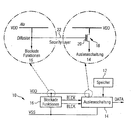
- FIG. 1 shows a schematic block diagram of a IC's, in the memory of which 12 security-relevant data are stored are.
- the integrated circuit 10 thus has a memory 12 connected to a readout circuit 14 is. From the readout circuit 14, the memory 12 read data on the designated "Data" Led out.
- the power supply of the access control circuits 16 and the readout circuit 14 is arranged such that both branches of the power supply, V DD and V SS are led first to the access control circuits 16 and then to the readout circuit 14.
- a simple disconnection of V DD or V SS in front of the access control circuits 16 automatically also de-energizes the read-out circuit 14, so that no more data can be read from the memory 12.
- V DD and V SS supplies are routed in the aluminum layer as usual.
- V DD is interrupted in front of and behind the blocking functions and the readout circuit is supplied separately by a power supply directly attached to the aluminum.
- an NMOS switch 18 is additionally connected between V DD and the read-out circuit 14 at the point at which the power supply to the read-out circuit 14 branches off from that in the aluminum layer V DD , the gate 20 of which is connected to a in a security layer or line 22 guided in the diffusion is connected to the power supply of the access control circuits 16 in the diffusion plane.
- the enable signal BLCK from the access control circuit 16 to the read-out circuit 14 is carried twice and inversely. This means that the signal is positive as a BLCK signal and negative as BLCK Signal is present.
- the readout circuit can only read out data if both signals are correct. If the power supply to the access control circuits 16 is now interrupted, at least one of these signals is "wrong" and the readout circuit is blocked. It is even independent of whether V DD or V SS is interrupted. The readout circuit 14 is blocked in any case.
- the security can be increased still further in that the inverse blocking signals belonging to each other are routed parallel to one another in the integrated circuit and preferably in the diffusion or in a security layer.
- circuit blocks with regard to the supply wiring so that the block generating the control signal in front of the circuit blocks lies that generate the secret signals. With the blockade signal then when the supply is disconnected, that too secret signal destroyed.
- control signals are parallel with their inverse counterparts guided from block to block to ensure that the evaluating block that both supply polarities at the generating block issue.
- FIG. 1 shows an arrangement in one as an exemplary embodiment Memory module in which those read from the memory 12 Data via a block function for read access be blocked.
- Blockade and readout circuit are arranged so that a disconnection of the blockage function from the supply at the same time the readout circuit is switched off and thus blocked.
- the blockage signal BLCK is parallel to its inverse counterpart led to the readout circuit, where both control signals be evaluated.
- an arrangement is drawn in an enlarged representation, in which the diffusion supply of the blocking function is led to the gate of an NMOS switch which supplies the readout circuit. If the blockage circuit is separated from V DD , the readout address is disconnected from the supply at the same time.
Landscapes
- Engineering & Computer Science (AREA)
- Computer Hardware Design (AREA)
- Computer Security & Cryptography (AREA)
- General Engineering & Computer Science (AREA)
- Microelectronics & Electronic Packaging (AREA)
- Physics & Mathematics (AREA)
- General Physics & Mathematics (AREA)
- Theoretical Computer Science (AREA)
- Semiconductor Integrated Circuits (AREA)
- Storage Device Security (AREA)
- Electronic Switches (AREA)
- Logic Circuits (AREA)
Claims (12)
- Montage d'alimentation en courant de parties (14) importantes du point de vue de la sécurité d'un circuit intégré, qui sont protégées par des circuits (16) correspondants de contrôle d'accès, caractérisé en ce que l'alimentation (VDD, VSS) en courant des parties (14) qui sont importantes du point de vue de la sécurité est effectuée de façon à ce que cette alimentation (VDD, VSS) en courant soit interrompue si l'alimentation en courant des circuits (16) de contrôle d'accès est perturbée.
- Montage suivant la revendication 1, caractérisé en ce que l'alimentation en courant des parties (14) importantes du point de vue de la sécurité est raccordée à l'alimentation en courant des circuits (16) de contrôle d'accès.
- Montage suivant la revendication 1, caractérisé en ce que l'alimentation en courant des parties (14) ayant de l'importance du point de vue de la sécurité s'effectue par un ou par plusieurs commutateurs (18) qui s'ouvrent si l'alimentation en courant des circuits (16) de contrôle d'accès est perturbée.
- Montage suivant la revendication 3, caractérisé en ce qu'un commutateur (18) NMOS est monté entre l'alimentation VDD en courant et l'alimentation en courant des parties (14) importantes du point de vue de la sécurité, commutateur dont la grille (20) est reliée par une ligne (22) passant dans la diffusion ou dans une Security Layer à l'alimentation en courant VDD des circuits (16) de contrôle d'accès.
- Circuit intégré de traitement de données importantes du point de vue de la sécurité comprenant des circuits (14) d'émission de données et des circuits (16) de contrôle d'accès, caractérisé en ce qu'une perturbation de l'alimentation en courant des circuits (16) de contrôle d'accès entraíne un blocage des circuits d'émission de données.
- Circuit intégré suivant la revendication 5, caractérisé en ce qu'il est produit par les circuits (16) de contrôle d'accès des signaux (BCLK,
BCLK ) de blocage qui sont respectivement inverses par paires et les circuits (14) d'émission de données ne fonctionnent que si respectivement deux signaux (BLCK,BLCK ) inverses de blocage indiquent une cessation du blocage. - Circuit intégré suivant la revendication 6, caractérisé en ce que les signaux (BLCK,
BLCK ) inverses de blocage se correspondant respectivement l'un à l'autre, sont envoyés en parallèle l'un à l'autre et, de préférence, en étant superposés dans le circuit intégré. - Circuit intégré suivant la revendication 6 ou 7, caractérisé en ce que les signaux (BLCK,
BLCK ) de blocage passent dans la diffusion ou dans une Security Layer. - Circuit intégré suivant la revendication 5, caractérisé en ce que l'alimentation en courant des circuits (14) d'émission de données est effectuée de façon à ce que cette alimentation en courant soit interrompue, si l'alimentation en courant des circuits (16) de contrôle d'accès est perturbée.
- Circuit intégré suivant la revendication 6, caractérisé en ce que l'alimentation en courant des circuits (14) d'émission de données est raccordée à l'alimentation en courant des circuits (16) de contrôle d'accès.
- Circuit intégré suivant la revendication 9, caractérisé en ce que l'alimentation en courant des circuits (14) d'émission de données s'effectue par un ou par plusieurs commutateurs (18) qui s'ouvrent si l'alimentation en courant des circuits (16) de contrôle d'accès est perturbée.
- Circuit intégré suivant la revendication 11, caractérisé en ce qu'un commutateur (18) NMOS est monté entre l'alimentation VDD en courant et l'alimentation en courant des circuits (14) d'émission de données, la grille (20) de ce commutateur étant reliée par une ligne (22) qui passe dans la diffusion ou dans une Security Layer à l'alimentation en courant VDD des circuits (16) de contrôle d'accès.
Applications Claiming Priority (3)
| Application Number | Priority Date | Filing Date | Title |
|---|---|---|---|
| DE19938890A DE19938890C2 (de) | 1999-08-17 | 1999-08-17 | Integrierter Schaltkreis und Schaltungsanordnung zur Stromversorgung eines integrierten Schaltkreises |
| DE19938890 | 1999-08-17 | ||
| PCT/DE2000/002792 WO2001013330A1 (fr) | 1999-08-17 | 2000-08-17 | Circuit de commutation integre et circuiterie d'alimentation en courant d'un circuit de commutation integre |
Publications (2)
| Publication Number | Publication Date |
|---|---|
| EP1222621A1 EP1222621A1 (fr) | 2002-07-17 |
| EP1222621B1 true EP1222621B1 (fr) | 2003-11-05 |
Family
ID=7918616
Family Applications (1)
| Application Number | Title | Priority Date | Filing Date |
|---|---|---|---|
| EP00962227A Expired - Lifetime EP1222621B1 (fr) | 1999-08-17 | 2000-08-17 | Circuit de commutation integre et circuiterie d'alimentation en courant d'un circuit de commutation integre |
Country Status (8)
| Country | Link |
|---|---|
| US (1) | US6633501B2 (fr) |
| EP (1) | EP1222621B1 (fr) |
| JP (1) | JP2003507798A (fr) |
| CN (1) | CN1200393C (fr) |
| AT (1) | ATE253756T1 (fr) |
| DE (2) | DE19938890C2 (fr) |
| ES (1) | ES2209980T3 (fr) |
| WO (1) | WO2001013330A1 (fr) |
Families Citing this family (9)
| Publication number | Priority date | Publication date | Assignee | Title |
|---|---|---|---|---|
| DE10111029C1 (de) * | 2001-03-07 | 2002-08-22 | Infineon Technologies Ag | Depassivierungssensor als Analysierschutz für Halbleiterbauelemente oder integrierte Schaltungen |
| US6459629B1 (en) * | 2001-05-03 | 2002-10-01 | Hrl Laboratories, Llc | Memory with a bit line block and/or a word line block for preventing reverse engineering |
| DE10218096A1 (de) * | 2002-04-23 | 2003-11-13 | Infineon Technologies Ag | Integrierte Schaltung |
| US7570533B1 (en) | 2006-12-13 | 2009-08-04 | Arrowhead Center, Inc. | Completely transportable erasable memory apparatus and method |
| CN103605936A (zh) | 2008-06-24 | 2014-02-26 | Nds有限公司 | 集成电路内的安全 |
| US8325543B2 (en) * | 2010-02-26 | 2012-12-04 | International Business Machines Corporation | Global bit select circuit interface with false write through blocking |
| US8325549B2 (en) * | 2010-02-26 | 2012-12-04 | International Business Machines Corporation | Global bit select circuit interface with simplified write bit line precharging |
| US8638595B2 (en) | 2012-04-16 | 2014-01-28 | International Business Machines Corporation | Global bit select circuit with write around capability |
| DE102017103418B4 (de) * | 2017-02-20 | 2019-01-24 | Infineon Technologies Ag | Verfahren zum Bestimmen von Informationen über eine Integrität von Signalverarbeitungskomponenten innerhalb eines Signalpfades, Signalverarbeitungsschaltung und elektronische Steuerungseinheit |
Family Cites Families (9)
| Publication number | Priority date | Publication date | Assignee | Title |
|---|---|---|---|---|
| GB2182176B (en) * | 1985-09-25 | 1989-09-20 | Ncr Co | Data security device for protecting stored data |
| EP0509567A3 (en) * | 1991-03-28 | 1993-04-07 | N.V. Philips' Gloeilampenfabrieken | Device with protection against access to secure information |
| GB2288048A (en) * | 1994-03-29 | 1995-10-04 | Winbond Electronics Corp | Intergrated circuit |
| FR2727227B1 (fr) * | 1994-11-17 | 1996-12-20 | Schlumberger Ind Sa | Dispositif de securite actif a memoire electronique |
| FR2728369B1 (fr) | 1994-12-19 | 1997-01-31 | Sgs Thomson Microelectronics | Procede et dispositif pour accroitre la securite d'un circuit integre |
| DE19610070A1 (de) * | 1996-03-14 | 1997-09-18 | Siemens Ag | Chipkarte |
| US5880523A (en) * | 1997-02-24 | 1999-03-09 | General Instrument Corporation | Anti-tamper integrated circuit |
| DE19752695A1 (de) * | 1997-11-28 | 1999-06-02 | Angewandte Digital Elektronik | Elektronisches Schaltelement zur Sperrung von elektronischen Teilen in einer Chipkarte |
| US6292898B1 (en) * | 1998-02-04 | 2001-09-18 | Spyrus, Inc. | Active erasure of electronically stored data upon tamper detection |
-
1999
- 1999-08-17 DE DE19938890A patent/DE19938890C2/de not_active Expired - Fee Related
-
2000
- 2000-08-17 JP JP2001517349A patent/JP2003507798A/ja not_active Withdrawn
- 2000-08-17 CN CNB00811708XA patent/CN1200393C/zh not_active Expired - Fee Related
- 2000-08-17 EP EP00962227A patent/EP1222621B1/fr not_active Expired - Lifetime
- 2000-08-17 ES ES00962227T patent/ES2209980T3/es not_active Expired - Lifetime
- 2000-08-17 WO PCT/DE2000/002792 patent/WO2001013330A1/fr not_active Ceased
- 2000-08-17 DE DE50004366T patent/DE50004366D1/de not_active Expired - Lifetime
- 2000-08-17 AT AT00962227T patent/ATE253756T1/de active
-
2002
- 2002-02-19 US US10/078,149 patent/US6633501B2/en not_active Expired - Lifetime
Also Published As
| Publication number | Publication date |
|---|---|
| US20020088997A1 (en) | 2002-07-11 |
| DE50004366D1 (de) | 2003-12-11 |
| ATE253756T1 (de) | 2003-11-15 |
| WO2001013330A1 (fr) | 2001-02-22 |
| EP1222621A1 (fr) | 2002-07-17 |
| CN1200393C (zh) | 2005-05-04 |
| US6633501B2 (en) | 2003-10-14 |
| DE19938890C2 (de) | 2001-08-09 |
| CN1370304A (zh) | 2002-09-18 |
| DE19938890A1 (de) | 2001-03-22 |
| ES2209980T3 (es) | 2004-07-01 |
| JP2003507798A (ja) | 2003-02-25 |
Similar Documents
| Publication | Publication Date | Title |
|---|---|---|
| EP1053518B1 (fr) | Circuit de protection pour circuit integre | |
| DE3635938C2 (fr) | ||
| DE60130154T2 (de) | Ein kartenlesegerät | |
| DE60319941T2 (de) | Gehäuse mit Einbruchschutz für elektronische Schaltungen | |
| DE3818960C2 (fr) | ||
| EP1149358B1 (fr) | Carte a puce sans contact | |
| DE102013108016A1 (de) | Sicherheitshülle | |
| EP1222621B1 (fr) | Circuit de commutation integre et circuiterie d'alimentation en courant d'un circuit de commutation integre | |
| DE10223176B3 (de) | Integrierte Schaltung mit sicherheitskritischen Schaltungskomponenten | |
| DE69528449T2 (de) | Integrierte Halbleiterschaltungsanordnung zum Schutz mehrerer Hilfsmittel in einer elektronischen Einheit | |
| DE4312905A1 (de) | Schutzeinrichtung zur Sicherung von gespeicherten Daten | |
| EP1080454B1 (fr) | Support de donnees a acces protege | |
| DE19600769A1 (de) | Sicherheitsmodul mit einteiliger Sicherheitsfolie | |
| EP0276450A1 (fr) | Circuit de protection de données pour le blocage de la transmission de signaux sur un bus | |
| DE10344647B3 (de) | Schaltungsanordnung und Verfahren zur Verarbeitung eines Dual-Rail-Signals | |
| EP1323015B1 (fr) | Module de securite | |
| DE10337567B3 (de) | Schutzstruktur für Hardware mit hochauflösenden Elastomeren | |
| DE10340289A1 (de) | Sicherungseinrichtung für Hardwarebaugruppen | |
| DE10140045B4 (de) | IC-Chip mit Schutzstruktur | |
| DE10164419A1 (de) | Verfahren und Anordnung zum Schutz von digitalen Schaltungsteilen | |
| DE10045025A1 (de) | IC-Packung mit einer Sicherheitseinrichtung | |
| EP1495542B1 (fr) | Circuit et procede pour produire un signal de sortie double voie | |
| DE10162310A1 (de) | Verfahren und Anordnung zur Übertragung von Signalen von erzeugenden Funktionseinheiten an verarbeitende Funktionseinheiten elektrischer Schaltungen | |
| DE202004008380U1 (de) | Sicherer Kartenleser | |
| EP1058178B1 (fr) | Circuit de protection |
Legal Events
| Date | Code | Title | Description |
|---|---|---|---|
| PUAI | Public reference made under article 153(3) epc to a published international application that has entered the european phase |
Free format text: ORIGINAL CODE: 0009012 |
|
| 17P | Request for examination filed |
Effective date: 20020117 |
|
| AK | Designated contracting states |
Kind code of ref document: A1 Designated state(s): AT BE CH CY DE DK ES FI FR GB GR IE IT LI LU MC NL PT SE |
|
| 17Q | First examination report despatched |
Effective date: 20021016 |
|
| GRAH | Despatch of communication of intention to grant a patent |
Free format text: ORIGINAL CODE: EPIDOS IGRA |
|
| GRAS | Grant fee paid |
Free format text: ORIGINAL CODE: EPIDOSNIGR3 |
|
| GRAA | (expected) grant |
Free format text: ORIGINAL CODE: 0009210 |
|
| AK | Designated contracting states |
Kind code of ref document: B1 Designated state(s): AT DE ES FR GB IT |
|
| REG | Reference to a national code |
Ref country code: GB Ref legal event code: FG4D Free format text: NOT ENGLISH |
|
| REF | Corresponds to: |
Ref document number: 50004366 Country of ref document: DE Date of ref document: 20031211 Kind code of ref document: P |
|
| REG | Reference to a national code |
Ref country code: IE Ref legal event code: FG4D Free format text: GERMAN |
|
| GBT | Gb: translation of ep patent filed (gb section 77(6)(a)/1977) |
Effective date: 20040120 |
|
| REG | Reference to a national code |
Ref country code: IE Ref legal event code: FD4D |
|
| REG | Reference to a national code |
Ref country code: ES Ref legal event code: FG2A Ref document number: 2209980 Country of ref document: ES Kind code of ref document: T3 |
|
| ET | Fr: translation filed | ||
| PG25 | Lapsed in a contracting state [announced via postgrant information from national office to epo] |
Ref country code: ES Free format text: LAPSE BECAUSE OF NON-PAYMENT OF DUE FEES Effective date: 20040818 |
|
| PLBE | No opposition filed within time limit |
Free format text: ORIGINAL CODE: 0009261 |
|
| STAA | Information on the status of an ep patent application or granted ep patent |
Free format text: STATUS: NO OPPOSITION FILED WITHIN TIME LIMIT |
|
| 26N | No opposition filed |
Effective date: 20040806 |
|
| PG25 | Lapsed in a contracting state [announced via postgrant information from national office to epo] |
Ref country code: IT Free format text: LAPSE BECAUSE OF NON-PAYMENT OF DUE FEES Effective date: 20050817 |
|
| REG | Reference to a national code |
Ref country code: ES Ref legal event code: FD2A Effective date: 20040818 |
|
| PGFP | Annual fee paid to national office [announced via postgrant information from national office to epo] |
Ref country code: DE Payment date: 20141023 Year of fee payment: 15 |
|
| REG | Reference to a national code |
Ref country code: FR Ref legal event code: PLFP Year of fee payment: 16 |
|
| PGFP | Annual fee paid to national office [announced via postgrant information from national office to epo] |
Ref country code: GB Payment date: 20150819 Year of fee payment: 16 |
|
| PGFP | Annual fee paid to national office [announced via postgrant information from national office to epo] |
Ref country code: AT Payment date: 20150820 Year of fee payment: 16 Ref country code: FR Payment date: 20150820 Year of fee payment: 16 |
|
| REG | Reference to a national code |
Ref country code: DE Ref legal event code: R119 Ref document number: 50004366 Country of ref document: DE |
|
| PG25 | Lapsed in a contracting state [announced via postgrant information from national office to epo] |
Ref country code: DE Free format text: LAPSE BECAUSE OF NON-PAYMENT OF DUE FEES Effective date: 20160301 |
|
| REG | Reference to a national code |
Ref country code: AT Ref legal event code: MM01 Ref document number: 253756 Country of ref document: AT Kind code of ref document: T Effective date: 20160817 |
|
| GBPC | Gb: european patent ceased through non-payment of renewal fee |
Effective date: 20160817 |
|
| REG | Reference to a national code |
Ref country code: FR Ref legal event code: ST Effective date: 20170428 |
|
| PG25 | Lapsed in a contracting state [announced via postgrant information from national office to epo] |
Ref country code: AT Free format text: LAPSE BECAUSE OF NON-PAYMENT OF DUE FEES Effective date: 20160817 |
|
| PG25 | Lapsed in a contracting state [announced via postgrant information from national office to epo] |
Ref country code: GB Free format text: LAPSE BECAUSE OF NON-PAYMENT OF DUE FEES Effective date: 20160817 Ref country code: FR Free format text: LAPSE BECAUSE OF NON-PAYMENT OF DUE FEES Effective date: 20160831 |