EP1223620A2 - Sturcture de protection contre les décharges électrostatiques - Google Patents
Sturcture de protection contre les décharges électrostatiques Download PDFInfo
- Publication number
- EP1223620A2 EP1223620A2 EP01129742A EP01129742A EP1223620A2 EP 1223620 A2 EP1223620 A2 EP 1223620A2 EP 01129742 A EP01129742 A EP 01129742A EP 01129742 A EP01129742 A EP 01129742A EP 1223620 A2 EP1223620 A2 EP 1223620A2
- Authority
- EP
- European Patent Office
- Prior art keywords
- source
- drain
- semiconductor substrate
- electrostatic discharge
- protection structure
- Prior art date
- Legal status (The legal status is an assumption and is not a legal conclusion. Google has not performed a legal analysis and makes no representation as to the accuracy of the status listed.)
- Withdrawn
Links
- 239000000758 substrate Substances 0.000 claims abstract description 41
- 239000004065 semiconductor Substances 0.000 claims abstract description 38
- 238000009792 diffusion process Methods 0.000 claims abstract description 23
- 230000015556 catabolic process Effects 0.000 claims abstract description 14
- 239000003989 dielectric material Substances 0.000 claims 2
- 230000003071 parasitic effect Effects 0.000 description 14
- 229910021420 polycrystalline silicon Inorganic materials 0.000 description 13
- 229920005591 polysilicon Polymers 0.000 description 13
- 239000002184 metal Substances 0.000 description 9
- XUIMIQQOPSSXEZ-UHFFFAOYSA-N Silicon Chemical compound [Si] XUIMIQQOPSSXEZ-UHFFFAOYSA-N 0.000 description 8
- 229910052710 silicon Inorganic materials 0.000 description 8
- 239000010703 silicon Substances 0.000 description 8
- 229910021332 silicide Inorganic materials 0.000 description 6
- FVBUAEGBCNSCDD-UHFFFAOYSA-N silicide(4-) Chemical compound [Si-4] FVBUAEGBCNSCDD-UHFFFAOYSA-N 0.000 description 6
- 238000012421 spiking Methods 0.000 description 6
- 238000000034 method Methods 0.000 description 5
- 230000009471 action Effects 0.000 description 4
- 230000004888 barrier function Effects 0.000 description 4
- 238000010438 heat treatment Methods 0.000 description 4
- 230000000694 effects Effects 0.000 description 3
- 230000005684 electric field Effects 0.000 description 3
- 239000007943 implant Substances 0.000 description 3
- 238000002513 implantation Methods 0.000 description 3
- 238000004519 manufacturing process Methods 0.000 description 3
- 230000007246 mechanism Effects 0.000 description 3
- 230000008569 process Effects 0.000 description 3
- 238000005275 alloying Methods 0.000 description 2
- 238000013459 approach Methods 0.000 description 2
- 230000015572 biosynthetic process Effects 0.000 description 2
- 238000005516 engineering process Methods 0.000 description 2
- 230000004807 localization Effects 0.000 description 2
- 239000000463 material Substances 0.000 description 2
- 238000012986 modification Methods 0.000 description 2
- 230000004048 modification Effects 0.000 description 2
- 230000003068 static effect Effects 0.000 description 2
- VYPSYNLAJGMNEJ-UHFFFAOYSA-N Silicium dioxide Chemical compound O=[Si]=O VYPSYNLAJGMNEJ-UHFFFAOYSA-N 0.000 description 1
- 239000004020 conductor Substances 0.000 description 1
- 230000005496 eutectics Effects 0.000 description 1
- 230000001939 inductive effect Effects 0.000 description 1
- 238000005468 ion implantation Methods 0.000 description 1
- 238000002955 isolation Methods 0.000 description 1
- 230000008018 melting Effects 0.000 description 1
- 238000002844 melting Methods 0.000 description 1
- 229910001092 metal group alloy Inorganic materials 0.000 description 1
- 229910044991 metal oxide Inorganic materials 0.000 description 1
- 150000004706 metal oxides Chemical class 0.000 description 1
- 230000009290 primary effect Effects 0.000 description 1
- 229910052814 silicon oxide Inorganic materials 0.000 description 1
Images

Classifications
-
- H—ELECTRICITY
- H10—SEMICONDUCTOR DEVICES; ELECTRIC SOLID-STATE DEVICES NOT OTHERWISE PROVIDED FOR
- H10D—INORGANIC ELECTRIC SEMICONDUCTOR DEVICES
- H10D89/00—Aspects of integrated devices not covered by groups H10D84/00 - H10D88/00
- H10D89/60—Integrated devices comprising arrangements for electrical or thermal protection, e.g. protection circuits against electrostatic discharge [ESD]
- H10D89/601—Integrated devices comprising arrangements for electrical or thermal protection, e.g. protection circuits against electrostatic discharge [ESD] for devices having insulated gate electrodes, e.g. for IGFETs or IGBTs
- H10D89/811—Integrated devices comprising arrangements for electrical or thermal protection, e.g. protection circuits against electrostatic discharge [ESD] for devices having insulated gate electrodes, e.g. for IGFETs or IGBTs using FETs as protective elements
- H10D89/813—Integrated devices comprising arrangements for electrical or thermal protection, e.g. protection circuits against electrostatic discharge [ESD] for devices having insulated gate electrodes, e.g. for IGFETs or IGBTs using FETs as protective elements specially adapted to provide an electrical current path other than the field-effect induced current path
- H10D89/815—Integrated devices comprising arrangements for electrical or thermal protection, e.g. protection circuits against electrostatic discharge [ESD] for devices having insulated gate electrodes, e.g. for IGFETs or IGBTs using FETs as protective elements specially adapted to provide an electrical current path other than the field-effect induced current path involving a parasitic bipolar transistor triggered by the local electrical biasing of the layer acting as base region of said parasitic bipolar transistor
Definitions
- the present invention relates to electrostatic discharge (ESD) protection structures and more particularly to ESD protection transistor structures for deep-quarter micron line geometries.
- Electrostatic discharges are high-voltage spikes of static charges which damage modern integrated circuits. ESDs are a significant failure mechanism, particularly as integrated circuit physical dimensions continue to shrink to the deep-quarter micron range.
- an ESD occurs upon contact of one or more of the terminals of an integrated circuit with a body or material that is statically charged to a high voltage. This level of static charge is readily generated by the triboelectric effect, and other mechanisms acting upon humans, equipment, or the circuits themselves. Upon contact, the integrated circuit discharges through its active devices and DC current paths. If the amount of charge is excessive however, the discharge current density can permanently damage the integrated circuit so that it is no longer functional or so that it is more prone to later-life failure. ESD damage thus is a cause of yield loss in manufacturing and also poor reliability in use.
- NMOS n-type metal oxide semiconductor
- the NMOS performance is limited because the peak heating occurs close to the surface of the transistor in the silicon which has poor thermal conductivity. Therefore, an ESD implant has to be used to make the junction deeper as well as to overdope the lightly doped region of the diffusion for improved ESD performance. Further, the thin oxide is easily damaged, especially for the ESD paths near the interface of the thin oxide and the p-substrate.
- silicide block The most conventional solution to the salicidation problem is called a "salicide block".
- Most salicidation fabrication technology processes have a “salicide block” option, which is an additional photolithographic process step to block the formation of silicide in areas close to a transistor's gate edge. Without the gate edge silicide, an ESD implantation is required make the drain junction deeper as well as to overdope the lightly doped region of the diffusion for better ESD performance. Since the ESD implantation is undesirable in the integrated circuits being protected, an ESD implant block would be required over the non-ESD circuits. Thus, this approach adds to process complexity because it requires at least two additional photolithographic process steps; i.e., the silicide block and the ESD implant block.
- the majority of the electrons reaching the collector junction are emitted from the emitter junction sidewall of the diffusion region, which results in a very small "intrinsic" base area.
- the high current is confined to a very small region of the emitter and base regions which leads to a large power density in these regions and hence higher temperatures.
- the substrate current initially needs to forward-bias a small region of the source-substrate junction to turn "on" the bipolar action.
- a larger emitter area is preferred. This will be particularly effective if the source barrier lowering occurs deeper in the junction, allowing the power dissipation to take place deeper in the device to reduce the temperature rise in the device.
- the field oxide device is a better protection element for large feature size technologies since the bipolar action takes place deeper in the silicon and the peak heating is located further away from the silicon surface.
- the FOD performance is limited and the onset of damage has been observed at low-voltage levels.
- the FOD might be again useable to provide ESD protection with a smaller layout area. This ideal has been long sought, but has also equally as long eluded those skilled in the art.
- the present invention provides an electrostatic discharge protection structure with a dielectric gate, source and drain contacts, and a semiconductor substrate.
- the semiconductor substrate is of a first conductivity type having the dielectric gate disposed partially on its surface.
- the source and drain contacts are connected to source and drain diffusion regions of a second conductivity type separated by the dielectric gate.
- Deep source and drain wells of the second conductivity type respectively disposed under the source and drain diffusion regions define a channel region of the first conductivity type.
- the channel region is doped so that the surface breakdown voltage is exceeded before the subsurface depletion region punch-through voltage between the deep source and drain wells upon an electrostatic discharge at the drain contact.
- the structure is less subject to heat damage and provides excellent ESD protection in a small layout area.
- the present invention further provides an electrostatic discharge protection structure with a dielectric gate, source and drain contacts, and a semiconductor substrate connected to a bonding pad on a dielectric layer containing a polysilicon tab and disposed over a floating well in the semiconductor substrate.
- the semiconductor substrate is of a first conductivity type having the dielectric gate disposed partially on its surface.
- the source and drain contacts are connected to source and drain diffusion regions of a second conductivity type separated by the dielectric gate. Deep source and drain wells of the second conductivity type respectively disposed under the source and drain diffusion regions define a channel region of the first conductivity type.
- the channel region is doped so that the surface breakdown voltage is exceeded before the subsurface depletion region punch-through voltage between the deep source and drain wells upon an electrostatic discharge at the drain contact.
- the structure includes a bonding pad connected to the drain contact and disposed over a dielectric layer containing a polysilicon tab.
- the dielectric layer in turn is disposed over a floating well in the semiconductor substrate.
- the surface of the bonding pad is often punched with holes through the metal layer and have microcracks in the dielectric layer. These holes and microcracks help generate high electrical fields in the damaged dielectric layer and cause metal spiking when a high-voltage ESD is applied to the bonding pad.
- the polysilicon tab and the floating well provide protection against the ESD induced metal spiking.
- the ESD protection structure 10 includes a low turn-on voltage, field oxide device (FOD) 12 having its source connected to a ground 14, its drain connected through a diode 16 to the ground 14, and its gate connected to its drain.
- FOD field oxide device
- the drain of the FOD 12 is connected to an input bonding pad 18 and a polysilicon tab 20.
- the polysilicon tab 20 is disposed over a floating n-well 22 and is capacitively coupled to the ground 14.
- the input bonding pad 18 is further connected to a first attenuation resistor 24 which is capacitively coupled by a first diode 26 to the ground 14.
- the first attenuation resistor 24 is connected to the drain and gate of a power supply discharge transistor 28 which has its source connected to a power supply (Vdd) line 30.
- the drain and gate of the power supply discharge transistor 28 is further connected to a second attenuation resistor 32 which is capacitively coupled by a second diode 34 to the ground 14.
- the second attenuation resistor 32 is then connected to the input of the integrated circuits (not shown) which is to be protected by the ESD protection structure 10.
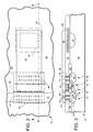
- FIG. 2 therein is shown a plan view of a portion of the ESD protection structure 10 looking down at the horizontal surface of a portion of a silicon semiconductor substrate 40.
- horizontal as used in herein is defined as a plane parallel to the conventional plane or surface of the semiconductor substrate 40, regardless of the orientation of the semiconductor substrate 40.
- vertical refers to a direction perpendicular to the horizontal as just defined. Prepositions, such as “on”, “below”, “above”, “beneath”, “lower”, “over”, and “under” are defined with respect to the conventional plane or surface being on the top surface of the semiconductor substrate 40, regardless of the orientation of the semiconductor substrate 40.
- FIG. 2 are shown the FOD 12 and the input bonding pad 18.
- the FOD 12 is shown with the source 42 connected by a plurality of source contacts 44 to the ground 14. Also shown is the drain 46 of the FOD 12 connected by a plurality of drain contacts 48 to the input bonding pad 18.
- a p-doped channel region 50 of the FOD 12 is shown under a polysilicon gate 52.
- FIG. 3 therein is shown a cross-section of FIG. 2 taken along the line 3 -- 3.
- the FOD 12 has a field oxide (FOX) 56 deposited over the p-doped channel region 50 and the polysilicon gate 52 deposited above the p-doped channel region 50.
- FOX field oxide
- Implanted into the semiconductor substrate 40 between the FOX 56 and an isolation FOX 58 are deep n-wells 60 and 62 and respective n+ diffusion regions 64 and 66.
- the n-wells 60 and 62 are referred to as being deep because they are at least twice as deep as the respective n+ diffusion regions 64 and 66.
- the deep n-wells 60 and 62 make up the emitter and collector junctions of a parasitic lateral bipolar structure and the p-doped channel region 50 the base area. Respective sidewalls of the deep n-wells 60 and 62 form large parasitic "intrinsic" emitter and collector areas 68 and 70 and the length of the p-doped channel region 50 or base area between the parasitic "intrinsic" emitter and collector areas 68 and 70 define the parasitic "intrinsic" base length.
- n-well 60 and the n+ diffusion region 64 form the source 42 and the n-well 62 and the n+ diffusion region 66 form the drain 46.
- n+ diffusion region 64 and n+ diffusion region 66 are respective source and drain contacts 44 and 48.
- the depletion region of the drain 46 is shown as subsurface depletion region 72.
- a light ion implantation is used to set the surface doping profile of the p-doped channel region 50 to be of an opposite conductivity (p-) to that of the source 42 and the drain 46 and to have the effect of reducing the breakdown voltage of the parasitic "intrinsic" collector area 70.
- the breakdown voltage is chosen to be in the subsurface region near the parasitic "intrinsic" collector area 70 to provide an ideal low-trigger voltage so that the surface breakdown under the polysilicon gate 52 and subsurface depletion region 72 punch-through can occur at the same time.
- the region where electrons are ejected when the source 42 is forward biased is shown as an electron ejection region 74.
- the region where electron-hole generation occurs due to impact ionization is designated as the hole generation region 76 and an arrow designates the direction of the hole current 78.
- the input bonding pad 18 Adjacent to the FOD 12 is shown the input bonding pad 18 disposed on a dielectric layer 80, generally two layers of silicon oxide, in which the polysilicon tab 20 is disposed.
- the dielectric layer 80 is deposited on the semiconductor substrate 40 over the floating n-well 22.
- the ESD protection structure 10 with the FOD 12 and the bonding pad 18 is provided at the input to the integrated circuits to protect against major ESDs and relieve ESD stress on the integrated circuits located after the first and second attenuation resistors 24 and 32.
- the charge at the bonding pad 18 is conducted to the drain 46 of the FOD 12.
- a high electric field intensity is established across the parastic "intrinsic" collector area 70, resulting in an impact ionization phenomenon which produces electron holes 76.
- the holes are responsible for a local electric potential established in the p-doped channel region 50 and the semiconductor substrate 40 which cause the hole current 78.
- the source 42 becomes forward biased. This forward bias then injects the electrons into the p-doped channel region 50 and the semiconductor substrate 40.
- the FOD 12 eventually enters a low-resistance (snap-back) state, and the excessive ESD current is then released.
- the onset of the parasitic bipolar action for the FOD 12 is determined by the n+ drain diffusion avalanche breakdown.
- the breakdown near the parasitic "intrinsic" collector area 70 of the drain 46 occurs at a low value and deep in the semiconductor substrate 40.
- the trigger voltage and the snap-back holding voltage of the FOD 12 will be low with the trigger voltage slightly lower than the snap-back holding voltage.
- the hole current 78 will be injected into the semiconductor substrate 40 and produce a potential which will make the parasitic "intrinsic" emitter area 68 to become forward biased so as to eject electrons from the electron ejection region 74.
- the breakdown occurs with the generation of electron-hole pairs, and the generated electrons are swept across the drain 46 towards the drain contacts 48 adding to the drain current.
- the generated holes drift towards the substrate contact (not shown) giving rise to the hole current 78, similar to the base current for a bipolar transistor.
- the power dissipation takes place in a large volume deep in the FOD 12 in the area of the subsurface depletion region 72 with a low temperature rise in the FOD 12 because the silicon in the semiconductor substrate 40 can conduct heat away.
- the subsurface depletion region 72 also lowers the source barrier (drain induced barrier lowering or DIBL) near the punch-through voltage.
- the deep n-wells 60 and 62 provide deep junctions with relatively smooth curvatures so that high-level ESDs may be handled.
- the deep n-wells prevent metal spiking from the source and drain contacts 44 and 48 from reaching the respective bottoms of the deep n-wells 60 and 62, nor can the metal spiking microdiffuse under the polysilicon gate 52. This prevents junction leakage as happened in the past with shallow junction devices.
- the bipolar turn-on time of the FOD 12 is the base transit time and can be kept short to provide highly responsive ESD protection.
- the length is controlled by both the profiling of the implantations as well as the depth control.
- the FOX 56 of the present invention is at least twice the depth of the n+ diffusion region and cannot be easily ruptured.
- the surface of the bonding pad 18 are often punched with holes through the metal layer and have microcracks in the dielectric layer 80. These holes and microcracks help generate high electrical fields in the damaged dielectric layer 80 when a high-voltage ESD is applied to the bonding pad 18. If the electrostatic charge cannot be quickly discharged to the semiconductor substrate 40 or Vdd line 30 due to the first attenuation resistor 24 and the diode 16, the dielectric layer 80 can be ruptured. When the dielectric layer 80 is ruptured, leakage paths of metal alloy can be formed from the bonding pad 18 through microcracks to the semiconductor substrate 40. To protect the bonding pad 18, the floating n-well 22, with a conductivity type opposite the semiconductor substrate 40 is placed under the input bonding pad 18 as an extra protection against the ESD induced metal spiking.
- the polysilicon tab 20 is added and acts as a buffer between the input bonding pad 18 and the floating n-well 22 and is connected to the gate of the FOD 12.
- the polysilicon tab 20 does not prevent alloying, but it increases the distance that an alloyed spike must travel before a leakage path can occur.
- the possibility of a metal spike making contact between the input bonding pad 18 and the semiconductor substrate 40 is drastically reduced.
- the resulting series capacitance from the input bonding pad 18 to the semiconductor substrate 40 makes the entire pad capacitance less than its capacitance without the polysilicon tab 20 and improves the speed of the integrated circuit.
- the ESD charge can couple to the floating n-well 22 and offload part of the ESD energy from the integrated circuits.
- the floating n-well 22 discharges the energy through the forward bias junction to the semiconductor substrate 40.
- the floating n-well 22 must discharge the coupled energy or it will have less absorbing power to handle multiple ESDs and its own junction could be stressed for too long and suffer damage.
- bipolar punch-through structures are used to discharge the positive ESD charge to the ground.
- the present invention further uses multiple contacts 44 and 48 which enlarge the contact perimeter so that the discharge current can be spread more evenly.
- Each contact can be used as part of the "balasting" to prevent current crowding and there is less metal available for alloying, hence junction spiking is minimized.
- the contacts are designed with a large contact area for reducing current density and form for avoiding nonuniform current flow.
Landscapes
- Metal-Oxide And Bipolar Metal-Oxide Semiconductor Integrated Circuits (AREA)
- Semiconductor Integrated Circuits (AREA)
- Insulated Gate Type Field-Effect Transistor (AREA)
Applications Claiming Priority (2)
| Application Number | Priority Date | Filing Date | Title |
|---|---|---|---|
| US759492 | 1991-09-13 | ||
| US09/759,492 US6417541B1 (en) | 2001-01-12 | 2001-01-12 | ESD protection network with field oxide device and bonding pad |
Publications (2)
| Publication Number | Publication Date |
|---|---|
| EP1223620A2 true EP1223620A2 (fr) | 2002-07-17 |
| EP1223620A3 EP1223620A3 (fr) | 2003-08-27 |
Family
ID=25055848
Family Applications (1)
| Application Number | Title | Priority Date | Filing Date |
|---|---|---|---|
| EP01129742A Withdrawn EP1223620A3 (fr) | 2001-01-12 | 2001-12-13 | Sturcture de protection contre les décharges électrostatiques |
Country Status (3)
| Country | Link |
|---|---|
| US (1) | US6417541B1 (fr) |
| EP (1) | EP1223620A3 (fr) |
| SG (1) | SG111039A1 (fr) |
Families Citing this family (10)
| Publication number | Priority date | Publication date | Assignee | Title |
|---|---|---|---|---|
| US6987301B1 (en) | 2003-04-09 | 2006-01-17 | Marvell International Ltd. | Electrostatic discharge protection |
| US6818955B1 (en) | 2003-04-09 | 2004-11-16 | Marvell International Ltd. | Electrostatic discharge protection |
| US7253453B2 (en) * | 2003-05-21 | 2007-08-07 | Industrial Technology Research Institute | Charge-device model electrostatic discharge protection using active device for CMOS circuits |
| US20050045952A1 (en) * | 2003-08-27 | 2005-03-03 | International Business Machines Corporation | Pfet-based esd protection strategy for improved external latch-up robustness |
| US7875933B2 (en) * | 2005-03-29 | 2011-01-25 | Infineon Technologies Ag | Lateral bipolar transistor with additional ESD implant |
| US7492016B2 (en) * | 2006-03-31 | 2009-02-17 | International Business Machines Corporation | Protection against charging damage in hybrid orientation transistors |
| CN102034823B (zh) * | 2009-09-30 | 2013-01-02 | 意法半导体研发(深圳)有限公司 | 用于spu和stog良好性能的功率晶体管的布局和焊盘布图规划 |
| CN102299096B (zh) * | 2010-06-22 | 2017-08-01 | 中国科学院微电子研究所 | 半导体器件的接触的制造方法及具有该接触的半导体器件 |
| US8634174B2 (en) | 2011-05-25 | 2014-01-21 | International Business Machines Corporation | Gate dielectric breakdown protection during ESD events |
| CN107275342B (zh) | 2017-06-12 | 2019-11-08 | 京东方科技集团股份有限公司 | 一种显示装置及其制备方法 |
Citations (2)
| Publication number | Priority date | Publication date | Assignee | Title |
|---|---|---|---|---|
| US5744841A (en) * | 1995-02-06 | 1998-04-28 | Motorola Inc. | Semiconductor device with ESD protection |
| US5910673A (en) * | 1997-12-04 | 1999-06-08 | Sharp Microelectronics Technology, Inc. | Locos MOS device for ESD protection |
Family Cites Families (10)
| Publication number | Priority date | Publication date | Assignee | Title |
|---|---|---|---|---|
| DE3586268T2 (de) * | 1984-05-03 | 1993-02-25 | Digital Equipment Corp | Eingangs-schutzanordnung fuer vlsi-schaltungsanordnungen. |
| JPS63119574A (ja) * | 1986-11-07 | 1988-05-24 | Toshiba Corp | 半導体装置の製造方法 |
| US5111262A (en) * | 1988-08-10 | 1992-05-05 | Actel Corporation | Structure for protecting thin dielectrics during processing |
| ATE164702T1 (de) * | 1993-05-04 | 1998-04-15 | Siemens Ag | Integrierte halbleiterschaltung mit einem schutzmittel |
| JP3320872B2 (ja) * | 1993-12-27 | 2002-09-03 | ローム株式会社 | Cmos集積回路装置 |
| US6025746A (en) * | 1996-12-23 | 2000-02-15 | Stmicroelectronics, Inc. | ESD protection circuits |
| JPH1154711A (ja) * | 1997-08-04 | 1999-02-26 | Nippon Precision Circuits Kk | 半導体装置の静電保護回路 |
| US6146913A (en) * | 1998-08-31 | 2000-11-14 | Lucent Technologies Inc. | Method for making enhanced performance field effect devices |
| US6285062B1 (en) * | 1999-05-12 | 2001-09-04 | Micron Technology, Inc. | Adjustable high-trigger-voltage electrostatic discharge protection device |
| US6177324B1 (en) * | 1999-10-28 | 2001-01-23 | Chartered Semiconductor Manufacturing, Ltd. | ESD protection device for STI deep submicron technology |
-
2001
- 2001-01-12 US US09/759,492 patent/US6417541B1/en not_active Expired - Fee Related
- 2001-12-12 SG SG200107763A patent/SG111039A1/en unknown
- 2001-12-13 EP EP01129742A patent/EP1223620A3/fr not_active Withdrawn
Patent Citations (2)
| Publication number | Priority date | Publication date | Assignee | Title |
|---|---|---|---|---|
| US5744841A (en) * | 1995-02-06 | 1998-04-28 | Motorola Inc. | Semiconductor device with ESD protection |
| US5910673A (en) * | 1997-12-04 | 1999-06-08 | Sharp Microelectronics Technology, Inc. | Locos MOS device for ESD protection |
Also Published As
| Publication number | Publication date |
|---|---|
| EP1223620A3 (fr) | 2003-08-27 |
| SG111039A1 (en) | 2005-05-30 |
| US20020093056A1 (en) | 2002-07-18 |
| US6417541B1 (en) | 2002-07-09 |
Similar Documents
| Publication | Publication Date | Title |
|---|---|---|
| EP0546698B1 (fr) | Structure de protection contre des décharges électrostatiques | |
| US7682918B2 (en) | ESD protection for semiconductor products | |
| US6822297B2 (en) | Additional n-type LDD/pocket implant for improving short-channel NMOS ESD robustness | |
| US7615417B2 (en) | Triggered silicon controlled rectifier for RF ESD protection | |
| US7205612B2 (en) | Fully silicided NMOS device for electrostatic discharge protection | |
| US6576959B2 (en) | Device and method of low voltage SCR protection for high voltage failsafe ESD applications | |
| US7986011B2 (en) | Electrostatic discharge protection device | |
| JP2006523965A (ja) | シリコンオンインシュレータ技術を対象とする静電放電(esd)保護用低電圧シリコン制御整流器(scr) | |
| US6764892B2 (en) | Device and method of low voltage SCR protection for high voltage failsafe ESD applications | |
| US6452236B1 (en) | Channel implant for improving NMOS ESD robustness | |
| US6767810B2 (en) | Method to increase substrate potential in MOS transistors used in ESD protection circuits | |
| US20090268357A1 (en) | Hybrid ESD Clamp | |
| US6310380B1 (en) | Electrostatic discharge protection transistor structure with a trench extending through the source or drain silicide layers | |
| US6417541B1 (en) | ESD protection network with field oxide device and bonding pad | |
| US6855609B2 (en) | Method of manufacturing ESD protection structure | |
| US6724050B2 (en) | ESD improvement by a vertical bipolar transistor with low breakdown voltage and high beta |
Legal Events
| Date | Code | Title | Description |
|---|---|---|---|
| PUAI | Public reference made under article 153(3) epc to a published international application that has entered the european phase |
Free format text: ORIGINAL CODE: 0009012 |
|
| AK | Designated contracting states |
Kind code of ref document: A2 Designated state(s): AT BE CH CY DE DK ES FI FR GB GR IE IT LI LU MC NL PT SE TR |
|
| AX | Request for extension of the european patent |
Free format text: AL;LT;LV;MK;RO;SI |
|
| PUAL | Search report despatched |
Free format text: ORIGINAL CODE: 0009013 |
|
| AK | Designated contracting states |
Designated state(s): AT BE CH CY DE DK ES FI FR GB GR IE IT LI LU MC NL PT SE TR |
|
| AX | Request for extension of the european patent |
Extension state: AL LT LV MK RO SI |
|
| RIC1 | Information provided on ipc code assigned before grant |
Ipc: 7H 01L 29/78 B Ipc: 7H 01L 27/02 A |
|
| 17P | Request for examination filed |
Effective date: 20040225 |
|
| AKX | Designation fees paid |
Designated state(s): AT BE CH CY DE DK ES FI FR GB GR IE IT LI LU MC NL PT SE TR |
|
| 17Q | First examination report despatched |
Effective date: 20050413 |
|
| 17Q | First examination report despatched |
Effective date: 20050413 |
|
| RIN1 | Information on inventor provided before grant (corrected) |
Inventor name: LO, KENG FOO Inventor name: DAI, JUN |
|
| STAA | Information on the status of an ep patent application or granted ep patent |
Free format text: STATUS: THE APPLICATION IS DEEMED TO BE WITHDRAWN |
|
| 18D | Application deemed to be withdrawn |
Effective date: 20120508 |