EP1225257A2 - Monocristal de SiC, procédé pour sa préparation, dispositif semiconducteur à SiC et matériau composite contenant le SiC - Google Patents
Monocristal de SiC, procédé pour sa préparation, dispositif semiconducteur à SiC et matériau composite contenant le SiC Download PDFInfo
- Publication number
- EP1225257A2 EP1225257A2 EP02250383A EP02250383A EP1225257A2 EP 1225257 A2 EP1225257 A2 EP 1225257A2 EP 02250383 A EP02250383 A EP 02250383A EP 02250383 A EP02250383 A EP 02250383A EP 1225257 A2 EP1225257 A2 EP 1225257A2
- Authority
- EP
- European Patent Office
- Prior art keywords
- sic
- single crystal
- substrate
- crystal sic
- temperature
- Prior art date
- Legal status (The legal status is an assumption and is not a legal conclusion. Google has not performed a legal analysis and makes no representation as to the accuracy of the status listed.)
- Withdrawn
Links
Images


Classifications
-
- C—CHEMISTRY; METALLURGY
- C30—CRYSTAL GROWTH
- C30B—SINGLE-CRYSTAL GROWTH; UNIDIRECTIONAL SOLIDIFICATION OF EUTECTIC MATERIAL OR UNIDIRECTIONAL DEMIXING OF EUTECTOID MATERIAL; REFINING BY ZONE-MELTING OF MATERIAL; PRODUCTION OF A HOMOGENEOUS POLYCRYSTALLINE MATERIAL WITH DEFINED STRUCTURE; SINGLE CRYSTALS OR HOMOGENEOUS POLYCRYSTALLINE MATERIAL WITH DEFINED STRUCTURE; AFTER-TREATMENT OF SINGLE CRYSTALS OR A HOMOGENEOUS POLYCRYSTALLINE MATERIAL WITH DEFINED STRUCTURE; APPARATUS THEREFOR
- C30B19/00—Liquid-phase epitaxial-layer growth
-
- H—ELECTRICITY
- H10—SEMICONDUCTOR DEVICES; ELECTRIC SOLID-STATE DEVICES NOT OTHERWISE PROVIDED FOR
- H10P—GENERIC PROCESSES OR APPARATUS FOR THE MANUFACTURE OR TREATMENT OF DEVICES COVERED BY CLASS H10
- H10P14/00—Formation of materials, e.g. in the shape of layers or pillars
- H10P14/20—Formation of materials, e.g. in the shape of layers or pillars of semiconductor materials
-
- C—CHEMISTRY; METALLURGY
- C30—CRYSTAL GROWTH
- C30B—SINGLE-CRYSTAL GROWTH; UNIDIRECTIONAL SOLIDIFICATION OF EUTECTIC MATERIAL OR UNIDIRECTIONAL DEMIXING OF EUTECTOID MATERIAL; REFINING BY ZONE-MELTING OF MATERIAL; PRODUCTION OF A HOMOGENEOUS POLYCRYSTALLINE MATERIAL WITH DEFINED STRUCTURE; SINGLE CRYSTALS OR HOMOGENEOUS POLYCRYSTALLINE MATERIAL WITH DEFINED STRUCTURE; AFTER-TREATMENT OF SINGLE CRYSTALS OR A HOMOGENEOUS POLYCRYSTALLINE MATERIAL WITH DEFINED STRUCTURE; APPARATUS THEREFOR
- C30B25/00—Single-crystal growth by chemical reaction of reactive gases, e.g. chemical vapour-deposition growth
-
- C—CHEMISTRY; METALLURGY
- C30—CRYSTAL GROWTH
- C30B—SINGLE-CRYSTAL GROWTH; UNIDIRECTIONAL SOLIDIFICATION OF EUTECTIC MATERIAL OR UNIDIRECTIONAL DEMIXING OF EUTECTOID MATERIAL; REFINING BY ZONE-MELTING OF MATERIAL; PRODUCTION OF A HOMOGENEOUS POLYCRYSTALLINE MATERIAL WITH DEFINED STRUCTURE; SINGLE CRYSTALS OR HOMOGENEOUS POLYCRYSTALLINE MATERIAL WITH DEFINED STRUCTURE; AFTER-TREATMENT OF SINGLE CRYSTALS OR A HOMOGENEOUS POLYCRYSTALLINE MATERIAL WITH DEFINED STRUCTURE; APPARATUS THEREFOR
- C30B29/00—Single crystals or homogeneous polycrystalline material with defined structure characterised by the material or by their shape
- C30B29/10—Inorganic compounds or compositions
- C30B29/36—Carbides
Definitions
- This invention broadly relates to a single crystal SiC (silicon carbide) used as a substrate material of a semiconductor device and a method of producing the same as well as a SiC semiconductor device and a SiC composite material, which are capable of reducing planar defect density of SiC.
- SiC silicon carbide
- SiC is generally a semiconductor material with a wide band gap, an excellent chemical stability, and environment resistance.
- SiC can be used under a severe condition, such as a high voltage, a high temperature, or exposure to radiation, to which a conventional semiconductor material, typically Si (silicon), is difficult to apply.
- SiC as a source material is sublimated in a crucible at a temperature within a range between 2000 and 2500°C to thereby generate a sublimation gas.
- a seed crystal formed of a SiC single crystal is placed.
- the seed crystal is retained at a temperature 50-200°C lower than that of the material.
- a new SiC single crystal is grown on the seed crystal.
- the above-mentioned method is disclosed in Japanese Examined Patent Publication No. JP 7-88274 B, and Japanese Examined Patent Publication No. JP 7-91153 B.
- a crucible containing carbon as its component element is heated to a temperature within a range of 1650-1800°C, and Si is melted in the crucible into a Si melt. Within the Si melt, SiC is generated by reaction between Si and carbon as the component element of the crucible. Then, a SiC seed crystal is contacted with the surface of the melt to thereby grow SiC. Thus, a single crystal SiC is produced.
- this method is disclosed in Japanese Unexamined Patent Publication No. JP 7-172998 A.
- SiC is used as a target material to thereby deposite a SiC film on a substrate.
- a single crystal Si or a single crystal SiC is employed as the substrate and a substrate temperature is set to 1200°C or higher to thereby produce the single crystal SiC.
- a raw material gas of Si and a raw material gas of carbon are supplied onto a Si substrate and are thermally reacted with each other in an atmosphere kept at normal pressure or reduced pressure so that SiC is deposited on a surface of the Si substrate.
- ALE atomic layer epitaxy
- a Si source and a carbon source are alternately adsorbed on the substrate surface so that SiC is epitaxially-grown, reflecting the crystallinity of the substrate.
- the substrate surface may be partially or entirely etched by an impurity gas, such as H 2 O and O 2 , existing in a reaction chamber before formation of SiC or at the same time with formation of SiC.
- an impurity gas such as H 2 O and O 2
- the partial pressure of the impurity gas, such as H 2 O and O 2 in the reaction chamber is low, an oxide having a stoichiometric composition is not formed on the substrate surface but a suboxide will be formed.
- the suboxide such as SiO is low in vapor pressure and high in volatility, and is therefore detached from the substrate surface as soon as it is formed.
- the substrate surface is etched.
- chloride is volatilized from the substrate surface, thereby causing an etching phenomenon to occur, like in case of oxygen.
- etch pit As a result of etching, a hole-like defect called an etch pit is inevitably formed on the substrate surface.
- another defect called a dome-like protrusion is formed on the substrate surface as a result of reaction between an etched substrate component and the raw material gas.
- a single crystal SiC layer partially or entirely reflecting or copying surface orientation of the substrate is not formed but a polycrystal SiC layer will be formed.
- SiC grown on the polycrystal SiC layer by vapor phase reaction has planar defects with high density and is therefore difficult to be used as a semiconductor device.
- the aforementioned planar defects include a stacking fault, an antiphase domain boundary, and a twin boundary.
- a thin single crystal SiC layer is preliminarily formed before depositing a thick SiC so as to suppress the above-mentioned etching of the substrate surface.
- the surface of the Si substrate is heat-treated in a hydrocarbon atmosphere to form an extremely thin SiC layer having a thickness of about 10 nm. This method is referred to as surface carbonization.
- the effect of suppressing the etching of the substrate surface is varied in dependency upon the partial pressure of the impurity gas such as H 2 O, O 2 , and chloride in the reaction chamber.
- the single crystal SiC low in defect density and usable as the semiconductor device could be not produced stably and industrially.
- Japanese Examined Patent Publication No. JP 8-15143 B proposes a method of forming the SiC layer by reaction between hydrocarbon and the Si substrate in a high vacuum atmosphere with remarkably low impurity concentration.
- a method of forming the SiC layer in the high vacuum atmosphere requires a long time to obtain the high vacuum atmosphere, thus being not always suitable as a production method of the industrial level.
- Japanese Unexamined Patent Publication No. JP 1-162326 A proposes formation of the SiC layer by reaction between C 2 H 2 and Si at the substrate temperature of 800°C ⁇ 1000°C. Such a low substrate temperature reduces the formation of the etch pits and trapping of the impurities.
- a grown film has a twin crystal or a polycrystal structure and the single crystal can not be grown. In order to grow the single crystal, the growth rate must be lowered. Therefore, a long production time is inevitably required to produce a thick SiC single crystal usable for the semiconductor device. Accordingly, this method is not practical also.
- a method of producing single crystal SiC on a substrate having a surface comprises a first step of forming a thin single crystal SiC layer on the surface of the substrate by heating the substrate under existence of a raw material containing C or C and Si and a second step of depositing SiC on the single crystal SiC layer by the vapor phase growth method or the liquid phase growth method.
- the vapor phase growth method includes, for example, CVD and sputtering. By the use of these methods, vapor phase epitaxy can be carried out.
- the raw material is supplied in the vicinity of the surface of the substrate.
- the raw material in the vicinity of the surface of the substrate is given a partial pressure higher at least by a predetermined rate than that of an impurity.
- the impurity is prevented from reaching the surface of the substrate, so that the surface of the substrate is prevented from being etched by the impurity.
- heating the substrate in the first step of forming the single crystal SiC layer comprises a temperature elevating step.
- the partial pressure of the raw material is adjusted to a level not lower than 100 times that of the impurity.
- the temperature of the substrate is elevated from a first temperature Te at which etching of the surface of the substrate by the impurity is started to a second temperature not lower than a temperature at which the single crystal SiC layer is formed.
- a temperature elevating rate and a temperature elevating time is selected within a range such that the density and the size of a defect, such as etch pits or dome-like protrusions, formed on the surface of the single crystal SiC layer are not so increased as to cause a planar defect on SiC which is deposited on the single crystal SiC layer by the vapor phase growth method or the liquid phase growth method.
- a defect such as etch pits or dome-like protrusions
- the material used in the first step and containing C is at least one selected from the group consisting of C n H 2n (2 ⁇ n ⁇ 3), C n H 2n+2 (1 ⁇ n ⁇ 3), C n H 2n-2 (1 ⁇ n ⁇ 3), CCl 4 , CHF 3 , and CF 4 .
- the material containing Si may be used in the first step in addition to the material containing C.
- the material containing Si is at least one selected from the group consisting of SiH 2 Cl 2 , SiH 4 , SiCl 4 , SiHCl 3 , Si 2 H 6 , and Si 2 Cl 6 .
- the material used in the first step and containing C is at least one selected from the group consisting of Si(CH 3 ) 4 , SiH 2 (CH 3 ) 2 , SiH(CH 3 ) 3 , Si 2 (CH 3 ) 6 , (CH 3 ) 3 SiCl, and (CH 3 ) 2 SiCl 2 .
- single crystal SiC is obtained by a method according to any one of the first through the fifth aspects of this invention.
- the density of defects, such as etch pits and dome-like protrusions, on a topmost surface falls within a range not higher than 10 2 /cm -2 .
- single crystal SiC is obtained by a method according to any one of the first through the fifth aspects of this invention.
- the density of planar defects on a topmost surface falls within a range not higher than 10 3 /cm -2 .
- single crystal SiC is obtained by a method according to any one of the first through the fifth aspects of this invention. Furthermore, another SiC is deposited on the single crystal SiC by the vapor phase growth method or the liquid phase growth method.
- a semiconductor device comprises SiC having a predetermined concentration of dopant and obtained by adding the dopant by ion implantation into the single crystal SiC produced by the method according to any one of the first through the fifth aspects of this invention.
- a semiconductor device comprises SiC having a predetermined concentration of dopant and obtained by adding the dopant into SiC during the second step of depositing SiC.
- a SiC composite material comprises a single crystal SiC produced by a method according to any one of the first through the fifth aspects of this invention and diamond or GaN formed on the single crystal SiC.
- SiC silicon carbide
- a substrate 101 is heated under existence of a raw material M containing C.
- the raw material may contain Si in addition to C as desired.
- a thin single crystal SiC layer 101 a is formed on the surface of the substrate 101 (hereinafter, this step may be referred to as a single crystal SiC layer formation step).
- a thick SiC layer 101b is deposited on the single crystal SiC layer 101a by the use of the vapor phase growth method or the liquid phase growth method (hereinafter, this step may be referred to as a SiC deposition step).
- the raw material M is supplied in the vicinity of the surface of the substrate 101.
- the raw material in the vicinity of the substrate surface is given a partial pressure not lower at a predetermined rate than that of an impurity.
- the impurity is prevented from reaching the substrate surface so that the substrate surface is prevented from being etched by the impurity.
- heating in the single crystal SiC layer formation step comprises a temperature elevating step.
- the temperature elevating step the partial pressure of the raw material is adjusted to a level not lower than 100 times that of the impurity.
- the temperature of the substrate is elevated from an etching start temperature Te at which etching of the substrate surface by the impurity is started to a temperature not lower than a SiC forming temperature at which the single crystal SiC layer is formed.
- At least one of a temperature elevating rate and a temperature elevating time is selected within a range such that the density and the size of the defect, such as the etch pits or the dome-like protrusions, formed on the surface of the single crystal SiC layer on the substrate surface are not increased to a level causing a planar defect on SiC which will be deposited on the single crystal SiC layer by the vapor phase growth method or the liquid phase growth method.
- Such defect is formed on the single crystal SiC layer because the surface of the substrate is etched by the impurity.
- the defect such as the etch pits or the dome-like protrusions, formed by the etching of the substrate with the impurity occurs within a temperature range not lower than Te, and is increased with time of exposure to the impurity at the temperature not lower than Te.
- the time of exposure to the impurity is reduced to a predetermined time period or less so that the density and the size of the defect, such as the etch pits and the dome-like protrusions, can be restricted to a predetermined level or less.
- the substrate use can be made of Si, SiC, titanium carbide, sapphire, diamond, or the like.
- the temperature at which the single crystal SiC layer is formed falls within the range between about 1000 and 1100°C in case where a Si substrate is used as the substrate.
- the single crystal SiC layer with high-quality having a film thickness of about 10 nm can relatively easily be formed (for example, see C. J. Mogab et al. Journal of Applied Physics Vol. 45 (1974) P1075-).
- the single crystal SiC layer with the high quality having the film thickness of about 10 nm is formed by reaction between raw material gases of Si source and carbon source at a temperature of about 800°C-1100°C.
- the single crystal SiC layer with high quality can be formed by elevating the substrate temperature preferably to 1100°C or higher.
- the etching start temperature Te of the substrate is measured in the following manner. As illustrated in Fig. 2, a substrate 101 is arranged in a case 100 and is heated by the use of a heating apparatus 102. In this event, the substrate temperature is elevated without supplying the raw material containing C or Si into the case 100. Consequently, the impurity alone exists in the case 100.
- the etching start temperature Te is a temperature at which molecules or atoms derived from the composition of the substrate start to be detected.
- the etching start temperature Te corresponds to a temperature at which molecules or atoms derived from Si start to be detected.
- the etching start temperature Te corresponds to a temperature at which molecules or atoms derived from Al start to be detected.
- Fig. 3 shows a relationship between the temperature elevating rate and the density of the etch pits and the dome-like protrusions formed on the surface of the SiC layer.
- the Si substrate was heated up to 1100°C in a C 2 H 2 atmosphere by changing the temperature elevating rate.
- the partial pressure of the impurity is equal to 6 ⁇ 10 -3 Torr.
- the number (density) of the etch pits or the dome-like protrusions was observed by the use of a SEM (Scanning Electron Microscope). Specifically, the etch pits and the dome-like protrusions having a diagonal length of 20 nm or more were counted.
- the temperature elevating rate is equal to or higher than 150°C/minute, the density of the etch pits and the dome-like protrusions formed on the surface of the SiC layer is remarkably reduced so that the single crystal SiC layer with high-quality is obtained.
- Fig. 4 shows a relationship between the temperature elevating rate and the size of the etch pits formed on the surface of the SiC layer.
- the Si substrate was heated up to 1100°C in a C 2 H 2 atmosphere by changing the temperature elevating rate.
- the temperature elevating rate is equal to or higher than 150°C/minute, the size of the etch pits formed on the surface of the SiC layer is remarkably reduced so that the SiC layer with high-quality is formed. From the above, it is understood that the temperature elevating rate of 150°C/minute or more is desirable.
- the supply quantity of the raw material will be determined as follows. Specifically, according to the kinetic molecular theory, the collision rate of raw material molecules, namely, the number of molecules colliding with other molecules per unit time, is proportional to the square of the molecular density in the reaction chamber. Taking this into consideration, the partial pressure of the raw material is increased to raise the collision rate with the impurity, thereby further reducing the frequency at which the impurity reaches the substrate. Thus, the effect of this invention becomes more remarkable.
- the partial pressure of the raw material is practically set to at least 100 times that of the partial pressure of the impurity. Consequently, the collision rate becomes equal to 1/10000. This remarkably reduces the frequency at which the impurity reaches the substrate.
- the substrate is heated at the rate of 150°C/minute or more, and the partial pressure of the raw material is set to at least 100 times that of the impurity.
- the high-quality SiC layer which is remarkably low in density of etch pits and in density of the dome-like protrusions.
- the density of the defect, such as the etch pits or the dome-like protrusions, formed on the surface of the SiC layer produced according to this invention is substantially equal to 10 2 /cm 2 or lower.
- the carbon source is at least one selected from the group consisting of C n H 2n (2 ⁇ n ⁇ 3), C n H 2n+2 (1 ⁇ n ⁇ 3), C n H 2n-2 (1 ⁇ n ⁇ 3), CCl 4 , CHF 3 , and CF 4 .
- the Si source is at least one selected from the group consisting of SiH 2 Cl 2 , SiH 4 , SiCl 4 , SiHCl 3 , Si 2 H 6 , and Si 2 Cl 6 .
- the raw material gas may be at least one selected from the group consisting of Si(CH 3 ) 4 , SiH 2 (CH 3 ) 2 , SiH(CH 3 ) 3 , Si 2 (CH 3 ) 6 , (CH 3 ) 3 SiCl, and (CH 3 ) 2 SiCl 2 .
- the SiC layer can be formed only by supplying the raw material gas of the carbon.
- SiC is deposited on the single crystal SiC layer low in density of the defect by the vapor phase growth method or the liquid phase growth method.
- Such SiC is formed as a high-quality crystal because the surface structure and the crystallinity of the single crystal SiC layer low in density of the defect are reflected.
- At least two kinds of gases serving as the Si source and the carbon source or at least one raw material gas containing both Si and carbon are/is decomposed by heat or plasma to be reacted in the vapor phase or on the substrate surface, thus forming SiC on the substrate surface.
- the raw material gas used herein may be the same gas as that used in the above-mentioned formation of the SiC layer.
- Si is melted in a carbon crucible heated to 1500°C into a Si melt. Then, the surface of the single crystal SiC layer (a seed crystal) according to this invention is contacted with the surface of the melt. As a consequence, SiC is grown on the seed crystal by the melted Si and floating carbon in the melted Si.
- a SiC mass (ingot or a structural body) is formed on the single crystal SiC layer by the vapor phase growth method or the liquid phase growth method.
- the SiC mass has a high quality because the surface structure and the crystallinity of the single crystal SiC layer low in density of the defect is reflected.
- An SiC mass obtained in the conventional method has an aperture of about 3 inch at most.
- the SiC mass having an aperture of 4 inch to 6 inch or more can be formed by using the above-mentioned production method (namely, the vapor phase growth method or the liquid phase growth method) according to this invention.
- the SiC mass produced by the aforementioned method can be used as a substrate in a semiconductor device according to this invention.
- the semiconductor device is a power device, such as a shottky-barrier diode, or a light-emitting device, such as a blue light emitting diode.
- the semiconductor device according to this invention includes a composite material obtained by forming GaN or diamond on SiC.
- the substrate may be heated by a cold wall method for heating only the substrate and, alternatively, can be heated by a hot wall method for entirely heating the inside of the chamber.
- a cold wall method for heating only the substrate and, alternatively, can be heated by a hot wall method for entirely heating the inside of the chamber.
- the cold wall method only the substrate is rapidly heated before the inside of the chamber is sufficiently heated.
- the single crystal SiC layer can be formed before the impurity attached to a chamber wall is volatilized to float in the chamber.
- the raw material for forming the single crystal SiC layer is supplied from the beginning of the single crystal SiC layer formation step. Specifically, from the beginning (normally, the room temperature) of the single crystal SiC layer formation step, the raw material gas is supplied at a flow rate sufficient to achieve a predetermined partial pressure or more. In this event, the substrate surface is covered with the raw material gas. It is therefore possible to further prevent the impurity from reaching the substrate during heating.
- the substrate is heated at a predetermined temperature elevating rate or more from the etching start temperature Te to a SiC forming temperature at which SiC (silicon carbide) is formed on the substrate surface. It is desirable that the temperature elevating rate is also high from the beginning (normally, the room temperature) of the single crystal SiC formation step until the etching start temperature Te is reached. In other words, the substrate is preferably heated at the predetermined temperature elevating rate or higher from the beginning of the SiC layer formation step until such the SiC forming temperature is reached.
- a cold wall type CVD apparatus was employed.
- a single crystal Si substrate with a ⁇ 001 ⁇ plane was heated in a mixed atmosphere of C 2 H 2 and H 2 to deposit the SiC layer on the substrate.
- the etching start temperature Te of the Si substrate was measured.
- the measurement of Te was carried out by the use of the quadrupole mass spectrometer, as illustrated in Fig. 2.
- the etching start temperature Te of the Si substrate was equal to 800°C.
- the partial pressure of the impurity fell within the range between 1 ⁇ 10 -5 Torr and 5 ⁇ 10 -5 Torr in a temperature range between 800°C and 1100°C. Accordingly, in order to achieve the effect of this invention, the supply quantity of the raw material gas and the C 2 H 2 partial pressure during heating the substrate were selected as follows: 20 sccm as the C 2 H 2 flow rate, 100 sccm as the H 2 flow rate, and 6 ⁇ 10 -3 Torr as the C 2 H 2 partial pressure.
- the single crystal Si substrate having a ⁇ 001 ⁇ plane was placed in the cold wall type CVD apparatus and heated via a susceptor arranged on a carbon heater.
- the heating was carried out at a constant rate of 150°C/minute starting from the room temperature.
- the substrate was heated until the temperature of the substrate surface reached 1350°C.
- C 2 H 2 as the raw material gas and H 2 as a carrier gas were supplied onto the substrate surface from the initial stage at the room temperature.
- the flow rate and the partial pressure were 20 sccm as the C 2 H 2 flow rate, 100 sccm as the H 2 flow rate, and 6 ⁇ 10 -3 Torr as the C 2 H 2 partial pressure, as described above.
- the substrate was retained for 5 minutes in the above-mentioned mixed atmosphere of C 2 H 2 and H 2 to thereby form the single crystal SiC layer to a thickness of about 10 nm.
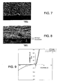
- Fig. 5 shows a SEM image of the surface of the single crystal SiC layer formed on the Si substrate surface.
- the growth of SiC was carried out as follows. After the single crystal SiC layer was formed in the above-mentioned manner, C 2 H 2 was intermittently supplied at an interval of one second while H 2 and SiH 2 Cl 2 were continuously supplied at a temperature of 1350°C. In this event, the H 2 flow rate was 100 sccm, the SiH 2 Cl 2 flow rate was 50 sccm, and the C 2 H 2 flow rate was 15 sccm.
- the pressure during growth was adjusted by a pressure-adjusting valve placed between a reaction chamber and a pump. Specifically, the pressure was set to 0.1 Torr in the mixed atmosphere of C 2 H 2 and H 2 .
- the growth was carried out under the above-mentioned growth condition for 8 hours to thereby grow 3C-SiC having a thickness of 100 ⁇ m on the single crystal SiC layer formed on the Si substrate. Then, the planar defect on the surface of SiC was observed by the use of the Nomarski microscope. As a result, the planar defect density observed on the SiC surface formed in this example was 9 ⁇ 10 2 /cm 2 .
- the electron mobility in SiC measured by the hole effect was 400 cm 2 /V/s at the room temperature.
- X-ray rocking curve measurement was carried out in order to judge the crystallinity of SiC.
- the measurement was performed for a cubic SiC (200) peak.
- a full width at half maximum of the rocking curve for the cubic SiC (200) peak of SiC grown in the above-mentioned manner was 0.05 degree.
- SiC was grown in the same manner as the first example except that the temperature elevating rate at which the substrate is heated was set to 50°C/minute, 100°C/minute, 150°C/minute, 200°C/minute, and 250°C/minute to form the single crystal SiC layers at the respective rates.
- Fig. 6 shows variation of the full width at half maximum of the rocking curve of 3C-SiC(200) peak obtained by the X-ray diffraction measurement with respect to the substrate-heating rate.
- the full width at half maximum of the rocking curve was rapidly reduced when the heating rate reached 150°C/minute or higher.
- the single crystal SiC layer was formed and SiC was grown in the same manner as the first example except that the temperature elevating rate upon heating the substrate was set to 10°C/minute.
- Fig. 7 shows a SEM image in the vicinity of the surface of the single crystal SiC layer formed on the surface of the Si substrate by the use of the method according to the first comparative example. From the figure, it is seen that the dome-like protrusions having an indefinite shape were formed at a high density on the surface of the single crystal SiC layer. Specifically, the density of the dome-like protrusions was 10 3 cm -2 on the surface of the single crystal SiC layer.
- planar defect of the SiC surface was observed by the use of the Nomarski microscope. As a result, the planar defect density observed on the SiC surface formed by the conventional method was 5 ⁇ 10 3 /cm 2 .
- the electron mobility in SiC at the room temperature was measured by the use of the hole effect. As a result, the electron mobility was 10 cm 2 /V/s.
- the crystallinity of SiC was evaluated by the X-ray rocking curve measurement. The measurement was carried out for a 3C-SiC (200) peak. As a result, the full width at half maximum of the rocking curve for 3C-SiC (200) peak grown by this method was 1.0 degree.
- the single crystal SiC layer was formed and SiC was grown in the same manner as the first example except that the temperature elevating rate upon heating the substrate was set to 3°C/minute.
- Fig. 8 shows a SEM image in the vicinity of the surface of the single crystal SiC layer formed on the surface of the Si substrate in the second comparative example.
- the etch pits exist at the interface between the single crystal SiC layer and the Si substrate. Further, the surface of the SiC layer was extremely rough. In this case, the film thickness of the SiC layer was 0.5 ⁇ m.
- the X-ray rocking curve measurement was carried out in order to judge the crystallinity of SiC.
- the measurement was performed for a 3C-SiC (200) peak.
- no peak corresponding to the 3C-SiC (200) peak could be detected from SiC grown in this method.
- SiC grown by the method of the second comparative example had a polycrystal structure.
- a schottky-barrier diode was produced by using SiC obtained according to this invention.
- the production method will hereinafter be explained.
- SiC was grown on the single crystal SiC layer formed on the Si substrate while N 2 is added.
- the growth of SiC was carried out by intermittently supplying C 2 H 2 while H 2 , SiH 2 Cl 2 and N 2 are continuously supplied.
- H 2 flow rate was100 sccm
- SiH 2 Cl 2 flow rate was 50 sccm
- N 2 flow rate was 100 sccm
- C 2 H 2 flow rate was 15 sccm.
- the pressure during growth was set to 0.1 Torr in the mixed atmosphere of C 2 H 2 and H 2 .
- the growth was carried out for 8 hours to thereby grow 3C-SiC having a thickness of 100 ⁇ m.
- atomic concentration of N in SiC was 10 20 cm -3 .
- SiC with no impurity added thereto, was formed on the above-mentioned SiC by the use of homo-epitaxial growth.
- the growth of SiC was performed at 1350°C by intermittently supplying C 2 H 2 at an interval of one second while H 2 and SiH 2 Cl 2 were continuously supplied. In this event, H 2 flow rate was 100 sccm, SiH 2 Cl 2 flow rate was 50 sccm, and C 2 H 2 flow rate was 15 sccm.
- the pressure during growth was set to 0.1 Torr in the mixed atmosphere of C 2 H 2 and H 2 .
- the growth was carried out for 1 hour to thereby grow a 3C-SiC homo-epitaxial layer having a thickness of 12.5 ⁇ m.
- the carrier density in SiC was 8 ⁇ 10 14 cm -3 .
- SiC having the homo-epitaxial layer and formed on the Si substrate was dipped in a mixed solution of nitric acid and hydrofluoric acid so that the Si substrate was dissolved and removed. It is noted here that the SiC surface was not polished. Moreover, electrodes were formed on both surfaces of SiC with the homo-epitaxail layer. A Pt electrode was formed on the homo-epitaxial layer. A Ni electrode was formed on the SiC surface. Herein, each of the electrodes had an area of 50 ⁇ m ⁇ .
- Fig. 9 shows electrical characteristics of a junction of a schottky-barrier diode according to the third example.
- a dotted line in the figure indicates the electrical characteristic related to the schottky-barrier diode using SiC grown after forming the SiC layer at the heating rate of 20°C/minute.
- a reverse leakage current was remarkably reduced in the schottky-barrier diode by setting the heating rate of the substrate to 150°C/minute according to this invention.
- the reduction of the leakage current shows that the high heating rate results in reduction of the defect density in the SiC layer and in SiC as well as flatness of the SiC surface.
- diamond or GaN was formed on the SiC obtained in the first or the second example to thereby obtain a composite material.
- the diamond can be formed on the SiC via the following steps. After SiC formed in the aforementioned examples was heated in the vacuum reaction chamber up to 500°C. Thereafter, the raw material gas was introduced into the reaction chamber. Commercial propane was used as the raw material gas of the diamond. After SiC was heated up to 500°C, high frequency wave (200W) of 13.56 MHz was applied between SiC and planar electrodes faced to SiC to thereby form plasma. Carbon was decomposed by the plasma and deposited on SiC to be placed at a proper crystal position. In this manner, formation of diamond on SiC was realized. The diamond thus formed was a cubic crystal like SiC serving as a base substrate of growth with the surface having a (001) plane.
- GaN could be formed on SiC via the following steps. After SiC formed in the above-mentioned examples was heated up to 1000°C in the vacuum reaction chamber, the raw material gas was supplied in the reaction chamber to thereby form GaN. In this event, Ga(CH 3 ) 3 was used as the raw material of Ga and supplied by bubbling. The flow rate of Ga(CH 3 ) 3 was set to 2.5 ⁇ 10 -6 mol/minute. Moreover, NH 3 was used as the raw material of nitrogen. The flow rate of NH 3 was set to 5 liter/minute. H 2 gas was used as the carrier gas. The flow rate of H 2 was se to 5 liter/minute. GaN thus formed was a cubic crystal like SiC serving as a base substrate of growth with the surface having a (001) plane.
- Au and Ni electrodes were formed on the above-mentioned composite material comprising SiC and diamond formed thereon to produce a schottky barrier diode. Further, the blue color light emitting diode was produced by using the above-mentioned composite material comprising SiC and GaN formed thereon.
- Both the schottky-barrier diode and the blue color light emitting diode produced in the above-mentioned manner exhibited excellent characteristics as the semiconductor device. Appearance of such excellent semiconductor characteristics indicates that diamond or GaN having high quality, namely, low defect density similar to that of SiC was formed by using SiC having high quality as the substrate.
- the single crystal SiC is produced on the substrate surface.
- the thin single crystal SiC layer is formed on the substrate surface by heating the substrate under existence of the raw material containing C.
- the raw material may contain C and Si as desired.
- SiC is deposited on the single crystal SiC layer by the vapor phase growth method or the liquid phase growth method.
- the raw material is supplied in the vicinity of the surface of the substrate.
- the raw material in the vicinity of the surface of the substrate is given a partial pressure higher at a predetermined rate than that of the impurity.
- the impurity is prevented from reaching the substrate surface, so that the substrate surface is prevented from being etched by the impurity.
- the single crystal SiC, the SiC semiconductor device, and the SiC composite material can be manufactured with high quality and excellent productivity by the use of the production method according to this invention.
Landscapes
- Chemical & Material Sciences (AREA)
- Organic Chemistry (AREA)
- Engineering & Computer Science (AREA)
- Crystallography & Structural Chemistry (AREA)
- Materials Engineering (AREA)
- Metallurgy (AREA)
- Inorganic Chemistry (AREA)
- Chemical Kinetics & Catalysis (AREA)
- General Chemical & Material Sciences (AREA)
- Crystals, And After-Treatments Of Crystals (AREA)
- Electrodes Of Semiconductors (AREA)
- Liquid Deposition Of Substances Of Which Semiconductor Devices Are Composed (AREA)
- Led Devices (AREA)
Applications Claiming Priority (2)
| Application Number | Priority Date | Filing Date | Title |
|---|---|---|---|
| JP2001011312 | 2001-01-19 | ||
| JP2001011312A JP2002220299A (ja) | 2001-01-19 | 2001-01-19 | 単結晶SiC及びその製造方法、SiC半導体装置並びにSiC複合材料 |
Publications (2)
| Publication Number | Publication Date |
|---|---|
| EP1225257A2 true EP1225257A2 (fr) | 2002-07-24 |
| EP1225257A3 EP1225257A3 (fr) | 2003-08-20 |
Family
ID=18878461
Family Applications (1)
| Application Number | Title | Priority Date | Filing Date |
|---|---|---|---|
| EP02250383A Withdrawn EP1225257A3 (fr) | 2001-01-19 | 2002-01-21 | Monocristal de SiC, procédé pour sa préparation, dispositif semiconducteur à SiC et matériau composite contenant le SiC |
Country Status (4)
| Country | Link |
|---|---|
| US (1) | US20020096104A1 (fr) |
| EP (1) | EP1225257A3 (fr) |
| JP (1) | JP2002220299A (fr) |
| KR (1) | KR20020062225A (fr) |
Cited By (9)
| Publication number | Priority date | Publication date | Assignee | Title |
|---|---|---|---|---|
| US8155571B2 (en) | 2007-04-30 | 2012-04-10 | Xeikon Manufacturing N.V. | Patterned developing roller |
| EP2554718A4 (fr) * | 2010-03-29 | 2014-01-08 | Air Water Inc | Procédé de fabrication d'un substrat 3c-sic monocristallin et substrat 3c-sic monocristallin résultant |
| US8860040B2 (en) | 2012-09-11 | 2014-10-14 | Dow Corning Corporation | High voltage power semiconductor devices on SiC |
| US9017804B2 (en) | 2013-02-05 | 2015-04-28 | Dow Corning Corporation | Method to reduce dislocations in SiC crystal growth |
| US9165779B2 (en) | 2012-10-26 | 2015-10-20 | Dow Corning Corporation | Flat SiC semiconductor substrate |
| US9738991B2 (en) | 2013-02-05 | 2017-08-22 | Dow Corning Corporation | Method for growing a SiC crystal by vapor deposition onto a seed crystal provided on a supporting shelf which permits thermal expansion |
| US9797064B2 (en) | 2013-02-05 | 2017-10-24 | Dow Corning Corporation | Method for growing a SiC crystal by vapor deposition onto a seed crystal provided on a support shelf which permits thermal expansion |
| CN108140541A (zh) * | 2015-09-15 | 2018-06-08 | 信越化学工业株式会社 | SiC复合基板的制造方法 |
| US10002760B2 (en) | 2014-07-29 | 2018-06-19 | Dow Silicones Corporation | Method for manufacturing SiC wafer fit for integration with power device manufacturing technology |
Families Citing this family (37)
| Publication number | Priority date | Publication date | Assignee | Title |
|---|---|---|---|---|
| JP2003068655A (ja) * | 2001-08-27 | 2003-03-07 | Hoya Corp | 化合物単結晶の製造方法 |
| JP2003068654A (ja) | 2001-08-27 | 2003-03-07 | Hoya Corp | 化合物単結晶の製造方法 |
| JP2003095798A (ja) * | 2001-09-27 | 2003-04-03 | Hoya Corp | 単結晶基板の製造方法 |
| FR2844095B1 (fr) * | 2002-09-03 | 2005-01-28 | Commissariat Energie Atomique | Procede de fabrication d'un substrat composite du type sicoi comprenant une etape d'epitaxie |
| US20050255245A1 (en) * | 2004-01-13 | 2005-11-17 | Fanton Mark A | Method and apparatus for the chemical vapor deposition of materials |
| US7033912B2 (en) * | 2004-01-22 | 2006-04-25 | Cree, Inc. | Silicon carbide on diamond substrates and related devices and methods |
| US7612390B2 (en) * | 2004-02-05 | 2009-11-03 | Cree, Inc. | Heterojunction transistors including energy barriers |
| EP1752567B1 (fr) * | 2004-05-27 | 2011-09-14 | Bridgestone Corporation | Procédé de fabrication d'une plaquette de simple cristal en carbure de silicium |
| US7294324B2 (en) * | 2004-09-21 | 2007-11-13 | Cree, Inc. | Low basal plane dislocation bulk grown SiC wafers |
| US7641736B2 (en) * | 2005-02-22 | 2010-01-05 | Hitachi Metals, Ltd. | Method of manufacturing SiC single crystal wafer |
| US7422634B2 (en) * | 2005-04-07 | 2008-09-09 | Cree, Inc. | Three inch silicon carbide wafer with low warp, bow, and TTV |
| US7592211B2 (en) | 2006-01-17 | 2009-09-22 | Cree, Inc. | Methods of fabricating transistors including supported gate electrodes |
| US7709269B2 (en) | 2006-01-17 | 2010-05-04 | Cree, Inc. | Methods of fabricating transistors including dielectrically-supported gate electrodes |
| CN101490315A (zh) * | 2006-07-19 | 2009-07-22 | 陶氏康宁公司 | 生产具有改善的载流子寿命的基底的方法 |
| US8157914B1 (en) * | 2007-02-07 | 2012-04-17 | Chien-Min Sung | Substrate surface modifications for compositional gradation of crystalline materials and associated products |
| US7799600B2 (en) * | 2007-05-31 | 2010-09-21 | Chien-Min Sung | Doped diamond LED devices and associated methods |
| US7888248B2 (en) * | 2007-07-13 | 2011-02-15 | Northrop Grumman Systems Corporation | Method of producing large area SiC substrates |
| JP5415853B2 (ja) * | 2009-07-10 | 2014-02-12 | 東京エレクトロン株式会社 | 表面処理方法 |
| KR101454978B1 (ko) * | 2009-08-27 | 2014-10-27 | 신닛테츠스미킨 카부시키카이샤 | SiC 단결정 웨이퍼와 그 제조 방법 |
| JP5345499B2 (ja) * | 2009-10-15 | 2013-11-20 | Hoya株式会社 | 化合物単結晶およびその製造方法 |
| JP5720140B2 (ja) * | 2010-08-13 | 2015-05-20 | セイコーエプソン株式会社 | 立方晶炭化ケイ素膜の製造方法及び立方晶炭化ケイ素膜付き基板の製造方法 |
| JP5540296B2 (ja) * | 2010-10-13 | 2014-07-02 | 独立行政法人産業技術総合研究所 | ダイヤモンド電子素子及びその製造方法 |
| JP5532248B2 (ja) * | 2010-10-13 | 2014-06-25 | 独立行政法人産業技術総合研究所 | ダイヤモンド電子素子及びその製造方法 |
| JP5573725B2 (ja) * | 2011-02-21 | 2014-08-20 | セイコーエプソン株式会社 | 立方晶炭化珪素半導体基板の製造方法 |
| CN102304696B (zh) * | 2011-09-23 | 2013-07-03 | 中国科学院微电子研究所 | 一种金刚石的制备方法 |
| CN102304701A (zh) * | 2011-09-26 | 2012-01-04 | 中国科学院微电子研究所 | 一种碳化硅薄膜的制备方法 |
| KR101936171B1 (ko) * | 2011-12-19 | 2019-04-04 | 엘지이노텍 주식회사 | 탄화규소 에피 웨이퍼 제조 방법 및 탄화규소 에피 웨이퍼 |
| KR101942536B1 (ko) * | 2011-12-19 | 2019-01-29 | 엘지이노텍 주식회사 | 탄화규소 에피 웨이퍼 제조 방법 |
| KR101942514B1 (ko) * | 2011-12-16 | 2019-01-28 | 엘지이노텍 주식회사 | 탄화규소 증착 방법 및 탄화규소 에피 웨이퍼 |
| KR101936170B1 (ko) * | 2011-12-19 | 2019-01-08 | 엘지이노텍 주식회사 | 탄화규소 에피 웨이퍼 제조 방법 |
| US8940614B2 (en) | 2013-03-15 | 2015-01-27 | Dow Corning Corporation | SiC substrate with SiC epitaxial film |
| JP5761264B2 (ja) * | 2013-07-24 | 2015-08-12 | トヨタ自動車株式会社 | SiC基板の製造方法 |
| JP6479347B2 (ja) * | 2014-06-06 | 2019-03-06 | ローム株式会社 | SiCエピタキシャルウェハの製造装置、およびSiCエピタキシャルウェハの製造方法 |
| JP6488607B2 (ja) * | 2014-09-22 | 2019-03-27 | 株式会社Sumco | 単結晶SiCウェーハの製造方法 |
| JP6737378B2 (ja) * | 2019-05-09 | 2020-08-05 | 信越化学工業株式会社 | SiC複合基板 |
| CN111584349A (zh) * | 2020-05-25 | 2020-08-25 | 芜湖启迪半导体有限公司 | 一种SiC外延深沟槽的填充方法 |
| US11827999B2 (en) * | 2021-01-12 | 2023-11-28 | Applied Materials, Inc. | Methods of forming silicon carbide coated base substrates at multiple temperatures |
Family Cites Families (22)
| Publication number | Priority date | Publication date | Assignee | Title |
|---|---|---|---|---|
| JPS6272599A (ja) * | 1985-09-26 | 1987-04-03 | Sharp Corp | 炭化珪素単結晶基板の製造方法 |
| JPH0815143B2 (ja) * | 1986-10-20 | 1996-02-14 | 三洋電機株式会社 | 3C−SiC半導体装置の製造方法 |
| JP2534525B2 (ja) * | 1987-12-19 | 1996-09-18 | 富士通株式会社 | β−炭化シリコン層の製造方法 |
| US5225032A (en) * | 1991-08-09 | 1993-07-06 | Allied-Signal Inc. | Method of producing stoichiometric, epitaxial, monocrystalline films of silicon carbide at temperatures below 900 degrees centigrade |
| JPH0616497A (ja) * | 1992-06-26 | 1994-01-25 | Nissan Motor Co Ltd | ダイヤモンドの製造方法 |
| US5465680A (en) * | 1993-07-01 | 1995-11-14 | Dow Corning Corporation | Method of forming crystalline silicon carbide coatings |
| US5415126A (en) * | 1993-08-16 | 1995-05-16 | Dow Corning Corporation | Method of forming crystalline silicon carbide coatings at low temperatures |
| JPH07172998A (ja) * | 1993-12-21 | 1995-07-11 | Toshiba Corp | 炭化ケイ素単結晶の製造方法 |
| JP2846477B2 (ja) * | 1994-12-27 | 1999-01-13 | シーメンス アクチエンゲゼルシヤフト | 炭化シリコン単結晶の製造方法 |
| US5759908A (en) * | 1995-05-16 | 1998-06-02 | University Of Cincinnati | Method for forming SiC-SOI structures |
| DE19527536A1 (de) * | 1995-07-27 | 1997-01-30 | Siemens Ag | Verfahren zum Herstellen von Siliciumcarbid-Einkristallen |
| JPH0952793A (ja) * | 1995-08-11 | 1997-02-25 | Hoya Corp | 成膜方法 |
| JP3628079B2 (ja) * | 1995-08-11 | 2005-03-09 | Hoya株式会社 | 炭化珪素薄膜製造方法並びに炭化珪素薄膜および積層基板 |
| JPH0977594A (ja) * | 1995-09-11 | 1997-03-25 | Nippon Steel Corp | 低抵抗単結晶炭化珪素の製造方法 |
| JP2946410B2 (ja) * | 1998-01-12 | 1999-09-06 | 日本ピラー工業株式会社 | 単結晶SiC及びその製造方法 |
| US6084213A (en) * | 1998-05-18 | 2000-07-04 | Steag C.V.D. Sytems, Ltd. | Method and apparatus for increasing temperature uniformity of heated wafers |
| JP3576432B2 (ja) * | 1998-10-10 | 2004-10-13 | Hoya株式会社 | 炭化珪素膜及びその製造方法 |
| JP3700999B2 (ja) * | 1999-03-17 | 2005-09-28 | 株式会社東北テクノアーチ | シリコンカーバイト単結晶薄膜の形成方法 |
| JP3443379B2 (ja) * | 1999-03-23 | 2003-09-02 | 松下電器産業株式会社 | 半導体膜の成長方法及び半導体装置の製造方法 |
| JP4185215B2 (ja) * | 1999-05-07 | 2008-11-26 | 弘之 松波 | SiCウエハ、SiC半導体デバイス、および、SiCウエハの製造方法 |
| JP3707726B2 (ja) * | 2000-05-31 | 2005-10-19 | Hoya株式会社 | 炭化珪素の製造方法、複合材料の製造方法 |
| JP3650727B2 (ja) * | 2000-08-10 | 2005-05-25 | Hoya株式会社 | 炭化珪素製造方法 |
-
2001
- 2001-01-19 JP JP2001011312A patent/JP2002220299A/ja active Pending
-
2002
- 2002-01-18 US US10/050,570 patent/US20020096104A1/en not_active Abandoned
- 2002-01-19 KR KR1020020003158A patent/KR20020062225A/ko not_active Ceased
- 2002-01-21 EP EP02250383A patent/EP1225257A3/fr not_active Withdrawn
Cited By (11)
| Publication number | Priority date | Publication date | Assignee | Title |
|---|---|---|---|---|
| US8155571B2 (en) | 2007-04-30 | 2012-04-10 | Xeikon Manufacturing N.V. | Patterned developing roller |
| EP2554718A4 (fr) * | 2010-03-29 | 2014-01-08 | Air Water Inc | Procédé de fabrication d'un substrat 3c-sic monocristallin et substrat 3c-sic monocristallin résultant |
| US8860040B2 (en) | 2012-09-11 | 2014-10-14 | Dow Corning Corporation | High voltage power semiconductor devices on SiC |
| US9337277B2 (en) | 2012-09-11 | 2016-05-10 | Dow Corning Corporation | High voltage power semiconductor device on SiC |
| US9165779B2 (en) | 2012-10-26 | 2015-10-20 | Dow Corning Corporation | Flat SiC semiconductor substrate |
| US9017804B2 (en) | 2013-02-05 | 2015-04-28 | Dow Corning Corporation | Method to reduce dislocations in SiC crystal growth |
| US9738991B2 (en) | 2013-02-05 | 2017-08-22 | Dow Corning Corporation | Method for growing a SiC crystal by vapor deposition onto a seed crystal provided on a supporting shelf which permits thermal expansion |
| US9797064B2 (en) | 2013-02-05 | 2017-10-24 | Dow Corning Corporation | Method for growing a SiC crystal by vapor deposition onto a seed crystal provided on a support shelf which permits thermal expansion |
| US10002760B2 (en) | 2014-07-29 | 2018-06-19 | Dow Silicones Corporation | Method for manufacturing SiC wafer fit for integration with power device manufacturing technology |
| CN108140541A (zh) * | 2015-09-15 | 2018-06-08 | 信越化学工业株式会社 | SiC复合基板的制造方法 |
| CN108140541B (zh) * | 2015-09-15 | 2022-11-11 | 信越化学工业株式会社 | SiC复合基板的制造方法 |
Also Published As
| Publication number | Publication date |
|---|---|
| KR20020062225A (ko) | 2002-07-25 |
| US20020096104A1 (en) | 2002-07-25 |
| JP2002220299A (ja) | 2002-08-09 |
| EP1225257A3 (fr) | 2003-08-20 |
Similar Documents
| Publication | Publication Date | Title |
|---|---|---|
| EP1225257A2 (fr) | Monocristal de SiC, procédé pour sa préparation, dispositif semiconducteur à SiC et matériau composite contenant le SiC | |
| JP4719314B2 (ja) | エピタキシャル炭化珪素単結晶基板及びその製造方法 | |
| EP1751329B1 (fr) | Procede de tirage de monocristal sic et monocristal sic | |
| EP0619599B1 (fr) | Substrat monocristallin en couches minces | |
| US6413627B1 (en) | GaN single crystal substrate and method of producing same | |
| US5471946A (en) | Method for producing a wafer with a monocrystalline silicon carbide layer | |
| US9842898B2 (en) | Methods of growing a silicon carbide epitaxial layer on a substrate to increase and control carrier lifetime | |
| KR102201924B1 (ko) | 도펀트 활성화 기술을 이용한 전력반도체용 갈륨옥사이드 박막 제조 방법 | |
| GB2436398A (en) | Bulk semiconductor substrates | |
| WO2003105219A1 (fr) | Procede de production d'un substrat comprenant une couche utile de materiau semi-conducteur monocristallin | |
| CN101536157A (zh) | 用于制造碳化硅衬底的方法以及碳化硅衬底 | |
| JPH11162852A (ja) | 電子デバイス用基板およびその製造方法 | |
| KR20200103578A (ko) | 도펀트 활성화 기술을 이용한 전력반도체용 갈륨옥사이드 박막 제조 방법 | |
| JP4954593B2 (ja) | エピタキシャル炭化珪素単結晶基板の製造方法、及び得られたエピタキシャル炭化珪素単結晶基板を用いてなるデバイス | |
| Torres et al. | Influence of 6H–SiC (0001) substrate surface morphology on the growth of AlN epitaxial layers | |
| EP3112504B1 (fr) | Méthode pour produire une galette de carbure de silicium épitaxial | |
| JPH1064917A (ja) | シリコンウェーハおよびその製造方法 | |
| US4153486A (en) | Silicon tetrachloride epitaxial process for producing very sharp autodoping profiles and very low defect densities on substrates with high concentration buried impurity layers utilizing a preheating in hydrogen | |
| JP2006062931A (ja) | サファイア基板とその熱処理方法、及び結晶成長方法 | |
| US5634973A (en) | Low temperature selective growth of silicon or silicon alloys | |
| JP7720900B2 (ja) | 窒化された界面層を有する半導体基板 | |
| JP3405687B2 (ja) | 炭化珪素膜の製造方法 | |
| EP0603780B1 (fr) | Procédé de croissance d'un semi-conducteur composé sur une pastille de silicium | |
| EP1460154A1 (fr) | Substrat semi-conducteur a base de nitrure du groupe iii et son procede de fabrication | |
| EP0601513B1 (fr) | Procédé de fabrication d'un film épitaxial déposé du silicium par pulvérisation |
Legal Events
| Date | Code | Title | Description |
|---|---|---|---|
| PUAI | Public reference made under article 153(3) epc to a published international application that has entered the european phase |
Free format text: ORIGINAL CODE: 0009012 |
|
| AK | Designated contracting states |
Kind code of ref document: A2 Designated state(s): AT BE CH CY DE DK ES FI FR GB GR IE IT LI LU MC NL PT SE TR |
|
| AX | Request for extension of the european patent |
Free format text: AL;LT;LV;MK;RO;SI |
|
| PUAL | Search report despatched |
Free format text: ORIGINAL CODE: 0009013 |
|
| AK | Designated contracting states |
Designated state(s): AT BE CH CY DE DK ES FI FR GB GR IE IT LI LU MC NL PT SE TR |
|
| AX | Request for extension of the european patent |
Extension state: AL LT LV MK RO SI |
|
| 17P | Request for examination filed |
Effective date: 20031113 |
|
| 17Q | First examination report despatched |
Effective date: 20040205 |
|
| AKX | Designation fees paid |
Designated state(s): DE FR GB NL SE |
|
| STAA | Information on the status of an ep patent application or granted ep patent |
Free format text: STATUS: THE APPLICATION HAS BEEN WITHDRAWN |
|
| 18W | Application withdrawn |
Effective date: 20040608 |