EP1225476A1 - Positiv-Photoresist zur Herstellung von einem Informationsaufzeichnungsmedium, Verfahren zur Herstellung von einem Informationsaufzeichnungsmedium und ein Informationsaufzeichnungsmedium - Google Patents
Positiv-Photoresist zur Herstellung von einem Informationsaufzeichnungsmedium, Verfahren zur Herstellung von einem Informationsaufzeichnungsmedium und ein Informationsaufzeichnungsmedium Download PDFInfo
- Publication number
- EP1225476A1 EP1225476A1 EP01310212A EP01310212A EP1225476A1 EP 1225476 A1 EP1225476 A1 EP 1225476A1 EP 01310212 A EP01310212 A EP 01310212A EP 01310212 A EP01310212 A EP 01310212A EP 1225476 A1 EP1225476 A1 EP 1225476A1
- Authority
- EP
- European Patent Office
- Prior art keywords
- photoresist
- information recording
- recording medium
- pit
- optical disc
- Prior art date
- Legal status (The legal status is an assumption and is not a legal conclusion. Google has not performed a legal analysis and makes no representation as to the accuracy of the status listed.)
- Withdrawn
Links
- 229920002120 photoresistant polymer Polymers 0.000 title claims abstract description 239
- 238000004519 manufacturing process Methods 0.000 title claims abstract description 45
- 230000006835 compression Effects 0.000 claims abstract description 50
- 238000007906 compression Methods 0.000 claims abstract description 50
- 239000002904 solvent Substances 0.000 claims abstract description 30
- 239000007787 solid Substances 0.000 claims abstract description 12
- 239000000758 substrate Substances 0.000 claims description 22
- 230000001678 irradiating effect Effects 0.000 claims description 10
- 238000007747 plating Methods 0.000 claims description 10
- 239000007864 aqueous solution Substances 0.000 claims description 9
- 229910052751 metal Inorganic materials 0.000 claims description 9
- 239000002184 metal Substances 0.000 claims description 9
- 239000004033 plastic Substances 0.000 claims description 4
- 230000003287 optical effect Effects 0.000 description 89
- 229920005989 resin Polymers 0.000 description 75
- 239000011347 resin Substances 0.000 description 75
- 238000000034 method Methods 0.000 description 70
- 239000010408 film Substances 0.000 description 52
- 230000008569 process Effects 0.000 description 27
- 238000002156 mixing Methods 0.000 description 26
- 229920003986 novolac Polymers 0.000 description 25
- 239000011521 glass Substances 0.000 description 24
- QTWJRLJHJPIABL-UHFFFAOYSA-N 2-methylphenol;3-methylphenol;4-methylphenol Chemical compound CC1=CC=C(O)C=C1.CC1=CC=CC(O)=C1.CC1=CC=CC=C1O QTWJRLJHJPIABL-UHFFFAOYSA-N 0.000 description 19
- 229930003836 cresol Natural products 0.000 description 19
- 239000000203 mixture Substances 0.000 description 14
- 239000000243 solution Substances 0.000 description 14
- 239000004848 polyfunctional curative Substances 0.000 description 11
- PPBRXRYQALVLMV-UHFFFAOYSA-N Styrene Chemical compound C=CC1=CC=CC=C1 PPBRXRYQALVLMV-UHFFFAOYSA-N 0.000 description 10
- 239000003795 chemical substances by application Substances 0.000 description 10
- 229920001187 thermosetting polymer Polymers 0.000 description 10
- 239000012965 benzophenone Substances 0.000 description 9
- -1 benzophenone ester Chemical class 0.000 description 9
- 230000035945 sensitivity Effects 0.000 description 9
- 230000002194 synthesizing effect Effects 0.000 description 9
- LFQSCWFLJHTTHZ-UHFFFAOYSA-N Ethanol Chemical compound CCO LFQSCWFLJHTTHZ-UHFFFAOYSA-N 0.000 description 8
- PXHVJJICTQNCMI-UHFFFAOYSA-N Nickel Chemical compound [Ni] PXHVJJICTQNCMI-UHFFFAOYSA-N 0.000 description 8
- 239000000126 substance Substances 0.000 description 7
- XLYOFNOQVPJJNP-UHFFFAOYSA-N water Substances O XLYOFNOQVPJJNP-UHFFFAOYSA-N 0.000 description 7
- CSCPPACGZOOCGX-UHFFFAOYSA-N Acetone Chemical compound CC(C)=O CSCPPACGZOOCGX-UHFFFAOYSA-N 0.000 description 6
- ZMANZCXQSJIPKH-UHFFFAOYSA-N Triethylamine Chemical compound CCN(CC)CC ZMANZCXQSJIPKH-UHFFFAOYSA-N 0.000 description 6
- 229910052782 aluminium Inorganic materials 0.000 description 6
- XAGFODPZIPBFFR-UHFFFAOYSA-N aluminium Chemical compound [Al] XAGFODPZIPBFFR-UHFFFAOYSA-N 0.000 description 6
- 230000003321 amplification Effects 0.000 description 6
- 238000011156 evaluation Methods 0.000 description 6
- 230000001747 exhibiting effect Effects 0.000 description 6
- 238000003199 nucleic acid amplification method Methods 0.000 description 6
- 229920005668 polycarbonate resin Polymers 0.000 description 6
- 239000004431 polycarbonate resin Substances 0.000 description 6
- 229920000642 polymer Polymers 0.000 description 6
- ZMECRNASHMRXMC-UHFFFAOYSA-N 2-methylphenol naphthalene-1,4-dione diazide Chemical compound C1(=CC=CC=C1O)C.[N-]=[N+]=[N-].[N-]=[N+]=[N-].C1(C=CC(C2=CC=CC=C12)=O)=O ZMECRNASHMRXMC-UHFFFAOYSA-N 0.000 description 5
- 238000013329 compounding Methods 0.000 description 5
- 230000004044 response Effects 0.000 description 5
- DAKWPKUUDNSNPN-UHFFFAOYSA-N Trimethylolpropane triacrylate Chemical compound C=CC(=O)OCC(CC)(COC(=O)C=C)COC(=O)C=C DAKWPKUUDNSNPN-UHFFFAOYSA-N 0.000 description 4
- 238000005227 gel permeation chromatography Methods 0.000 description 4
- CATSNJVOTSVZJV-UHFFFAOYSA-N heptan-2-one Chemical compound CCCCCC(C)=O CATSNJVOTSVZJV-UHFFFAOYSA-N 0.000 description 4
- VKYKSIONXSXAKP-UHFFFAOYSA-N hexamethylenetetramine Chemical compound C1N(C2)CN3CN1CN2C3 VKYKSIONXSXAKP-UHFFFAOYSA-N 0.000 description 4
- 230000000266 injurious effect Effects 0.000 description 4
- 229910052759 nickel Inorganic materials 0.000 description 4
- 238000012856 packing Methods 0.000 description 4
- WSFSSNUMVMOOMR-UHFFFAOYSA-N Formaldehyde Chemical compound O=C WSFSSNUMVMOOMR-UHFFFAOYSA-N 0.000 description 3
- KWYUFKZDYYNOTN-UHFFFAOYSA-M Potassium hydroxide Chemical compound [OH-].[K+] KWYUFKZDYYNOTN-UHFFFAOYSA-M 0.000 description 3
- 230000008859 change Effects 0.000 description 3
- 230000007423 decrease Effects 0.000 description 3
- 230000003247 decreasing effect Effects 0.000 description 3
- 230000002542 deteriorative effect Effects 0.000 description 3
- 238000011161 development Methods 0.000 description 3
- 238000009826 distribution Methods 0.000 description 3
- 235000019441 ethanol Nutrition 0.000 description 3
- 238000010438 heat treatment Methods 0.000 description 3
- 125000002887 hydroxy group Chemical group [H]O* 0.000 description 3
- QVEIBLDXZNGPHR-UHFFFAOYSA-N naphthalene-1,4-dione;diazide Chemical compound [N-]=[N+]=[N-].[N-]=[N+]=[N-].C1=CC=C2C(=O)C=CC(=O)C2=C1 QVEIBLDXZNGPHR-UHFFFAOYSA-N 0.000 description 3
- NLKNQRATVPKPDG-UHFFFAOYSA-M potassium iodide Chemical compound [K+].[I-] NLKNQRATVPKPDG-UHFFFAOYSA-M 0.000 description 3
- 230000001681 protective effect Effects 0.000 description 3
- KETQAJRQOHHATG-UHFFFAOYSA-N 1,2-naphthoquinone Chemical compound C1=CC=C2C(=O)C(=O)C=CC2=C1 KETQAJRQOHHATG-UHFFFAOYSA-N 0.000 description 2
- ZNQVEEAIQZEUHB-UHFFFAOYSA-N 2-ethoxyethanol Chemical compound CCOCCO ZNQVEEAIQZEUHB-UHFFFAOYSA-N 0.000 description 2
- YEJRWHAVMIAJKC-UHFFFAOYSA-N 4-Butyrolactone Chemical compound O=C1CCCO1 YEJRWHAVMIAJKC-UHFFFAOYSA-N 0.000 description 2
- IJGRMHOSHXDMSA-UHFFFAOYSA-N Atomic nitrogen Chemical compound N#N IJGRMHOSHXDMSA-UHFFFAOYSA-N 0.000 description 2
- DKPFZGUDAPQIHT-UHFFFAOYSA-N Butyl acetate Natural products CCCCOC(C)=O DKPFZGUDAPQIHT-UHFFFAOYSA-N 0.000 description 2
- VEXZGXHMUGYJMC-UHFFFAOYSA-M Chloride anion Chemical compound [Cl-] VEXZGXHMUGYJMC-UHFFFAOYSA-M 0.000 description 2
- RWSOTUBLDIXVET-UHFFFAOYSA-N Dihydrogen sulfide Chemical class S RWSOTUBLDIXVET-UHFFFAOYSA-N 0.000 description 2
- VEXZGXHMUGYJMC-UHFFFAOYSA-N Hydrochloric acid Chemical compound Cl VEXZGXHMUGYJMC-UHFFFAOYSA-N 0.000 description 2
- 239000004793 Polystyrene Substances 0.000 description 2
- ZJCCRDAZUWHFQH-UHFFFAOYSA-N Trimethylolpropane Chemical compound CCC(CO)(CO)CO ZJCCRDAZUWHFQH-UHFFFAOYSA-N 0.000 description 2
- 239000000654 additive Substances 0.000 description 2
- 230000000996 additive effect Effects 0.000 description 2
- RWCCWEUUXYIKHB-UHFFFAOYSA-N benzophenone Chemical compound C=1C=CC=CC=1C(=O)C1=CC=CC=C1 RWCCWEUUXYIKHB-UHFFFAOYSA-N 0.000 description 2
- 238000006243 chemical reaction Methods 0.000 description 2
- 230000000052 comparative effect Effects 0.000 description 2
- 230000010485 coping Effects 0.000 description 2
- FUZZWVXGSFPDMH-UHFFFAOYSA-N hexanoic acid Chemical compound CCCCCC(O)=O FUZZWVXGSFPDMH-UHFFFAOYSA-N 0.000 description 2
- 239000003999 initiator Substances 0.000 description 2
- RLSSMJSEOOYNOY-UHFFFAOYSA-N m-cresol Chemical compound CC1=CC=CC(O)=C1 RLSSMJSEOOYNOY-UHFFFAOYSA-N 0.000 description 2
- 238000005259 measurement Methods 0.000 description 2
- IWDCLRJOBJJRNH-UHFFFAOYSA-N p-cresol Chemical compound CC1=CC=C(O)C=C1 IWDCLRJOBJJRNH-UHFFFAOYSA-N 0.000 description 2
- 229920002223 polystyrene Polymers 0.000 description 2
- BWHMMNNQKKPAPP-UHFFFAOYSA-L potassium carbonate Chemical compound [K+].[K+].[O-]C([O-])=O BWHMMNNQKKPAPP-UHFFFAOYSA-L 0.000 description 2
- 238000001556 precipitation Methods 0.000 description 2
- LLHKCFNBLRBOGN-UHFFFAOYSA-N propylene glycol methyl ether acetate Chemical compound COCC(C)OC(C)=O LLHKCFNBLRBOGN-UHFFFAOYSA-N 0.000 description 2
- 125000006239 protecting group Chemical group 0.000 description 2
- 238000010992 reflux Methods 0.000 description 2
- 238000000926 separation method Methods 0.000 description 2
- VYPSYNLAJGMNEJ-UHFFFAOYSA-N silicon dioxide Inorganic materials O=[Si]=O VYPSYNLAJGMNEJ-UHFFFAOYSA-N 0.000 description 2
- 238000004544 sputter deposition Methods 0.000 description 2
- 238000006467 substitution reaction Methods 0.000 description 2
- 125000005931 tert-butyloxycarbonyl group Chemical group [H]C([H])([H])C(OC(*)=O)(C([H])([H])[H])C([H])([H])[H] 0.000 description 2
- 229940086542 triethylamine Drugs 0.000 description 2
- RYHBNJHYFVUHQT-UHFFFAOYSA-N 1,4-Dioxane Chemical compound C1COCCO1 RYHBNJHYFVUHQT-UHFFFAOYSA-N 0.000 description 1
- QGZKDVFQNNGYKY-UHFFFAOYSA-O Ammonium Chemical compound [NH4+] QGZKDVFQNNGYKY-UHFFFAOYSA-O 0.000 description 1
- 101100096719 Arabidopsis thaliana SSL2 gene Proteins 0.000 description 1
- 101100366560 Panax ginseng SS10 gene Proteins 0.000 description 1
- 239000000853 adhesive Substances 0.000 description 1
- 230000001070 adhesive effect Effects 0.000 description 1
- 150000001412 amines Chemical class 0.000 description 1
- 239000012298 atmosphere Substances 0.000 description 1
- QVGXLLKOCUKJST-UHFFFAOYSA-N atomic oxygen Chemical compound [O] QVGXLLKOCUKJST-UHFFFAOYSA-N 0.000 description 1
- 230000005587 bubbling Effects 0.000 description 1
- 239000011248 coating agent Substances 0.000 description 1
- 238000000576 coating method Methods 0.000 description 1
- 238000001816 cooling Methods 0.000 description 1
- 238000004132 cross linking Methods 0.000 description 1
- 230000007547 defect Effects 0.000 description 1
- 239000000428 dust Substances 0.000 description 1
- 230000000694 effects Effects 0.000 description 1
- 230000002708 enhancing effect Effects 0.000 description 1
- 238000001914 filtration Methods 0.000 description 1
- 230000006870 function Effects 0.000 description 1
- 239000004312 hexamethylene tetramine Substances 0.000 description 1
- 235000010299 hexamethylene tetramine Nutrition 0.000 description 1
- 238000002347 injection Methods 0.000 description 1
- 239000007924 injection Substances 0.000 description 1
- 239000007788 liquid Substances 0.000 description 1
- 239000000463 material Substances 0.000 description 1
- 229960004011 methenamine Drugs 0.000 description 1
- 239000011259 mixed solution Substances 0.000 description 1
- 238000012986 modification Methods 0.000 description 1
- 230000004048 modification Effects 0.000 description 1
- 229910052757 nitrogen Inorganic materials 0.000 description 1
- GEVPUGOOGXGPIO-UHFFFAOYSA-N oxalic acid;dihydrate Chemical compound O.O.OC(=O)C(O)=O GEVPUGOOGXGPIO-UHFFFAOYSA-N 0.000 description 1
- 239000001301 oxygen Substances 0.000 description 1
- 229910052760 oxygen Inorganic materials 0.000 description 1
- 229910000027 potassium carbonate Inorganic materials 0.000 description 1
- 230000001737 promoting effect Effects 0.000 description 1
- 238000000425 proton nuclear magnetic resonance spectrum Methods 0.000 description 1
- 239000010453 quartz Substances 0.000 description 1
- 238000002310 reflectometry Methods 0.000 description 1
- 230000010076 replication Effects 0.000 description 1
- 230000003362 replicative effect Effects 0.000 description 1
- 238000005070 sampling Methods 0.000 description 1
- 230000003746 surface roughness Effects 0.000 description 1
- BNWCETAHAJSBFG-UHFFFAOYSA-N tert-butyl 2-bromoacetate Chemical compound CC(C)(C)OC(=O)CBr BNWCETAHAJSBFG-UHFFFAOYSA-N 0.000 description 1
- QRKULNUXBVSTBL-UHFFFAOYSA-N tert-butyl methyl carbonate Chemical compound COC(=O)OC(C)(C)C QRKULNUXBVSTBL-UHFFFAOYSA-N 0.000 description 1
- 230000000930 thermomechanical effect Effects 0.000 description 1
- 239000010409 thin film Substances 0.000 description 1
- WLOQLWBIJZDHET-UHFFFAOYSA-N triphenylsulfonium Chemical compound C1=CC=CC=C1[S+](C=1C=CC=CC=1)C1=CC=CC=C1 WLOQLWBIJZDHET-UHFFFAOYSA-N 0.000 description 1
- 239000012953 triphenylsulfonium Substances 0.000 description 1
Images




Classifications
-
- G—PHYSICS
- G03—PHOTOGRAPHY; CINEMATOGRAPHY; ANALOGOUS TECHNIQUES USING WAVES OTHER THAN OPTICAL WAVES; ELECTROGRAPHY; HOLOGRAPHY
- G03F—PHOTOMECHANICAL PRODUCTION OF TEXTURED OR PATTERNED SURFACES, e.g. FOR PRINTING, FOR PROCESSING OF SEMICONDUCTOR DEVICES; MATERIALS THEREFOR; ORIGINALS THEREFOR; APPARATUS SPECIALLY ADAPTED THEREFOR
- G03F7/00—Photomechanical, e.g. photolithographic, production of textured or patterned surfaces, e.g. printing surfaces; Materials therefor, e.g. comprising photoresists; Apparatus specially adapted therefor
- G03F7/004—Photosensitive materials
- G03F7/022—Quinonediazides
- G03F7/023—Macromolecular quinonediazides; Macromolecular additives, e.g. binders
- G03F7/0233—Macromolecular quinonediazides; Macromolecular additives, e.g. binders characterised by the polymeric binders or the macromolecular additives other than the macromolecular quinonediazides
- G03F7/0236—Condensation products of carbonyl compounds and phenolic compounds, e.g. novolak resins
-
- G—PHYSICS
- G03—PHOTOGRAPHY; CINEMATOGRAPHY; ANALOGOUS TECHNIQUES USING WAVES OTHER THAN OPTICAL WAVES; ELECTROGRAPHY; HOLOGRAPHY
- G03F—PHOTOMECHANICAL PRODUCTION OF TEXTURED OR PATTERNED SURFACES, e.g. FOR PRINTING, FOR PROCESSING OF SEMICONDUCTOR DEVICES; MATERIALS THEREFOR; ORIGINALS THEREFOR; APPARATUS SPECIALLY ADAPTED THEREFOR
- G03F7/00—Photomechanical, e.g. photolithographic, production of textured or patterned surfaces, e.g. printing surfaces; Materials therefor, e.g. comprising photoresists; Apparatus specially adapted therefor
- G03F7/0015—Production of aperture devices, microporous systems or stamps
-
- G—PHYSICS
- G03—PHOTOGRAPHY; CINEMATOGRAPHY; ANALOGOUS TECHNIQUES USING WAVES OTHER THAN OPTICAL WAVES; ELECTROGRAPHY; HOLOGRAPHY
- G03F—PHOTOMECHANICAL PRODUCTION OF TEXTURED OR PATTERNED SURFACES, e.g. FOR PRINTING, FOR PROCESSING OF SEMICONDUCTOR DEVICES; MATERIALS THEREFOR; ORIGINALS THEREFOR; APPARATUS SPECIALLY ADAPTED THEREFOR
- G03F7/00—Photomechanical, e.g. photolithographic, production of textured or patterned surfaces, e.g. printing surfaces; Materials therefor, e.g. comprising photoresists; Apparatus specially adapted therefor
- G03F7/004—Photosensitive materials
- G03F7/022—Quinonediazides
- G03F7/0226—Quinonediazides characterised by the non-macromolecular additives
-
- G—PHYSICS
- G03—PHOTOGRAPHY; CINEMATOGRAPHY; ANALOGOUS TECHNIQUES USING WAVES OTHER THAN OPTICAL WAVES; ELECTROGRAPHY; HOLOGRAPHY
- G03F—PHOTOMECHANICAL PRODUCTION OF TEXTURED OR PATTERNED SURFACES, e.g. FOR PRINTING, FOR PROCESSING OF SEMICONDUCTOR DEVICES; MATERIALS THEREFOR; ORIGINALS THEREFOR; APPARATUS SPECIALLY ADAPTED THEREFOR
- G03F7/00—Photomechanical, e.g. photolithographic, production of textured or patterned surfaces, e.g. printing surfaces; Materials therefor, e.g. comprising photoresists; Apparatus specially adapted therefor
- G03F7/004—Photosensitive materials
- G03F7/039—Macromolecular compounds which are photodegradable, e.g. positive electron resists
- G03F7/0392—Macromolecular compounds which are photodegradable, e.g. positive electron resists the macromolecular compound being present in a chemically amplified positive photoresist composition
-
- G—PHYSICS
- G03—PHOTOGRAPHY; CINEMATOGRAPHY; ANALOGOUS TECHNIQUES USING WAVES OTHER THAN OPTICAL WAVES; ELECTROGRAPHY; HOLOGRAPHY
- G03F—PHOTOMECHANICAL PRODUCTION OF TEXTURED OR PATTERNED SURFACES, e.g. FOR PRINTING, FOR PROCESSING OF SEMICONDUCTOR DEVICES; MATERIALS THEREFOR; ORIGINALS THEREFOR; APPARATUS SPECIALLY ADAPTED THEREFOR
- G03F7/00—Photomechanical, e.g. photolithographic, production of textured or patterned surfaces, e.g. printing surfaces; Materials therefor, e.g. comprising photoresists; Apparatus specially adapted therefor
- G03F7/26—Processing photosensitive materials; Apparatus therefor
- G03F7/40—Treatment after imagewise removal, e.g. baking
-
- G—PHYSICS
- G11—INFORMATION STORAGE
- G11B—INFORMATION STORAGE BASED ON RELATIVE MOVEMENT BETWEEN RECORD CARRIER AND TRANSDUCER
- G11B7/00—Recording or reproducing by optical means, e.g. recording using a thermal beam of optical radiation by modifying optical properties or the physical structure, reproducing using an optical beam at lower power by sensing optical properties; Record carriers therefor
- G11B7/24—Record carriers characterised by shape, structure or physical properties, or by the selection of the material
- G11B7/26—Apparatus or processes specially adapted for the manufacture of record carriers
- G11B7/261—Preparing a master, e.g. exposing photoresist, electroforming
Definitions
- the present invention relates to positive photoresist for an information recording medium, and a manufacturing method of an information recording medium by making use of the positive photoresist and the information recording medium.
- the optical information recording method has various advantages such that recording and reproducing can be performed by being out of contact with an information recording medium, higher recording density than a magnetic recording by more than one figure can be realized and the method can cope with any memory configurations such as a read only type, a recordable type and a rewritable type. Further, the optical information recording method is used for wide range of applications covering an industrial use over to an individual use as a method of enabling to realize a less expensive file in large capacity. Particularly, a digital audio disc and an optical video disc, which is an optical disc as an information recording medium coping with a read only type memory configuration, has been popularized.
- the digital audio disc mentioned above is formed with a reflection layer composed of a metal thin film such as an aluminum film on an optical disc substrate, which is a transparent substrate being formed with a rugged pattern such as a pit exhibiting an information signal and a groove. Further, a protective film is formed over the reflection layer in order to protect the reflection layer from moisture, oxygen or dust in the air.
- a reproducing light such as a laser beam is irradiated on the rugged pattern mentioned above from the side of optical disc substrate and the information is detected by difference of reflectivity between an incident light and a reflected light.
- an optical disc In the above-mentioned information recording medium, hereinafter referred to as an optical disc, higher packing density and higher recording capacity has been required for such an optical disc.
- NA numerical aperture
- an objective lens for irradiating a reproducing light beam from an optical pickup and reducing a spot diameter of the reproducing light beam
- an optical video disc such as a digital video disc having six to eight times larger recording capacity than that of a conventional digital audio disc has been realized and has been under a concentrated attention.
- a pit array having a minimum pit length of 0.4 ⁇ m and a track pitch of 0.74 ⁇ m is formed spirally and an information capacity of 4.7 GB is provided on a single side of optical disc having a diameter of 12 cm.
- This kind of optical disc is manufactured through manufacturing processes, which are divided into two major processes such as a mastering process and a replication process.
- the mastering process is a process of completing a mold, which is necessary for an optical disc to replicate a pattern exhibiting information on a substrate of the optical disc
- the replicating process is another process of completing the optical disc.
- photoresist as a photosensitive resin is coated on a glass substrate and a pattern exhibiting information is formed on the glass substrate by exposing the photoresist by irradiating a laser beam on the photoresist.
- the pattern on the glass substrate is transferred to a metal surface by using a method such as the electrotyping method, and then a stamper is formed by using the metal surface as a master.
- Figs. 1(a) through 1(g) are a process chart showing each step of a manufacturing process of an information recording medium in general.
- coating ultraviolet photosensitive photoresist on one surface of a glass substrate 1 having a thickness of some mm, for example, by the spin coat method forms a film 2 composed of the photoresist having a film thickness of approximately 0.1 ⁇ m.
- Fig. 1(a) coating ultraviolet photosensitive photoresist on one surface of a glass substrate 1 having a thickness of some mm, for example, by the spin coat method forms a film 2 composed of the photoresist having a film thickness of approximately 0.1 ⁇ m.
- developing the film 2 of the photoresist completes a microscopic pattern 6.
- forming a conductive film on the surface of the microscopic pattern 6 by sputtering a metal such as nickel and transferring the pattern by plating nickel over the conductive film obtains a stamper 7.
- stamper 7 By using the stamper 7 as an injection mold, resin such as a polycarbonate resin 8 is injected into the stamper 7 as shown in Fig. 1(f), wherein the polycarbonate resin 8 is formed with a predetermined pattern.
- the polycarbonate resin 8 is taken out form the stamper 7.
- a reflection layer or a recording layer 9 is formed on the surface formed with the predetermined pattern of the polycarbonate resin 8 by the sputtering method or like and a protective film 10 is further formed over the recording layer 9, and finally an optical disc is completed.
- novolac family resist which is composed of cresol novolac resin as a base resin and naphthoquinone diazide as a photosensitive agent
- a laser beam having a wavelength of 340 to 460 nm is commonly utilized for a laser beam having a wavelength of 340 to 460 nm.
- so-called chemical amplification type resin which is composed of a resin of hydroxyl group of polyhydroxy styrene protected by a protective group such as tert-butoxy carbonyl group as a base resin and photoacid generator such as sulfonium salt as a photosensitive agent, is commonly used.
- a pattern shape of a pit or a groove of an optical disc is influenced by all processes related to forming a pit or a groove during a manufacturing process of the optical disc.
- an original shape of the pattern is a photoresist pattern obtained after the photoresist has been exposed and developed, so that a microscopic shape of the photoresist pattern is supposed to influence a signal performance of the optical disc.
- a jitter value of reproduced signal which is one of indexes measuring performances of signal recorded in an optical disc.
- a jitter value exhibits a degree of scatter of reproduced signal.
- the optical disc has margins for inclination of disc, which happens when the optical disc is loaded in a drive and clamped on a spindle, and warp of disc caused by a change of temperature and humidity. Consequently, the optical disc can be reproduced stably.
- a jitter value is essentially large, the jitter value will increase furthermore by a change of surroundings of the optical disc in use. Following this situation, a pit or reproduced signal can hardly be separated by a pickup. In some cases, a C1 error increases and, in a worst case, signal reproduction of the optical disc itself can not be performed any more.
- an object of the present invention is to provide positive photoresist for manufacturing an information recording medium in high quality, which can reduce a jitter value even in a higher packing density, a manufacturing method of an information recording medium by making use of the positive photoresist and the information recording medium manufactured by the manufacturing method.
- the present invention provides, according to a first aspect thereof, a positive photoresist utilized for manufacturing an information recording medium, which is recorded with an information signal formed as a pit or groove on a disc, the positive photoresist is further characterized in that a modulus of compression elasticity of a solid component of the photoresist after removing a solvent component is set to be within a range of 8.0 ⁇ 10 -3 to 5.0 ⁇ 10 -1 MPa at 100 °C.
- a manufacturing method of an information recording medium by making use of the positive photoresist mentioned in the first aspect above which comprises steps of: forming a positive photoresist film on a disc, wherein the positive photoresist is characterized in that a modulus of compression elasticity of a solid component of the photoresist after removing a solvent component is set to be within a range of 8.0 ⁇ 10 -3 to 5.0 ⁇ 10 -1 MPa at 100 °C; forming a latent image on the positive photoresist film by irradiating a laser beam; forming one of a pit and a groove pattern by developing the latent image by an alkaline aqueous solution; producing a stamper by plating a metal on the pit or the groove pattern; and duplicating a plastic substrate formed with the pit or the groove pattern by using the stamper.
- an information recording medium which is manufactured by the manufacturing method mentioned in the second aspect of the present invention above.
- Figs. 1(a) through 1(g) are a process chart showing each step of a manufacturing process of an information recording medium in general.
- Fig. 2 is an explanatory table showing a mixing ratio of cresol novolac resin and photosensitive agent, which is one example of an embodiment 1 of increasing a molecular weight of base resin of photoresist constituting a photoresist film according to the present invention.
- Fig. 3 is an explanatory chart showing a weight-average molecular weight (Mw), a modulus of compression elasticity and a jitter value of an optical disc being manufacture by using the photoresist shown in Fig. 2.
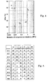
- Fig. 4 is a graph showing a relation between a modulus of compression elasticity and a jitter value of the photoresist shown in Fig. 3.
- Fig. 5 is an explanatory chart showing a mixing ratio of a base resin and photoacid generator, which is another example of an embodiment 2 of increasing a molecular weight of base resin of photoresist constituting a photoresist film according to the present invention.
- Fig. 6 is an explanatory chart showing a weight-average molecular weight (Mw), a modulus of compression elasticity and a jitter value of an optical disc being manufacture by using the photoresist shown in Fig. 5.
- Fig. 7 is a graph showing a relation between a modulus of compression elasticity and a jitter value of the photoresist shown in Fig. 6.
- Fig. 8 is an explanatory chart showing a adding ratio of photoresist and hardener available in the market, which is an embodiment 3 of adding hardener of a base resin to photoresist constituting a photoresist film according to the present invention.
- Fig. 9 is an explanatory chart showing a weight-average molecular weight (Mw), a modulus of compression elasticity and a jitter value of an optical disc being manufacture by using the photoresist shown in Fig. 8.
- Fig. 10 is a graph showing a relation between a modulus of compression elasticity and a jitter value of the photoresist shown in Fig. 9.
- Fig. 11 is an explanatory chart showing a blending ratio of photoresist and light curable resin available in the market, which is a first example of an embodiment 4 of blending a curable resin with photoresist constituting a photoresist film according to the present invention.
- Fig. 12 is an explanatory chart showing a blending ratio of photoresist and thermosetting resin available in the market, which is a second example of the embodiment 4 of blending a curable resin with photoresist constituting a photoresist film according to the present invention.
- Fig. 13 is an explanatory chart showing a modulus of compression elasticity and a jitter value of an optical disc being manufacture by using the photoresist shown in Fig. 11.
- Fig. 14 is an explanatory chart showing a modulus of compression elasticity and a jitter value of an optical disc being manufacture by using the photoresist shown in Fig. 12.
- Fig. 15 is a graph showing a relation between a modulus of compression elasticity and a jitter value of the photoresist shown in Fig. 13.
- Fig. 16 is a graph showing a relation between a modulus of compression elasticity and a jitter value of the photoresist shown in Fig. 14.
- Fig. 17 is an explanatory chart showing a blending ratio of photoresist and light curable resin available in the market, which is a first example of an embodiment 5 of blending a curable resin with photoresist constituting a photoresist film according to the present invention.
- Fig. 18 is an explanatory chart showing a blending ratio of photoresist and thermosetting resin available in the market, which is a second example of the embodiment 5 of blending a curable resin with photoresist constituting a photoresist film according to the present invention.
- Fig. 19 is an explanatory chart showing a modulus of compression elasticity and a jitter value of an optical disc being manufacture by using the photoresist shown in Fig. 17.
- Fig. 20 is an explanatory chart showing a modulus of compression elasticity and a jitter value of an optical disc being manufacture by using the photoresist shown in Fig. 18.
- Fig. 21 is a graph showing a relation between a modulus of compression elasticity and a jitter value of the photoresist shown in Fig. 19.
- Fig. 22 is a graph showing a relation between a modulus of compression elasticity and a jitter value of the photoresist shown in Fig. 20.
- the processes such as forming a conductive film and plating are regular processes. Therefore, it is supposed that such deformation of a shape of pit or groove has happened until now. However, deteriorating a jitter value caused by such the deformation has not emerged because a ratio of deformation amount with respect to a pit length and a track pitch is relatively small enough for an optical disc having a density of the order of 4.7 GB, for example. On the other hand, in a case of a higher density level such as more than 20 GB, as a pit length and a track pitch become shorter than those of 4.7 GB, a signal characteristic is deteriorated by the deformation even though a shape of pit or groove is slightly deformed.
- a first method of increasing a mechanical strength of photoresist is increasing a molecular weight of base resin of the photoresist.
- the cresol novolac resin is used as a base resin.
- a light source for exposure is advanced to a shorter wavelength in order to cope with higher density.
- chemical amplification type resin being commonly utilized for a wavelength of 200 to 300 nm
- increasing a molecular weight excessively will cause injurious effects upon the photoresist.
- One of such injurious effects is caused by growing a molecular size.
- a size of signal to be recorded becomes smaller with advancing an optical disc to a higher density.
- its minimum pit length is required to be approximately 0.2 to 0.25 ⁇ m.
- a molecular size of base resin constituting photoresist becomes larger, scattering of pit length caused by variation of development becomes wider and affects a jitter value. If a molecular weight of base resin becomes an order of some ten thousands, its molecular size becomes even some tens nm. The size can not be disregarded with respect to a pit length any more and becomes a level of deteriorating scattering of pit length.
- Another injurious effect is decreasing of sensitivity.
- a dissolving speed into developer becomes slower as a molecular weight of base resin increases, so that an apparent sensitivity decreases.
- the decreasing of sensitivity is a problem of production efficiency, an exposure time being necessary for one glass substrate becomes longer in accordance with advancing an optical disc to a higher density, and accordingly decreasing sensitivity too much is not preferable for improving throughput.
- a weight-average molecular weight of base resin is desirable to be less than 20000.
- a second method of increasing a mechanical strength of photoresist is making photoresist contain hardener for base resin.
- cresol novolac resin as the base resin of the naphthoquinone diazide cresol novolac family photoresist also has a property of thermosetting resin, by adding an amine family hardener such as hexamethylene-tetramine into the cresol novolac resin and heating, the cresol novolac resin cross-links three-dimensionally and becomes a resin being never solved or melted. Accordingly, a firm photoresist film, which is never deformed while filming, can be obtained by adding hardener into currently available photoresist and applying heat so as to cross-link three-dimensionally after a pit or groove is formed through exposing and developing processes.
- an amine family hardener such as hexamethylene-tetramine
- a heating temperature slightly varies by a type of hardener and a structure of the cresol novolac resin, generally, it is an order of 110 to 180 °C. In a case of less than 110 °C, curing reaction never happens. In a case of more than 180 °C, a contract amount becomes larger caused by curing reaction. Consequently, a pit size and a groove width or depth can hardly be controlled.
- An amount of hardener is preferable to be within a range of 1 to 30 weight parts with respect to 100 weight parts of solid component in photoresist. In a case of less than 1 weight part, insufficient cross-linking density fails to obtain a desired strength. In a case of more than 30 weight parts, as hardener is generally soluble in water, a solubility amount or a film reducing amount of a section not exposed while developing becomes larger and surface roughness becomes coarse. Accordingly, a noise level of signal increases.
- a third method of increasing a mechanical strength of photoresist is blending a resin such as a light curable resin and a thermosetting resin, which cross-links three-dimensionally and hardens by applying some treatment, with photoresist.
- This is a method of utilizing the conventional photoresist, which is blended with such a curable resin, as photoresist and increasing a total strength of a photoresist film by hardening only the blended component or the blended curable resin through irradiating the UV ray or heating after exposing and developing.
- the blending ratio is desirable to be within a range of 5 to 40 weight parts with respect to 100 weight parts of a solid component in photoresist. In a case of less than 5 weight parts, a desired strength of photoresist can be never obtained. In a case of more than 40 weight parts, it causes a defect such that resolution or sensitivity decreases as photoresist.
- Fig. 2 is an explanatory table showing a mixing ratio of cresol novolac resin and photosensitive agent, which is one example of an embodiment 1 of increasing a molecular weight of base resin of photoresist constituting a photoresist film according to the present invention.
- Fig. 3 is an explanatory chart showing a weight-average molecular weight (Mw), a modulus of compression elasticity and a jitter value of an optical disc being manufacture by using the photoresist shown in Fig. 2.
- Fig. 4 is a graph showing a relation between a modulus of compression elasticity and a jitter value of the photoresist shown in Fig. 3.
- positive photoresist utilized for a wavelength range of the order of 340 to 460 nm is composed of cresol novolac resin and benzophenone ester of modified naphthoquinone diazide as photosensitive agent, which are dissolved in a solvent together.
- a synthesizing example of cresol novolac resin is as follows: pour distilled m-cresol and p-cresol in the proportion 1:1 into a separable flask having three mouths equipped with a circulating cooling tube and a thermometer, add 74 grams of a solution of 37 % formaldehyde and 2.3 grams of oxalic acid dihydrate into the flask, heat a total solution in the oil bath with agitating the total solution and react the total solution for a period of 15 hours at a reflux temperature.
- cresol novolac resin obtained as mentioned above is divided into 5 fractions extending from a component in high molecular weight to a component in low molecular weight through the serial precipitation fraction method by using the ethyl cellosolve as a solvent and water as a precipitant. Consequently, 5 cresol novolac resins "A” through "E” are obtained.
- a weight-average molecular weight of each resin is measured by the gel permeation chromatography (GPC) method of standardizing polystyrene.
- a first synthesizing example of photosensitive agent is as follows: fill 10 grams of 2-, 3-, 4- and 4'-tetrahydroxy benzophenone, 40 grams of 1- and 2-naphthoquinone diazide-5-sulfonyle chloride and 300 ml of ⁇ -butyrolactone in a separable flask having three mouths and dissolve well. Drop a mixed solution of 20 grams of triethyl amine and 50 ml of acetone into the flask gradually and react with agitating the total solution for a period of 5 hours at room temperature.
- a second synthesizing example of photosensitive agent is as follows: fill 20 grams of 2-, 3- and 4-tetrahydroxy benzophenone, 50 grams of 1- and 2-naphthoquinone diazide-5-sulfonyle chloride and 250 ml of dioxane in a separable flask having three mouths and dissolve well. Drop 15 grams of triethyl amine into the flask gradually and react with agitating the total solution for a period of 4 hours at room temperature. Treat the total solution as the same process as the first example mentioned above. Then a benzophenone ester "G" is obtained. 3-substitution product occupies 80 % of total dehydrated deposit when analyzing the deposit as the same manner as the first synthesizing example.
- Compounding photoresist is as follows: mix each of the cresol novolac resins "A” through “E” obtained as mentioned above, the benzophenone ester “F” obtained by the first synthesizing example of photosensitive agent and the benzophenone ester “G” obtained by the second synthesizing example of photosensitive agent in accordance with a ratio shown in Fig. 2 and dissolve the mixture in a solvent. Consequently, each of photoresist #1 through #10 is obtained by filtrating the dissolved mixture through a 0.2 ⁇ m filter. Further, with respect to a solvent, 2-heptanone is used for a solvent and its consistency is compounded so as to enable to obtain a desired film thickness by the spin coat method.
- the photoresist #1 (2) synthesized as mentioned above is coated on a surface of disc shaped glass substrate 1, which is polished finely and washed, by the spin coat method through an adhesive, and then the entire glass substrate 1 coated with the photoresist 2 is baked in an oven (not shown) for a period of 45 minutes at 80 °C so as to remove a solvent.
- a film thickness of the photoresist 2 is designated to be slightly thicker than 750 ⁇ so as for an actual thickness of the photoresist 2 after development to be 750 ⁇ .
- a signal to be recorded is a group of pits of which a track pitch is 0.4 ⁇ m and a pit length is 3T to 11T if a minimum pit length 3T is 0.254 ⁇ m.
- a laser power is selected such that a jitter value becomes minimal in response to a sensitivity of the photoresist #1.
- the exposed area 5 is dissolved and a glass master having a roughened photoresist pattern 6 composed of a group of pits is obtained.
- a stamper 7 is manufactured by plating nickel over the glass master.
- a polycarbonate resin 8 is injected into the stamper 7.
- a reflection film 9 is formed on the surface of the polycarbonate resin 8 and further a protective film 10 is formed over the reflection film 9; and finally an optical disc D1 is obtained.
- the reflection film 9 is composed of aluminum having a film thickness of 700 ⁇ .
- optical disc D1 manufactured by using the photoresist #1 is explained.
- photoresist #2 through #10 an optical disc is manufactured by using each of the photoresist #2 through #10 as each of optical discs D2 through D10 respectively.
- an optical disc E1 is manufactured as a comparative example through the same process as the optical disc D1.
- each optical disc manufactured as mentioned above is reproduced by using a laser pickup having a wavelength of 405 nm and a numerical aperture NA of 0.75.
- An reproduced output is analyzed by using a time interval analyzer and a jitter value is obtained from a signal distribution corresponding to each pit of a frequency characteristic curve.
- a frequency distribution per time is obtained and a jitter value is a standardized value, which is obtained by dividing a standard deviation of change of time base of the distribution by a period corresponding to 1T.
- a jitter value exceeds 15 %, pit separation margin while reproducing decreases and it becomes impractical.
- a C1 error increases and it may be hard to reproduce continuously.
- a measuring method of a modulus of compression elasticity exhibiting a mechanical strength of photoresist is explained next.
- Each of the photoresist #1 through #10 and the conventional photoresist S1 dissolved in a solvent (2-heptanone) is dropped into an aluminum pan having a diameter of 7 mm and a depth of 1.2 mm and dehydrated in a vacuum at 80 °C.
- consistency of photoresist can be determined arbitrarily and they shall be dehydrated in a low temperature and a low vacuum in order to prevent them from bubbling up.
- Repeating these operations of dropping and dehydrating several times fills the aluminum pan with the photoresist as much as the photoresist rises from the edge of aluminum pan.
- the surface of the photoresist is filed off so as to be flat and the surface height is arranged to be the same height as the aluminum pan after it is sufficiently dehydrated and a solvent is completely volatilized. Accordingly, samples for measurement are obtained.
- the samples obtained as mentioned above are measured their moduli of compression elasticity at 100 °C by using the thermo mechanical analyzer, model TMA/SS10 manufactured by Seiko Instruments Inc. Applying a compression stress of 1.0 ⁇ 0.5 g sinusoidally by a circular prove made by quartz having a contact area of 4.2 mm 2 while increasing an ambient temperature from a room temperature to approximately 150 °C to each sample obtains a modulus of compression elasticity at 100 °C by measuring a distortion amount at a moment.
- each of the optical disc D1 through D10 is manufactured.
- a result of evaluation is shown in Fig. 3.
- Fig. 3 a weight-average molecular weight Mw of the base resin or the cresol novolac resin, a modulus of compression elasticity at 100 °C and a jitter value with respect to each sample of the photoresist #1 through #10 and S1 is listed.
- Fig. 4 a relation between a modulus of compression elasticity at 100 °C of photoresist and a jitter value is exhibited. It exhibits the contents of Fig. 3 graphically. According to Fig.
- a jitter value is less than 15 % within a range of 8.0 ⁇ 10 -3 to 5.0 ⁇ 10 -1 MPa of modulus of compression elasticity of photoresist at 100 °C.
- a molecular weight of the base resin at the minimum and maximum values is 8040 and 19500 respectively.
- Fig. 5 is an explanatory chart showing a mixing ratio of a base resin and photoacid generator, which is another example of an embodiment 2 of increasing a molecular weight of base resin of photoresist constituting a photoresist film according to the present invention.
- Fig. 6 is an explanatory chart showing a weight-average molecular weight (Mw), a modulus of compression elasticity and a jitter value of an optical disc being manufacture by using the photoresist shown in Fig. 5.
- Fig. 7 is a graph showing a relation between a modulus of compression elasticity and a jitter value of the photoresist shown in Fig. 6.
- chemical amplification type positive photoresist utilized for a wavelength range of the order of 200 to 300 nm is composed of a resin of hydroxyl group of polyhydroxy styrene protected by a protective group such as tert-butoxy carbonyl group as a base resin and an photoacid generator such as sulfonium salt as a photosensitive agent. Therefore, chemical amplification type positive photoresist containing these chemicals is manufactured.
- a synthesizing example of a base resin is as follows: in a flask having four mouths displaced by nitrogen, dissolve 50 grams of polyhydroxy styrene resin (Trade name: Marukalinker-M manufactured by Maruzen Petrochemical Co., Ltd.) in 200 ml of acetone, add 17.63 grams of potassium carbonate, 8.48 grams of potassium iodide and 24.38 grams of tert-butyl bromo acetate into the solution and reflux for a period of 7 hours with agitating the total solution.
- polyhydroxy styrene resin (Trade name: Marukalinker-M manufactured by Maruzen Petrochemical Co., Ltd.) in 200 ml of acetone, add 17.63 grams of potassium carbonate, 8.48 grams of potassium iodide and 24.38 grams of tert-butyl bromo acetate into the solution and reflux for a period of 7 hours with agitating the total solution.
- the solution is dropped into 1500 ml of water and a polymer is deposited.
- the polymer is filtered out and dehydrated by wind for a period of 12 hours after being rinsed 5 times with 300 ml of water.
- the dehydrated polymer is dissolved in 220 ml of ethanol once again and precipitated and refined through similar processes as mentioned above, and then an objective polymer of which weight is 52.0 grams is obtained after dehydrating for a period of 24 hours in a vacuum dryer at 50 °C.
- the objective polymer is found that 35 % of hydroxy group in the polyhydroxy styrene changes into the tert-butoxy carbonyl methyl ether.
- the objective polymer or a base resin synthesized as mentioned above is divided into 5 fractions extending from a component in high molecular weight to a component in low molecular weight through the serial precipitation fraction method by using the ethyl cellosolve as a solvent and water as a precipitant. Consequently, 5 base resins "H” through “L” are obtained.
- a weight-average molecular weight of each resin is measured by the GPC (gel permeation chromatography) method of standardizing polystyrene.
- Compounding photoresist is as follows: mix each of the base resins "H” through “L” obtained as mentioned above and triphenyl sulfonium trifrate "M" of photoacid generator in accordance with a ratio shown in Fig. 5 and dissolve the mixture in a solvent. Consequently, each of photoresist #11 through #20 is obtained by filtrating the dissolved mixture through a 0.2 ⁇ m filter. Further, with respect to a solvent, propylene glycol monomethyl ether acetate is used for a solvent and its consistency is compounded so as to enable to obtain a desired film thickness by the spin coat method.
- respective optical discs D11 through D20 are manufactured and a jitter characteristic of each disc is evaluated.
- Manufacturing processes of an optical disc is identical to those of the embodiment 1, so that only a manufacturing method being different from that of the embodiment 1 is explained next.
- the photoresist #11 is coated on a quartz glass substrate by using the same method as the embodiment 1.
- a YAG quadruple wave laser beam having a wavelength of 266 nm, which is modulated by a signal to be recorded, is condensed by a lens, irradiated on the surface of the photoresist #11 and exposes a predetermined area or an exposed area of the photoresist #11 with allowing a predetermined period of time.
- a signal to be recorded is a group of pits of which a track pitch is 0.34 ⁇ m and a pit length is 3T to 11T if a minimum pit length 3T is 0.19 ⁇ m.
- a laser power is selected such that a jitter value becomes minimal in response to a sensitivity of the photoresist #11.
- optical disc D11 manufactured by using the photoresist #11 is explained.
- photoresist #12 through #20 an optical disc is manufactured by using each of the photoresist #12 through #20 as each of optical discs D12 through D20 respectively.
- an optical disc E2 is manufactured as a comparative example through the same process as the optical disc D11.
- the optical discs D11 through D20 and E2 manufactured as mentioned above are evaluated by the same method as the embodiment 1.
- a result of the evaluation is shown in Fig. 6, and further its resultant is graphed in Fig. 7.
- Fig. 7 a relation between a modulus of compression elasticity at 100 °C of photoresist and a jitter value is exhibited.
- a jitter value is less than 15 % within a range of 8.0 ⁇ 10 -3 to 5.0 ⁇ 10 -1 MPa of modulus of compression elasticity of photoresist at 100 °C.
- a molecular weight of the base resin at the minimum and maximum values is 8150 and 19100 respectively.
- Fig. 8 is an explanatory chart showing a adding ratio of photoresist and hardener available in the market, which is an embodiment 3 of adding hardener of a base resin to photoresist constituting a photoresist film according to the present invention.
- Fig. 9 is an explanatory chart showing a weight-average molecular weight (Mw), a modulus of compression elasticity and a jitter value of an optical disc being manufacture by using the photoresist shown in Fig. 8.
- Fig. 10 is a graph showing a relation between a modulus of compression elasticity and a jitter value of the photoresist shown in Fig. 9.
- HMT hexamethylentetramine
- S3 naphthoquinone diazide - cresol novolac family photoresist on the market
- a blended solvent containing 90 % of ester lactate and 10 % of butyl acetate is used for a solvent and its consistency is compounded so as to enable to obtain a desired film thickness by the spin coat method.
- an additive amount shown in Fig. 8 is exhibited as a ratio of a component weight to a weight of resin solid component in photoresist, which is defined to be 100 weight parts.
- respective optical discs D21 through D27 are manufactured and a jitter characteristic of each disc is evaluated.
- Manufacturing processes of each optical disc is identical to those of the embodiment 1, so that only a manufacturing method being different from that of the embodiment 1 is explained next.
- the photoresist #21 is coated on a green glass substrate by the same method as the embodiment 1.
- a Kr-laser beam having a wavelength of 351 nm, which is modulated by a signal to be recorded, is condensed by a lens, and irradiated on the surface of the photoresist #21 and exposes a predetermined area or a exposed area of the photoresist #21 with allowing a predetermined period of time.
- a signal to be recorded is a group of pits of which a track pitch is 0.4 ⁇ m and a pit length is 3T to 11T if a minimum pit length 3T is 0.254 ⁇ m.
- a laser power is selected such that a jitter value becomes minimal in response to a sensitivity of the photoresist #21.
- a glass master having a roughened photoresist pattern composed of a group of pits is obtained.
- a stamper and an optical disc D21 is obtained from the glass master by using the same method as the embodiment 1.
- optical disc D21 manufactured by using the photoresist #21 is explained.
- photoresist #22 through #27 an optical disc is manufactured by using each of the photoresist #22 through #27 as each of optical discs D22 through D27.
- the optical discs D21 through D27 manufactured as mentioned above are evaluated by the same method as the embodiment 1.
- a result of the evaluation is shown in Fig. 9, and further its resultant is graphed in Fig. 10.
- Fig. 10 a relation between a modulus of compression elasticity at 100 °C of photoresist and a jitter value is exhibited. According to Fig. 10, it is confirmed that a jitter value is less than 15 % within a range of 8.0 ⁇ 10 -3 to 5.0 ⁇ 10 -1 MPa of modulus of compression elasticity of photoresist at 100 °C.
- Fig. 11 is an explanatory chart showing a blending ratio of photoresist and light curable resin available in the market, which is a first example of an embodiment 4 of blending a curable resin with photoresist constituting a photoresist film according to the present invention.
- Fig. 12 is an explanatory chart showing a blending ratio of photoresist and thermosetting resin available in the market, which is a second example of an embodiment 4 of blending a curable resin with photoresist constituting a photoresist film according to the present invention.
- Fig. 13 is an explanatory chart showing a modulus of compression elasticity and a jitter value of an optical disc being manufacture by using the photoresist shown in Fig. 11.
- Fig. 14 is an explanatory chart showing a modulus of compression elasticity and a jitter value of an optical disc being manufacture by using the photoresist shown in Fig. 12.
- Fig. 15 is a graph showing a relation between a modulus of compression elasticity and a jitter value of the photoresist shown in Fig. 13.
- Fig. 16 is a graph showing a relation between a modulus of compression elasticity and a jitter value of the photoresist shown in Fig. 14.
- Compounding photoresist is as follows: blend trimethylol propane triaclylete (containing 10 % of photo initiator, referred to as "TMPTA” in Fig. 11) as a light curable resin and TB-3042 (manufactured by Three Bond Co., Ltd., referred to as "TB” in Fig. 12) as a thermosetting resin with the naphthoquinone diazide - cresol novolac family photoresist on the market (trade name: THMR-AR80 manufactured by Tokyo Ohka Kogyo Co., Ltd., referred to as "S4" in Fig. 11) in accordance with a ratio shown in Figs. 11 and 12, and dilute the mixture in a solvent.
- each of photoresist #28 through #41 is obtained by filtrating the diluted mixture through a 0.2 ⁇ m filter.
- a blended solvent containing 90 % of ester lactate and 10 % of butyl acetate is used for a solvent and its consistency is compounded so as to enable to obtain a desired film thickness by the spin coat method.
- an additive amount shown in Figs. 11 and 12 is exhibited as a ratio of a component weight to a weight of resin solid component in photoresist, which is defined to be 100 weight parts.
- respective optical discs D28 through D41 are manufactured and a jitter characteristic of each disc is evaluated. Manufacturing processes of the optical discs are identical to those of the embodiment 1, so that only a manufacturing method being different from that of the embodiment 1 is explained next.
- the photoresist is coated on a green glass substrate by the same method as the embodiment 1.
- a Kr-laser beam having a wavelength of 351 nm, which is modulated by a signal to be recorded, is condensed by a lens, and irradiated on the surface of the photoresist and exposes a predetermined area or a exposed area of the photoresist with allowing a predetermined period of time.
- a signal to be recorded is a group of pits of which a track pitch is 0.4 ⁇ m and a pit length is 3T to 11T if a minimum pit length 3T is 0.254 ⁇ m.
- a laser power is selected such that a jitter value becomes minimal in response to a sensitivity of the photoresist.
- a stamper and an optical disc are obtained from the glass master by using the same method as the embodiment 1.
- each of the optical discs D29 through D41 is manufactured by using each of the photoresist #29 through #41 respectively by the same processes as the optical disc D28.
- FIGs. 15 and 16 A result of the evaluation is shown in Figs. 13 and 14, and further its resultant is graphed in Figs. 15 and 16 respectively.
- a relation between a modulus of compression elasticity at 100 °C of photoresist and a jitter value is exhibited.
- a jitter value is less than 15 % within a range of 8.0 x 10 -3 to 5.0 ⁇ 10 -1 MPa of modulus of compression elasticity of photoresist at 100 °C.
- Fig. 17 is an explanatory chart showing a blending ratio of photoresist and light curable resin available in the market, which is a first example of an embodiment 5 of blending a curable resin with photoresist constituting a photoresist film according to the present invention.
- Fig. 18 is an explanatory chart showing a blending ratio of photoresist and thermosetting resin available in the market, which is a second example of the embodiment 5 of blending a curable resin with photoresist constituting a photoresist film according to the present invention.
- Fig. 19 is an explanatory chart showing a modulus of compression elasticity and a jitter value of an optical disc being manufacture by using the photoresist shown in Fig. 17.
- Fig. 20 is an explanatory chart showing a modulus of compression elasticity and a jitter value of an optical disc being manufacture by using the photoresist shown in Fig. 18.
- Fig. 21 is a graph showing a relation between a modulus of compression elasticity and a jitter value of the photoresist shown in Fig. 19.
- Fig. 22 is a graph showing a relation between a modulus of compression elasticity and a jitter value of the photoresist shown in Fig. 20.
- Compounding photoresist is as follows: blend trimethylol propane triaclylete (containing 10 % of photo initiator, referred to as "TMPTA” in Fig. 17) as a light curable resin and TB-3042 (manufactured by Three Bond Co., Ltd., referred to as "TB” in Fig. 18) as a thermosetting resin with the chemical amplification type photoresist on the market (trade name: TDUR-P308 manufactured by Tokyo Ohka Kogyo Co., Ltd., referred to as "S5" in Figs. 17 and 18) in accordance with a ratio shown in Figs. 17 and 18, and dilute the mixture in a solvent.
- each of photoresist #42 through #55 is obtained by filtrating the diluted mixture through a 0.2 ⁇ m filter.
- propylene glycol monomethyl ether acetate is used for a solvent and its consistency is compounded so as to enable to obtain a desired film thickness by the spin coat method.
- a blending amount shown in Figs. 17 and 18 is exhibited as a ratio of a component weight to a weight of resin solid component in photoresist, which is defined to be 100 weight parts.
- respective optical discs D42 through D55 are manufactured by using the same method as the embodiment 2.
- Each optical disc is formed with a group of pits of which a track pitch is 0.34 ⁇ m and a pit length is 3T to 11T, wherein a minimum pit length 3T is 0.19 ⁇ m.
- TMPTA light curable resin
- thermosetting resin "TB” thermosetting resin
- the optical discs D42 through D55 manufactured as mentioned above are evaluated by the same method as the embodiment 1.
- a result of the evaluation is shown in Figs. 19 and 20, and further its resultant is graphed in Figs. 21 and 22.
- a jitter value is less than 15 % within a range of 8.0 ⁇ 10 -3 to 5.0 ⁇ 10 -1 MPa of modulus of compression elasticity of photoresist at 100 °C.
- uniformity of groove width is one of the most important factors affecting quality of a reproduced signal characteristic even in a rewritable information recording medium having a continuous groove.
- Increasing a mechanical strength of photoresist can control scattering of groove width. Therefore, the manufacturing method of information recording medium according to the present invention can be applied to a rewritable information recording medium having a continuous groove.
- a wavelength of a laser beam for exposure is exemplified by 351 nm and 266 nm.
- a wavelength is not limited to them.
- several methods are exemplified as a method of increasing a mechanical strength of photoresist. Nevertheless, a method of increasing a mechanical strength of photoresist is not limited to the methods mentioned in the embodiments.
- a positive photoresist utilized for manufacturing an information recording medium, which is recorded with an information signal formed as a pit or a groove on a disc.
- a modulus of compression elasticity of a solid component of the photoresist after removing a solvent component is set to be within a range of 8.0 ⁇ 10 -3 to 5.0 ⁇ 10 -1 MPa at 100 °C, so that deformation of a pit or a groove can be reduced in a succeeding process. Accordingly, a high density information recording medium in high quality such as small in jitter value can be provided.
- a manufacturing method of an information recording medium by making use of the above-mentioned positive photoresist comprises a a step of forming a film of positive photoresist mentioned above, a step of forming a latent image by irradiating a laser beam on the photoresist film, a step of forming a pit or a groove pattern by developing the latent image by an alkaline aqueous solution, a step of producing a stamper by plating a metal on the pit or the groove pattern and a step of duplicating a plastic substrate formed with the pit or the groove pattern by using the stamper.
- a mechanical strength of photoresist can be improved, so that deformation of a pit or a groove can be reduced in a succeeding process. Accordingly, a high density information recording medium in high quality such as small in jitter value can be provided.
- an information recording medium manufactured by the above-mentioned manufacturing method, which is in high density and in higher quality being small in jitter value.
Landscapes
- Physics & Mathematics (AREA)
- Spectroscopy & Molecular Physics (AREA)
- General Physics & Mathematics (AREA)
- Engineering & Computer Science (AREA)
- Manufacturing & Machinery (AREA)
- Manufacturing Optical Record Carriers (AREA)
- Materials For Photolithography (AREA)
Applications Claiming Priority (2)
| Application Number | Priority Date | Filing Date | Title |
|---|---|---|---|
| JP2000378513A JP2002184043A (ja) | 2000-12-13 | 2000-12-13 | 情報記録担体用ポジ型フォトレジスト、情報記録担体の製造方法および情報記録担体 |
| JP2000378513 | 2000-12-13 |
Publications (1)
| Publication Number | Publication Date |
|---|---|
| EP1225476A1 true EP1225476A1 (de) | 2002-07-24 |
Family
ID=18847070
Family Applications (1)
| Application Number | Title | Priority Date | Filing Date |
|---|---|---|---|
| EP01310212A Withdrawn EP1225476A1 (de) | 2000-12-13 | 2001-12-06 | Positiv-Photoresist zur Herstellung von einem Informationsaufzeichnungsmedium, Verfahren zur Herstellung von einem Informationsaufzeichnungsmedium und ein Informationsaufzeichnungsmedium |
Country Status (3)
| Country | Link |
|---|---|
| US (1) | US20020071929A1 (de) |
| EP (1) | EP1225476A1 (de) |
| JP (1) | JP2002184043A (de) |
Families Citing this family (4)
| Publication number | Priority date | Publication date | Assignee | Title |
|---|---|---|---|---|
| JP4492393B2 (ja) * | 2005-03-08 | 2010-06-30 | チッソ株式会社 | 感光性組成物およびそれを用いた表示素子 |
| JP4647542B2 (ja) * | 2006-05-15 | 2011-03-09 | シャープ株式会社 | 微細パターンの形成方法 |
| FR2929749A1 (fr) * | 2008-04-08 | 2009-10-09 | Pascal Andre | Procede et systeme pour l'enregistrement de donnees sous forme d'une nanostructure |
| CN105474096B (zh) | 2013-08-27 | 2019-11-12 | 日本瑞翁株式会社 | 辐射敏感树脂组合物、树脂膜及电子部件 |
Citations (6)
| Publication number | Priority date | Publication date | Assignee | Title |
|---|---|---|---|---|
| EP0561079A1 (de) * | 1992-03-16 | 1993-09-22 | Pioneer Electronic Corporation | Photoresist für optische Platte und Verfahren zur Herstellung optischer Platten unter Verwendung des Photoresists |
| EP0561080A1 (de) * | 1992-03-16 | 1993-09-22 | Pioneer Electronic Corporation | Photoresist für optische Platte und Verfahren zur Herstellung optischer Platten unter Verwendung des Photoresists |
| EP0596439A2 (de) * | 1992-11-05 | 1994-05-11 | Matsushita Electric Industrial Co., Ltd. | Verfahren zur Erzeugung einer Originalplatte zum Herstellen von optischen Platten |
| JPH0764277A (ja) * | 1993-08-25 | 1995-03-10 | Toyobo Co Ltd | 感光性樹脂凸版材 |
| EP0875891A2 (de) * | 1997-05-01 | 1998-11-04 | Kabushiki Kaisha Toshiba | Informationsaufzeichnungsmedium, Schneidegerät und Informationswiedergabegerät |
| JPH11102541A (ja) * | 1997-09-29 | 1999-04-13 | Sony Corp | 光ディスク用原盤の製造方法 |
-
2000
- 2000-12-13 JP JP2000378513A patent/JP2002184043A/ja active Pending
-
2001
- 2001-12-06 EP EP01310212A patent/EP1225476A1/de not_active Withdrawn
- 2001-12-13 US US10/013,504 patent/US20020071929A1/en not_active Abandoned
Patent Citations (7)
| Publication number | Priority date | Publication date | Assignee | Title |
|---|---|---|---|---|
| EP0561079A1 (de) * | 1992-03-16 | 1993-09-22 | Pioneer Electronic Corporation | Photoresist für optische Platte und Verfahren zur Herstellung optischer Platten unter Verwendung des Photoresists |
| EP0561080A1 (de) * | 1992-03-16 | 1993-09-22 | Pioneer Electronic Corporation | Photoresist für optische Platte und Verfahren zur Herstellung optischer Platten unter Verwendung des Photoresists |
| EP0596439A2 (de) * | 1992-11-05 | 1994-05-11 | Matsushita Electric Industrial Co., Ltd. | Verfahren zur Erzeugung einer Originalplatte zum Herstellen von optischen Platten |
| JPH0764277A (ja) * | 1993-08-25 | 1995-03-10 | Toyobo Co Ltd | 感光性樹脂凸版材 |
| EP0875891A2 (de) * | 1997-05-01 | 1998-11-04 | Kabushiki Kaisha Toshiba | Informationsaufzeichnungsmedium, Schneidegerät und Informationswiedergabegerät |
| JPH11102541A (ja) * | 1997-09-29 | 1999-04-13 | Sony Corp | 光ディスク用原盤の製造方法 |
| US6214528B1 (en) * | 1997-09-29 | 2001-04-10 | Sony Corporation | Method of forming mother for use in optical disc |
Non-Patent Citations (1)
| Title |
|---|
| PATENT ABSTRACTS OF JAPAN vol. 1995, no. 06 31 July 1995 (1995-07-31) * |
Also Published As
| Publication number | Publication date |
|---|---|
| US20020071929A1 (en) | 2002-06-13 |
| JP2002184043A (ja) | 2002-06-28 |
Similar Documents
| Publication | Publication Date | Title |
|---|---|---|
| EP1225476A1 (de) | Positiv-Photoresist zur Herstellung von einem Informationsaufzeichnungsmedium, Verfahren zur Herstellung von einem Informationsaufzeichnungsmedium und ein Informationsaufzeichnungsmedium | |
| US20030002429A1 (en) | Optical information recording medium, stamper, and method of stamper manufacture | |
| CN1248214C (zh) | 光信息记录媒体及其制造方法 | |
| US6504815B1 (en) | Optical information medium, stamper for manufacturing transparent substrate therefor and recording method therefor | |
| JP3001077B2 (ja) | 情報記録担体用フォトレジスト及び情報記録担体 | |
| JP3001076B2 (ja) | 情報記録担体用フォトレジスト及び情報記録担体 | |
| JPH0636353A (ja) | バイポーラ光学記憶装置およびその製造方法 | |
| US20060246378A1 (en) | Photolithographic process, stamper, use of said stamper and optical data storage medium | |
| JP2000021031A (ja) | 光記録媒体の原盤製造法 | |
| JPH10241214A (ja) | 光ディスク用スタンパーの製造方法 | |
| KR20050021313A (ko) | 광 정보 기록 매체의 원반 제조 방법, 패턴 형성 방법,원반, 스탬퍼, 광 정보 기록 매체 및 레지스트 | |
| JP2848992B2 (ja) | 光記録媒体及びそれに用いる光記録媒体用基板 | |
| JP2001005175A (ja) | 情報記録媒体用フォトレジスト | |
| JP2005032317A (ja) | 光学記録再生媒体、光学記録再生媒体製造用スタンパ及び光学記録方法 | |
| JP2004037492A (ja) | 光ディスク用フォトレジスト | |
| JPH11350181A (ja) | スタンパの製造方法 | |
| JPH0954983A (ja) | 光記録媒体およびその製造方法 | |
| JP2005203052A (ja) | 光ディスクスタンパの作製方法、光ディスクスタンパおよび光ディスク | |
| JP2005293631A (ja) | スタンパの製造方法及び光ディスク基板の製造方法 | |
| JPH048857B2 (de) | ||
| JPH10124935A (ja) | 光ディスク用スタンパの作製方法 | |
| JPH06243512A (ja) | 光ディスク用原盤の作製法 | |
| JPS60258743A (ja) | 光デイスク | |
| JPH04301241A (ja) | 光ディスク製造方法 | |
| JPH0310087B2 (de) |
Legal Events
| Date | Code | Title | Description |
|---|---|---|---|
| PUAI | Public reference made under article 153(3) epc to a published international application that has entered the european phase |
Free format text: ORIGINAL CODE: 0009012 |
|
| AK | Designated contracting states |
Kind code of ref document: A1 Designated state(s): AT BE CH CY DE DK ES FI FR GB GR IE IT LI LU MC NL PT SE TR |
|
| AX | Request for extension of the european patent |
Free format text: AL;LT;LV;MK;RO;SI |
|
| 17P | Request for examination filed |
Effective date: 20020807 |
|
| AKX | Designation fees paid |
Designated state(s): DE FR GB |
|
| STAA | Information on the status of an ep patent application or granted ep patent |
Free format text: STATUS: THE APPLICATION HAS BEEN WITHDRAWN |
|
| 18W | Application withdrawn |
Effective date: 20060412 |