EP1227467A2 - Dispositif d'émission de lumière avec réglage du courant - Google Patents
Dispositif d'émission de lumière avec réglage du courant Download PDFInfo
- Publication number
- EP1227467A2 EP1227467A2 EP02001895A EP02001895A EP1227467A2 EP 1227467 A2 EP1227467 A2 EP 1227467A2 EP 02001895 A EP02001895 A EP 02001895A EP 02001895 A EP02001895 A EP 02001895A EP 1227467 A2 EP1227467 A2 EP 1227467A2
- Authority
- EP
- European Patent Office
- Prior art keywords
- oled
- oleds
- current value
- light emitting
- emitting device
- Prior art date
- Legal status (The legal status is an assumption and is not a legal conclusion. Google has not performed a legal analysis and makes no representation as to the accuracy of the status listed.)
- Granted
Links
Images


Classifications
-
- G—PHYSICS
- G09—EDUCATION; CRYPTOGRAPHY; DISPLAY; ADVERTISING; SEALS
- G09G—ARRANGEMENTS OR CIRCUITS FOR CONTROL OF INDICATING DEVICES USING STATIC MEANS TO PRESENT VARIABLE INFORMATION
- G09G3/00—Control arrangements or circuits, of interest only in connection with visual indicators other than cathode-ray tubes
- G09G3/20—Control arrangements or circuits, of interest only in connection with visual indicators other than cathode-ray tubes for presentation of an assembly of a number of characters, e.g. a page, by composing the assembly by combination of individual elements arranged in a matrix no fixed position being assigned to or needed to be assigned to the individual characters or partial characters
- G09G3/22—Control arrangements or circuits, of interest only in connection with visual indicators other than cathode-ray tubes for presentation of an assembly of a number of characters, e.g. a page, by composing the assembly by combination of individual elements arranged in a matrix no fixed position being assigned to or needed to be assigned to the individual characters or partial characters using controlled light sources
- G09G3/30—Control arrangements or circuits, of interest only in connection with visual indicators other than cathode-ray tubes for presentation of an assembly of a number of characters, e.g. a page, by composing the assembly by combination of individual elements arranged in a matrix no fixed position being assigned to or needed to be assigned to the individual characters or partial characters using controlled light sources using electroluminescent panels
- G09G3/32—Control arrangements or circuits, of interest only in connection with visual indicators other than cathode-ray tubes for presentation of an assembly of a number of characters, e.g. a page, by composing the assembly by combination of individual elements arranged in a matrix no fixed position being assigned to or needed to be assigned to the individual characters or partial characters using controlled light sources using electroluminescent panels semiconductive, e.g. using light-emitting diodes [LED]
- G09G3/3208—Control arrangements or circuits, of interest only in connection with visual indicators other than cathode-ray tubes for presentation of an assembly of a number of characters, e.g. a page, by composing the assembly by combination of individual elements arranged in a matrix no fixed position being assigned to or needed to be assigned to the individual characters or partial characters using controlled light sources using electroluminescent panels semiconductive, e.g. using light-emitting diodes [LED] organic, e.g. using organic light-emitting diodes [OLED]
- G09G3/3266—Details of drivers for scan electrodes
-
- G—PHYSICS
- G09—EDUCATION; CRYPTOGRAPHY; DISPLAY; ADVERTISING; SEALS
- G09G—ARRANGEMENTS OR CIRCUITS FOR CONTROL OF INDICATING DEVICES USING STATIC MEANS TO PRESENT VARIABLE INFORMATION
- G09G3/00—Control arrangements or circuits, of interest only in connection with visual indicators other than cathode-ray tubes
- G09G3/20—Control arrangements or circuits, of interest only in connection with visual indicators other than cathode-ray tubes for presentation of an assembly of a number of characters, e.g. a page, by composing the assembly by combination of individual elements arranged in a matrix no fixed position being assigned to or needed to be assigned to the individual characters or partial characters
- G09G3/22—Control arrangements or circuits, of interest only in connection with visual indicators other than cathode-ray tubes for presentation of an assembly of a number of characters, e.g. a page, by composing the assembly by combination of individual elements arranged in a matrix no fixed position being assigned to or needed to be assigned to the individual characters or partial characters using controlled light sources
- G09G3/30—Control arrangements or circuits, of interest only in connection with visual indicators other than cathode-ray tubes for presentation of an assembly of a number of characters, e.g. a page, by composing the assembly by combination of individual elements arranged in a matrix no fixed position being assigned to or needed to be assigned to the individual characters or partial characters using controlled light sources using electroluminescent panels
- G09G3/32—Control arrangements or circuits, of interest only in connection with visual indicators other than cathode-ray tubes for presentation of an assembly of a number of characters, e.g. a page, by composing the assembly by combination of individual elements arranged in a matrix no fixed position being assigned to or needed to be assigned to the individual characters or partial characters using controlled light sources using electroluminescent panels semiconductive, e.g. using light-emitting diodes [LED]
- G09G3/3208—Control arrangements or circuits, of interest only in connection with visual indicators other than cathode-ray tubes for presentation of an assembly of a number of characters, e.g. a page, by composing the assembly by combination of individual elements arranged in a matrix no fixed position being assigned to or needed to be assigned to the individual characters or partial characters using controlled light sources using electroluminescent panels semiconductive, e.g. using light-emitting diodes [LED] organic, e.g. using organic light-emitting diodes [OLED]
- G09G3/3225—Control arrangements or circuits, of interest only in connection with visual indicators other than cathode-ray tubes for presentation of an assembly of a number of characters, e.g. a page, by composing the assembly by combination of individual elements arranged in a matrix no fixed position being assigned to or needed to be assigned to the individual characters or partial characters using controlled light sources using electroluminescent panels semiconductive, e.g. using light-emitting diodes [LED] organic, e.g. using organic light-emitting diodes [OLED] using an active matrix
- G09G3/3233—Control arrangements or circuits, of interest only in connection with visual indicators other than cathode-ray tubes for presentation of an assembly of a number of characters, e.g. a page, by composing the assembly by combination of individual elements arranged in a matrix no fixed position being assigned to or needed to be assigned to the individual characters or partial characters using controlled light sources using electroluminescent panels semiconductive, e.g. using light-emitting diodes [LED] organic, e.g. using organic light-emitting diodes [OLED] using an active matrix with pixel circuitry controlling the current through the light-emitting element
-
- G—PHYSICS
- G09—EDUCATION; CRYPTOGRAPHY; DISPLAY; ADVERTISING; SEALS
- G09G—ARRANGEMENTS OR CIRCUITS FOR CONTROL OF INDICATING DEVICES USING STATIC MEANS TO PRESENT VARIABLE INFORMATION
- G09G3/00—Control arrangements or circuits, of interest only in connection with visual indicators other than cathode-ray tubes
- G09G3/20—Control arrangements or circuits, of interest only in connection with visual indicators other than cathode-ray tubes for presentation of an assembly of a number of characters, e.g. a page, by composing the assembly by combination of individual elements arranged in a matrix no fixed position being assigned to or needed to be assigned to the individual characters or partial characters
- G09G3/22—Control arrangements or circuits, of interest only in connection with visual indicators other than cathode-ray tubes for presentation of an assembly of a number of characters, e.g. a page, by composing the assembly by combination of individual elements arranged in a matrix no fixed position being assigned to or needed to be assigned to the individual characters or partial characters using controlled light sources
- G09G3/30—Control arrangements or circuits, of interest only in connection with visual indicators other than cathode-ray tubes for presentation of an assembly of a number of characters, e.g. a page, by composing the assembly by combination of individual elements arranged in a matrix no fixed position being assigned to or needed to be assigned to the individual characters or partial characters using controlled light sources using electroluminescent panels
- G09G3/32—Control arrangements or circuits, of interest only in connection with visual indicators other than cathode-ray tubes for presentation of an assembly of a number of characters, e.g. a page, by composing the assembly by combination of individual elements arranged in a matrix no fixed position being assigned to or needed to be assigned to the individual characters or partial characters using controlled light sources using electroluminescent panels semiconductive, e.g. using light-emitting diodes [LED]
- G09G3/3208—Control arrangements or circuits, of interest only in connection with visual indicators other than cathode-ray tubes for presentation of an assembly of a number of characters, e.g. a page, by composing the assembly by combination of individual elements arranged in a matrix no fixed position being assigned to or needed to be assigned to the individual characters or partial characters using controlled light sources using electroluminescent panels semiconductive, e.g. using light-emitting diodes [LED] organic, e.g. using organic light-emitting diodes [OLED]
- G09G3/3275—Details of drivers for data electrodes
- G09G3/3283—Details of drivers for data electrodes in which the data driver supplies a variable data current for setting the current through, or the voltage across, the light-emitting elements
-
- G—PHYSICS
- G09—EDUCATION; CRYPTOGRAPHY; DISPLAY; ADVERTISING; SEALS
- G09G—ARRANGEMENTS OR CIRCUITS FOR CONTROL OF INDICATING DEVICES USING STATIC MEANS TO PRESENT VARIABLE INFORMATION
- G09G3/00—Control arrangements or circuits, of interest only in connection with visual indicators other than cathode-ray tubes
- G09G3/20—Control arrangements or circuits, of interest only in connection with visual indicators other than cathode-ray tubes for presentation of an assembly of a number of characters, e.g. a page, by composing the assembly by combination of individual elements arranged in a matrix no fixed position being assigned to or needed to be assigned to the individual characters or partial characters
- G09G3/22—Control arrangements or circuits, of interest only in connection with visual indicators other than cathode-ray tubes for presentation of an assembly of a number of characters, e.g. a page, by composing the assembly by combination of individual elements arranged in a matrix no fixed position being assigned to or needed to be assigned to the individual characters or partial characters using controlled light sources
- G09G3/30—Control arrangements or circuits, of interest only in connection with visual indicators other than cathode-ray tubes for presentation of an assembly of a number of characters, e.g. a page, by composing the assembly by combination of individual elements arranged in a matrix no fixed position being assigned to or needed to be assigned to the individual characters or partial characters using controlled light sources using electroluminescent panels
- G09G3/32—Control arrangements or circuits, of interest only in connection with visual indicators other than cathode-ray tubes for presentation of an assembly of a number of characters, e.g. a page, by composing the assembly by combination of individual elements arranged in a matrix no fixed position being assigned to or needed to be assigned to the individual characters or partial characters using controlled light sources using electroluminescent panels semiconductive, e.g. using light-emitting diodes [LED]
- G09G3/3208—Control arrangements or circuits, of interest only in connection with visual indicators other than cathode-ray tubes for presentation of an assembly of a number of characters, e.g. a page, by composing the assembly by combination of individual elements arranged in a matrix no fixed position being assigned to or needed to be assigned to the individual characters or partial characters using controlled light sources using electroluminescent panels semiconductive, e.g. using light-emitting diodes [LED] organic, e.g. using organic light-emitting diodes [OLED]
- G09G3/3275—Details of drivers for data electrodes
- G09G3/3291—Details of drivers for data electrodes in which the data driver supplies a variable data voltage for setting the current through, or the voltage across, the light-emitting elements
-
- G—PHYSICS
- G09—EDUCATION; CRYPTOGRAPHY; DISPLAY; ADVERTISING; SEALS
- G09G—ARRANGEMENTS OR CIRCUITS FOR CONTROL OF INDICATING DEVICES USING STATIC MEANS TO PRESENT VARIABLE INFORMATION
- G09G2300/00—Aspects of the constitution of display devices
- G09G2300/04—Structural and physical details of display devices
- G09G2300/0421—Structural details of the set of electrodes
- G09G2300/0426—Layout of electrodes and connections
-
- G—PHYSICS
- G09—EDUCATION; CRYPTOGRAPHY; DISPLAY; ADVERTISING; SEALS
- G09G—ARRANGEMENTS OR CIRCUITS FOR CONTROL OF INDICATING DEVICES USING STATIC MEANS TO PRESENT VARIABLE INFORMATION
- G09G2300/00—Aspects of the constitution of display devices
- G09G2300/08—Active matrix structure, i.e. with use of active elements, inclusive of non-linear two terminal elements, in the pixels together with light emitting or modulating elements
- G09G2300/0809—Several active elements per pixel in active matrix panels
- G09G2300/0842—Several active elements per pixel in active matrix panels forming a memory circuit, e.g. a dynamic memory with one capacitor
- G09G2300/0861—Several active elements per pixel in active matrix panels forming a memory circuit, e.g. a dynamic memory with one capacitor with additional control of the display period without amending the charge stored in a pixel memory, e.g. by means of additional select electrodes
- G09G2300/0866—Several active elements per pixel in active matrix panels forming a memory circuit, e.g. a dynamic memory with one capacitor with additional control of the display period without amending the charge stored in a pixel memory, e.g. by means of additional select electrodes by means of changes in the pixel supply voltage
-
- G—PHYSICS
- G09—EDUCATION; CRYPTOGRAPHY; DISPLAY; ADVERTISING; SEALS
- G09G—ARRANGEMENTS OR CIRCUITS FOR CONTROL OF INDICATING DEVICES USING STATIC MEANS TO PRESENT VARIABLE INFORMATION
- G09G2310/00—Command of the display device
- G09G2310/06—Details of flat display driving waveforms
- G09G2310/061—Details of flat display driving waveforms for resetting or blanking
-
- G—PHYSICS
- G09—EDUCATION; CRYPTOGRAPHY; DISPLAY; ADVERTISING; SEALS
- G09G—ARRANGEMENTS OR CIRCUITS FOR CONTROL OF INDICATING DEVICES USING STATIC MEANS TO PRESENT VARIABLE INFORMATION
- G09G2320/00—Control of display operating conditions
- G09G2320/02—Improving the quality of display appearance
- G09G2320/0242—Compensation of deficiencies in the appearance of colours
-
- G—PHYSICS
- G09—EDUCATION; CRYPTOGRAPHY; DISPLAY; ADVERTISING; SEALS
- G09G—ARRANGEMENTS OR CIRCUITS FOR CONTROL OF INDICATING DEVICES USING STATIC MEANS TO PRESENT VARIABLE INFORMATION
- G09G2320/00—Control of display operating conditions
- G09G2320/02—Improving the quality of display appearance
- G09G2320/0285—Improving the quality of display appearance using tables for spatial correction of display data
-
- G—PHYSICS
- G09—EDUCATION; CRYPTOGRAPHY; DISPLAY; ADVERTISING; SEALS
- G09G—ARRANGEMENTS OR CIRCUITS FOR CONTROL OF INDICATING DEVICES USING STATIC MEANS TO PRESENT VARIABLE INFORMATION
- G09G2320/00—Control of display operating conditions
- G09G2320/02—Improving the quality of display appearance
- G09G2320/029—Improving the quality of display appearance by monitoring one or more pixels in the display panel, e.g. by monitoring a fixed reference pixel
-
- G—PHYSICS
- G09—EDUCATION; CRYPTOGRAPHY; DISPLAY; ADVERTISING; SEALS
- G09G—ARRANGEMENTS OR CIRCUITS FOR CONTROL OF INDICATING DEVICES USING STATIC MEANS TO PRESENT VARIABLE INFORMATION
- G09G2320/00—Control of display operating conditions
- G09G2320/04—Maintaining the quality of display appearance
- G09G2320/043—Preventing or counteracting the effects of ageing
-
- G—PHYSICS
- G09—EDUCATION; CRYPTOGRAPHY; DISPLAY; ADVERTISING; SEALS
- G09G—ARRANGEMENTS OR CIRCUITS FOR CONTROL OF INDICATING DEVICES USING STATIC MEANS TO PRESENT VARIABLE INFORMATION
- G09G2320/00—Control of display operating conditions
- G09G2320/06—Adjustment of display parameters
- G09G2320/0693—Calibration of display systems
-
- G—PHYSICS
- G09—EDUCATION; CRYPTOGRAPHY; DISPLAY; ADVERTISING; SEALS
- G09G—ARRANGEMENTS OR CIRCUITS FOR CONTROL OF INDICATING DEVICES USING STATIC MEANS TO PRESENT VARIABLE INFORMATION
- G09G2330/00—Aspects of power supply; Aspects of display protection and defect management
- G09G2330/02—Details of power systems and of start or stop of display operation
-
- G—PHYSICS
- G09—EDUCATION; CRYPTOGRAPHY; DISPLAY; ADVERTISING; SEALS
- G09G—ARRANGEMENTS OR CIRCUITS FOR CONTROL OF INDICATING DEVICES USING STATIC MEANS TO PRESENT VARIABLE INFORMATION
- G09G3/00—Control arrangements or circuits, of interest only in connection with visual indicators other than cathode-ray tubes
- G09G3/20—Control arrangements or circuits, of interest only in connection with visual indicators other than cathode-ray tubes for presentation of an assembly of a number of characters, e.g. a page, by composing the assembly by combination of individual elements arranged in a matrix no fixed position being assigned to or needed to be assigned to the individual characters or partial characters
- G09G3/2007—Display of intermediate tones
- G09G3/2018—Display of intermediate tones by time modulation using two or more time intervals
- G09G3/2022—Display of intermediate tones by time modulation using two or more time intervals using sub-frames
Definitions
- the organic light emitting layers specifically include a light emitting layer, a hole injecting layer, an electron injecting layer, a hole transporting layer, an electron transporting layer and the like.
- the OLED basically has a structure in which an anode/a light emitting layer/a cathode are laminated in order.
- the organic light emitting material in the organic light emitting layer is easily affected by moisture, oxygen, light and heat, and the deterioration of the organic light emitting material is promoted by these substances. Specifically, speed of the deterioration of the organic light emitting layer is influenced by a structure of a device for driving the light emitting device, a characteristic of the organic light emitting material constituting the organic light emitting layer, a material for an electrode, conditions in a manufacturing process, a method of driving the light emitting device, and the like.
- the organic light emitting material constituting the organic light emitting layer differs depending on the corresponding color of the OLED. If the organic light emitting layers of the OLEDs deteriorate at different speeds in accordance with the corresponding colors, the luminance of the OLED differs depending on the color with the lapse of time. Thus, an image having a desired color can not be displayed on the light emitting device.
- the luminance of the OLED has large temperature depending property, and thus, there has been a problem in that luminance of a display and a tone vary in accordance with the temperature in constant voltage drive.
- the present invention has been made in view of the above, and an object of the present invention is therefore to provide a light emitting device in which a change of luminance of an OLED is suppressed and a desired color display can be stably performed even when an organic light emitting layer is somewhat deteriorated or when an environmental temperature is varied.
- the present inventor directs an attention to the fact that a reduction of the luminance of the OLED due to deterioration is smaller in the latter.
- the current flowing through the OLED is called an OLED driving current (Iel) in this specification.
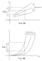
- Fig. 2 shows a change of the luminance of the OLED between a case where the OLED driving voltage is constant and a case where the OLED driving current is constant.
- the change of the luminance due to deterioration is smaller in the OLED with the constant OLED driving current. This is because not only an inclination of a straight line L-I becomes small but also a curve I-V itself moves to the lower side when the OLED is deteriorated (see Figs. 18A and 18B).
- the present inventor devised a light emitting device with a simple structure in which an OLED driving voltage can be corrected such that an OLED driving current is always kept constant even if the OLED driving current is varied due to deterioration or the like.
- variable power supply indicates a power supply in which a voltage supplied to a circuit or an element is not constant but variable in this specification.
- the light emitting device of the present invention includes a first means for measuring the OLED driving current of the OLED of the monitor pixel portion (hereinafter referred to as monitor OLED or second OLED), a second means for calculating a voltage applied to the OLED based on the measured value, and a third means for actually controlling the voltage value.
- the monitor pixel portion is input with a video signal of a different system from that of a video signal to be input to the display pixel portion.
- both the video signals are the same in the point that the signals each include gradation information, and only the system of an image to be displayed differs between the signals.
- the video signal to be input to the display pixel portion is referred to as the display video signal and the video signal to be input to the monitor pixel portion is referred to as the monitor video signal.
- the reference value of the current does not need to be fixed at the same value at all times.
- a plurality of monitor images with different reference current values are prepared, and the monitor image may be selected every monitor.
- several kinds of monitor images with the same reference current value may be prepared.
- the reduction of the luminance of the OLED can be suppressed even with the deterioration of the organic light emitting layer. As a result, a clear image can be displayed.
- a temperature of the organic light emitting layer is influenced by an outer temperature, heat generated by the OLED panel itself, or the like.
- the value of the flowing current changes in accordance with the temperature.
- Fig. 3 shows a change of a voltage-current characteristic of the OLED when the temperature of the organic light emitting layer is changed.
- the voltage is constant, if the temperature of the organic light emitting layer becomes higher, the OLED driving current becomes larger. Since the relationship between the OLED driving current and the luminance of the OLED is substantially proportional, the luminance of the OLED becomes higher as the OLED driving current becomes larger.
- the constant voltage luminance shows a vertical period for about 24 hours.
- the present invention is particularly effective for an active matrix light emitting device of digital time gradation drive, and is also effective for an active matrix light emitting device of analogue gradation drive. Further, the present invention can be applied to a passive light emitting device.
- the monitor pixel portion can be effectively used in a display of icons, logos, patterns, indicators and the like, and this can eliminate waste.
- the monitor takes the same type as the pixel, whereby the deterioration of the pixel OLED can be caught with higher definition.
- the luminance correction can be performed with ease and with accuracy.
- Fig. 1 is a block diagram of the structure of an OLED panel of the present invention.
- Reference numeral 101 denotes a display pixel portion in which a plurality of display pixels 102 are formed in matrix.
- Reference numeral 103 denotes a monitor pixel portion in which a plurality of monitor pixels 104 are formed in matrix.
- reference numerals 105 and 106 denote a source line driver circuit and a gate line driver circuit, respectively.
- the display pixel portion 101 and the monitor pixel portion 103 may be formed on the same substrate or formed on different substrates.
- the source line driver circuit 105 and the gate line driver circuit 106 are formed on the substrate on which the display pixel portion 101 and the monitor pixel portion 103 are formed in Fig. 1, the present invention is not limited to this structure.
- the source line driver circuit 105 and the gate line driver circuit 106 may be formed on the substrate different from the substrate on which the pixel portion 101 or the monitor pixel portion 103 is formed, and may be connected to the pixel portion 101 or the monitor pixel portion 103 through a connector such as an FPC.
- one source line driver circuit 105 and one gate line driver circuit 106 are provided in Fig. 1, but the present invention is not limited to this structure.
- the number of source line driver circuits 105 and the number of gate line driver circuits 106 may be arbitrarily set by a designer.
- source lines Sl to Sx, power supply lines Vl to Vx and gate lines Gl to Gy are provided in the display pixel portion 101. Then, a source line S(x+1), a power supply line V(x+1) and the gate lines Gl to Gy are provided in the monitor pixel portion 103.
- the number of source lines and the number of power supply lines are not always the same. Further, in addition to these lines, different lines may be provided.
- FIG. 1 an example in which only pixels of one line having the source line S(x+1) are provided in the monitor pixel portion 103 is shown. However, the light emitting device of the present invention is not limited to this structure. Pixels of plural lines having a plurality of source lines may be provided in the monitor pixel portion 103. The number of pixels provided in the monitor pixel portion 103 can be appropriately selected by a designer.
- Display OLEDs 107 are provided in the respective display pixels 102. Further, monitor OLEDs 108 are provided in the respective monitor pixels 104.
- the display OLED 107 and the monitor OLED 108 each have an anode and a cathode.
- the cathode is called an opposing electrode (second electrode) while, in the case where the cathode is used as a pixel electrode, the anode is called an opposing electrode.
- the pixel electrode of each of the display OLEDs 107 is connected to one of the power supply lines V1 to Vx through one TFT or a plurality of TFTs.
- the power supply lines V1 to Vx are all connected to a display variable power supply 109.
- the opposing electrodes of the display OLEDs 107 are all connected to the display variable power supply 109. Note that the opposing electrodes of the display OLEDs 107 may be connected to the display variable power supply 109 through one element or a plurality of elements.
- the pixel electrode of each of the monitor OLEDs 108 is connected to the power supply line V(x+1) through one TFT or a plurality of TFTs.
- the power supply line V(x+1) is connected to a monitor variable power supply 110 through an ammeter 111.
- the opposing electrodes of the monitor OLEDs 108 are all connected to the monitor variable power supply 110. Note that the opposing electrodes of the monitor OLEDs 108 may be connected to the monitor variable power supply 110 through one element or a plurality of elements.
- the display variable power supply 109 and the monitor variable power supply 110 are connected such that the power supply line side is kept at a high potential (Vdd) while the opposing electrode side is kept at a low potential (Vss).
- Vdd high potential
- Vss low potential
- the present invention is not limited to this structure, and the display variable power supply 109 and the monitor variable power supply 110 may be connected such that the current flown through the display OLED 107 and the monitor OLED 108 has a forward bias.
- a position where the ammeter 111 is provided is not necessarily located between the monitor variable power supply 110 and the power supply lines.
- the position may be located between the monitor variable power supply 110 and the opposing electrodes.
- Reference numeral 112 denotes a correction circuit which controls the display variable power supply 109 and the monitor variable power supply 110 based on a current value (measured value) measured with the ammeter 111. Specifically, the correction circuit 112 controls the voltage supplied to the opposing electrodes of the display OLEDs 107 and the power supply lines Vl to Vx from the display variable power supply 109 and the voltage supplied to the opposing electrodes of the monitor OLEDs 108 and the power supply line V(x+1) from the monitor variable power supply 110.
- the ammeter 111, the display variable power supply 109, the monitor variable power supply 110 and the correction circuit 112 may be formed on the substrate different from the substrate on which the display pixel portion 101 and the monitor pixel portion 103 are formed, and may be connected to the display pixel portion 101 and the monitor pixel portion 103 through a connector or the like. If possible, the above-described components may be formed on the same substrate as the display pixel portion 101 and the monitor pixel portion 103.
- a display variable power supply, a monitor variable power supply, a correction circuit and an ammeter may be provided for each color, and an OLED driving voltage may be corrected in the OLED of each color.
- the correction circuit may be provided for each color, or the common correction circuit may be provided for the OLEDs of plural colors.
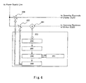
- Fig. 4 shows the detailed structure of the monitor pixel 104. Note that the display pixel 102 has the same device connection structure as the monitor pixel 104.
- the pixel structure shown in Fig. 4 is just one example, and the number of lines and elements of the pixel, the kind thereof and the connection are not limited to those in the structure shown in Fig. 4.
- the light emitting device of the present invention may take any structure provided that the OLED driving voltage of the OLED of each pixel can be controlled by the variable power supply.
- a gate electrode of the switching TFT 120 is connected to the gate line Gj.
- One of a source region and a drain region of the switching TFT 120 is connected to the source line S(x+1), and the other is connected to a gate electrode of the driving TFT 121.
- one of a source region and a drain region of the driving TFT 121 is connected to the power supply line V(x+1), and the other is connected to the pixel electrode of the monitor OLED 108.
- the capacitor 122 is formed between the gate electrode of the driving TFT 121 and the power supply line V(x+1).
- the potential of the gate line Gj is controlled by the gate line driver circuit 106, and the source line S(x+1) is input with a monitor video signal by the source line driver circuit 105.
- the switching TFT 120 is turned on, the monitor video signal input to the source line S(x+1) is input to the gate electrode of the driving TFT 121 through the switching TFT 120.
- the driving TFT 121 is turned on in accordance with the monitor video signal, the OLED driving voltage is applied between the pixel electrode and the opposing electrode of the monitor OLED 108 by the monitor variable power supply 110.
- the monitor OLED 108 emits light.
- a current is measured with the ammeter 111.
- the measured value as data is sent to the correction circuit 112.
- the period for the measurement of the current differs depending on a performance of the ammeter 111, and the period needs to have the length equal to or longer than that of the period during which the measurement can be performed. Further, with the ammeter 111, the average value or the maximum value of the current flowing in the measurement period is made to be read.
- the correction circuit 112 the measured value of the current and a set current value (reference value) are compared. Then, in the case where there is some difference between the measured value and the reference value, the correction circuit 112 controls the monitor variable power supply 110 and the display variable power supply 109, and corrects the voltage between the power supply line V(x+1) and the opposing electrode of the monitor OLED 108 and the voltage between the power supply lines Vl to Vx and the opposing electrodes of the display OLEDs 107. Thus, the OLED driving voltages in the display OLED 107 and the monitor OLED 108 are corrected, and an OLED driving current with a desired size flows.
- the OLED driving voltage may be corrected by controlling the potential at the power supply line side or may be corrected by controlling the potential at the opposing electrode side. Further, the OLED driving voltage may be corrected by controlling both the potential at the power supply line side and the potential at the opposing electrode side.
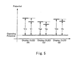
- Fig. 5 shows a change of the OLED driving voltage of the OLED of each color in the case where the potential at the power supply line side is controlled in a color light emitting device.
- Vr indicates the OLED driving voltage before correction in a display OLED (R) for R
- Vr o indicates the OLED driving voltage after correction
- Vg indicates the OLED driving voltage before correction in a display OLED (G) for G
- Vg o indicates the OLED driving voltage after correction
- Vb indicates the OLED driving voltage before correction in a display OLED (B) for B
- Vb o indicates the OLED driving voltage after correction.
- the potentials of the opposing electrodes are fixed at the same level in all of the display OLEDs.
- the OLED driving current is measured for every display OLED of each color, and the potential of the power supply line (power supply potential) is controlled by the display variable power supply, whereby the OLED driving voltage is corrected.
- variable power supplies that is, the display variable power supply corresponding to the display pixel portion and the monitor variable power supply corresponding to the monitor pixel portion are used in Fig. 1, but the present invention is not limited to this structure.
- One variable power supply may be substituted for the display variable power supply and the monitor variable power supply.
- the change of the luminance of the OLED can be suppressed even if the temperature of the organic light emitting layer is influenced by the outer temperature, the heat generated by the OLED panel itself, or the like. Also, the increase in power consumption with the temperature rise can be prevented. Further, in case of the light emitting device with the color display, the change of the luminance of the OLED of each color can be suppressed without being influenced by the temperature change. Thus, the balance of the luminance among the respective colors is prevented from being lost, and a desired color can be displayed.
- a current value (measured value) measured with an ammeter 201 is input to the A/D converter circuit 204 of the correction circuit 203.
- an analogue measured value is converted into a digital one.
- Digital data of the converted measured value is input to the memory for measured value 205 to be held.
- digital data of the reference value of an OLED driving current is held in the memory for reference value 207.
- the digital data of the measured value held in the memory for measured value 205 and the digital data of the reference value held in the memory for reference value 207 are read out to be compared.
- a monitor variable power supply 202 and a display variable power supply 209 are controlled in order to make the value of the current actually flowing through the ammeter 201 close to the reference value. More specifically, the monitor variable power supply 202 and the display variable power supply 209 are controlled, whereby the voltage between the power supply lines Vl to Vx and the opposing electrodes of the display OLEDs and the voltage between the power supply line V(x+1) and the opposing electrode of the monitor OLED are corrected. As a result, the OLED driving voltages in the display OLED and the monitor OLED are corrected, and thus, the OLED driving current with a desired size flows.
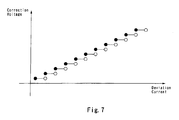
- the current difference between the measured value and the reference value is a deviation current and that the voltage of the amount for change in accordance with the correction between the power supply lines Vl to Vx and the opposing electrodes is a correction voltage
- the relationship between the deviation current and the correction voltage is illustrated in Fig. 7, for example.
- the correction voltage is changed with a constant size every time when the deviation current is changed with a constant width.
- the relationship between the deviation current and the correction voltage may not necessarily conform to the graph shown in Fig. 7. It is only necessary that the deviation current and the correction voltage have a relationship such that the value of the current actually flowing through the ammeter becomes close to the reference value.
- the relationship between the deviation current and the correction voltage may have linearity.
- the deviation current may be proportional to the second power of the correction voltage.
- the structure of the correction circuit shown in this embodiment is just one example, and the present invention is not limited to this structure. It is only necessary that the correction circuit used in the present invention has the means for measuring the measured value and the reference value and the means for performing some calculation processing based on the measured value by means of the ammeter and correcting the OLED driving voltage.
- the voltage value of the monitor variable power supply and the voltage value of the display variable power supply may not necessarily have the same structure. It may be only necessary that a calculation processing method for the time when the deviation current becomes a value equal to or larger than a certain fixed value is prescribed instead of performing correction using the current reference value stored in the memory.
- Fig. 8 shows the structure of the monitor pixel in this embodiment.
- monitor pixels 300 are provided in matrix.
- the monitor pixel 300 has a source line 301, a first gate line 302, a second gate line 303, a power supply line 304, a switching TFT 305, a driving TFT 306, an erasing TFT 309 and a monitor OLED 307.
- a gate electrode of the switching TFT 305 is connected to the first gate line 302.
- One of a source region and a drain region of the switching TFT 305 is connected to the source line 301, and the other is connected to a gate electrode of the driving TFT 306.
- a gate electrode of the erasing TFT 309 is connected to the second gate line 303.
- One of a source region and a drain region of the erasing TFT 309 is connected to the power supply line 304, and the other is connected to the gate electrode of the driving TFT 306.
- a source region of the driving TFT 306 is connected to the power supply line 304, and a drain region of the driving TFT 306 is connected to a pixel electrode of the monitor OLED 307.
- a capacitor 308 is formed between the gate electrode of the driving TFT 306 and the power supply line 304.
- the power supply line 304 is connected to a monitor variable power supply 311 through an ammeter 310. Further, opposing electrodes of the monitor OLEDs 307 are all connected to the monitor variable power supply 311. Note that, in Fig. 8, the monitor variable power supply 311 is connected such that the power supply line side is kept at a high potential (Vdd) and the opposing electrode side is kept at a low potential side (Vss). However, the present invention is not limited to this structure. It may be only necessary that the monitor variable power supply 311 is connected such that the current flowing through the monitor OLED 307 has a forward bias.
- the ammeter 310 does not necessarily provided between the monitor variable power supply 311 and the power supply line 304, and may be provided between the monitor variable power supply 311 and the opposing electrode.
- Reference numeral 312 denotes a correction circuit which controls the voltage supplied to the opposing electrode and the power supply line 304 from the monitor variable power supply 311 based on the current value (measured value) measured in the ammeter 310.
- ammeter 310 the monitor variable power supply 311 and the correction circuit 312 may be formed on the substrate different from the substrate on which the monitor pixel portion is formed, and may be connected to the monitor pixel portion through a connector or the like. If possible, the above-described components may be formed on the same substrate as the monitor pixel portion.
- a monitor variable power supply, an ammeter and a correction circuit may be provided for each color, and an OLED driving voltage may be corrected in the OLED of each color.
- the correction circuit may be provided for each color, or the common correction circuit may be provided for the OLEDs of plural colors.
- the potentials of the first gate line 302 and the second gate line 303 are controlled by different gate line driver circuits.
- the source line 301 is input with a monitor video signal by a source line driver circuit.
- the monitor video signal input to the source line 301 is input to the gate electrode of the driving TFT 306 through the switching TFT 301. Then, when the driving TFT 306 is turned on in accordance with the monitor video signal, the OLED driving voltage is applied between the pixel electrode and the opposing electrode of the monitor OLED 307 by the monitor variable power supply 311. Thus, the monitor OLED 307 emits light.
- the monitor OLED 307 does not emit light.
- the monitor OLED 307 while the monitor OLED 307 is emitting light, a current is measured in the ammeter 310. The measured value as data is sent to the correction circuit 312.
- the correction circuit 312 the measured value of the current and a fixed current value (reference value) are compared. Then, in the case where there is some difference between the measured value and the reference value, the monitor variable power supply 311 is controlled to correct the voltage between the power supply line 304 and the opposing electrode. Thus, the OLED driving voltage is corrected in the monitor OLED 307 of the monitor pixel 300, and an OLED driving current with a desired size flows.
- the OLED driving voltage may be corrected by controlling the potential at the power supply line side, or may be corrected by controlling the potential at the opposing electrode side. Also, the OLED driving voltage may be corrected by controlling both the potential at the power supply line side and the potential at the opposing electrode side.
- an image for monitor is preferably an image in which as many monitor OLEDs of the pixels as possible emit light in the pixel portion. Even if there is an error in the current value measured with the ammeter, the ratio of the error in the measured current value to the entire measured value becomes smaller as both the measured value and the reference value become larger. In the monitor image, the gradation at the same level as the average of the pixels is made in order to make the progress of deterioration uniform.
- a display pixel also has the same structure.
- the power supply line is not connected to the ammeter, and an opposing electrode of a display OLED is connected to not the monitor variable power supply but a display variable power supply.
- the structure of the pixel shown in this embodiment is just one example, and the present invention is not limited to this structure. Note that this embodiment can be implemented by freely being combined with Embodiment 1.
- the correction of the current may always be conducted, or may be conducted at the time predetermined in advance by setting. A user may arbitrarily conduct the correction of the current.
- monitor images having different reference current values may be used.
- a video signal is also input to the correction circuit, and the reference value is calculated in a calculation circuit or the like.
- the monitor image it is not necessary that a monitor video signal is used, and of course, the image to be displayed is not changed against intention of a user.
- This embodiment can be implemented by being freely combined with Embodiment 1 or 2.
- a video signal of digital (hereinafter referred to as digital video signal) of the first bit input to each of the source lines (Sl to Sx) by the source line driver circuit 105 is input to the gate electrode of the driving TFT 121 through the switching TFT 120.
- the display period Tr1 is completed, and then, a writing period Ta2 is started.
- the power supply potential of the power supply line again becomes the potential of the opposing electrode of the OLED.
- all the gate lines are selected in order, and the digital video signals of the second bit are input to all the display pixels.
- the period during which the digital video signals of the second bit are input to the display pixels of all the lines is called the writing period Ta2.
- the combination of the above display periods enables the display of a desired gradation among 2" gradations.
- both the power supply potential and the potential of the opposing electrode may always have the potential difference with an extent such that the display OLED emits light when the power supply potential is given to the pixel electrode of the display OLED.
- the display OLED can be made to emit light also in the writing periods.
- the gradation displayed by the display pixel in the frame period concerned is determined based on the total sum of the lengths of the writing periods and the display periods during which the display OLED emits light in the one frame period.
- the digital video signal which is written into and stored in the latch (B) 604 is inputted to the source signal line.
- Fig. 10B is a block figure showing the structure of gate line driving circuit.
- the timing signal from the shift resister 606 is inputted to the buffer 607, and then to a corresponding gate line.
- the gate electrodes of the TFTs for one line of pixels are connected to the gate lines, and all of the TFTs of the one line of pixels must be placed in an ON state simultaneously.
- a circuit which is capable of handling the flow of a large electric current is therefore used for the buffer.
- the p-channel TFT or the n-channel TFT manufactured by a known method is used as the driver circuit TFT 4201, and the p-channel TFT manufactured by a known method is used as the driving TFT 4202. Further, the display pixel portion 4002 is provided with a storage capacitor (not shown) connected to a gate electrode of the driving TFT 4202.
- an insulating film 4302 is formed on the pixel electrode 4203, and the insulating film 4302 is formed with an opening portion on the pixel electrode 4203.
- an organic light emitting layer 4204 is formed on the pixel electrode 4203.
- a known organic light emitting material or inorganic light emitting material may be used for the organic light emitting layer 4204. Further, there exist a low molecular weight (monomer) material and a high molecular weight (polymer) material as the organic light emitting materials, and both the materials may be used.
- a cathode 4205 made of a conductive film having light shielding property (typically, conductive film containing aluminum, copper or silver as its main constituent or lamination film of the above conductive film and another conductive film) is formed on the organic light emitting layer 4204. Further, it is desirable that moisture and oxygen that exist on an interface of the cathode 4205 and the organic light emitting layer 4204 are removed as much as possible. Therefore, such a device is necessary that the organic light emitting layer 4204 is formed in a nitrogen or rare gas atmosphere, and then, the cathode 4205 is formed without exposure to oxygen and moisture.
- the above-described film deposition is enabled by using a multi-chamber type (cluster tool type) film forming device. In addition, a predetermined voltage is given to the cathode 4205.
- a glass material, a metal material (typically, stainless material), a ceramics material or a plastic material (including a plastic film) can be used for the sealing material 4008.
- a plastic material an FRP (fiberglass-reinforced plastics) plate, a PVF (polyvinyl fluoride) film, a Mylar film, a polyester film or an acrylic resin film may be used. Further, a sheet with a structure in which an aluminum foil is sandwiched with the PVF film or the Mylar film can also be used.
- an ultraviolet curable resin or a thermosetting resin may be used as the filler 4210. so that PVC (polyvinyl chloride), acrylic, polyimide, epoxy resin, silicone resin, PVB (polyvinyl butyral) or EVA (ethylene vinyl acetate) can be used.
- nitrogen is used for the filler.
- the pixel electrode 4203 is formed, and at the same time, a conductive film 4203a is formed so as to contact the drawn wiring 4005a.
- anisotropic conductive film 4300 has conductive filler 4300a.
- the conductive film 4203a on the substrate 4001 and the FPC wiring 4301 on the FPC 4006 are electrically connected to each other by the conductive filler 4300a by heat-pressing the substrate 4001 and the FPC 4006.
- the light emitted from the monitor pixel portion may penetrate the substrate 4001 or the cover member 4208 or not.
- the image displayed in the monitor pixel portion can be effectively utilized for displaying something.
- the ammeter, the variable power supply and the correction circuit of the light emitting device of the present invention are formed on a substrate (not shown) different from the substrate 4001, and are electrically connected to the power supply line and the cathode 4205, which are formed on the substrate 4001, through the FPC 4006.
- the ammeter, the variable power supply and the correction circuit of the light emitting device of the present invention are formed on a substrate different from the substrate on which the display pixel portion is formed, and are connected to the wirings on the substrate on which the display pixel portion is formed by a means such as a wire bonding method or a COG (chip-on-glass) method.
- Fig. 12 is a diagram of an appearance of a light emitting device of this embodiment.
- a seal member 5009 is provided so as to surround a display pixel portion 5002, a monitor pixel portion 5070, a source line driver circuit 5003 and a gate line driver circuit 5004 which are provided on a substrate 5001. Further, a sealing material 5008 is provided on the display pixel portion 5002, the monitor pixel portion 5070, the source line driver circuit 5003 and the gate line driver circuit 5004.
- the display pixel portion 5002, the monitor pixel portion 5070, the source line driver circuit 5003 and the gate line driver circuit 5004 are sealed by the substrate 5001, the seal member 5009 and the sealing member 5008 together with a filler (not shown).
- a concave portion 5007 is provided on the surface of the sealing material 5008 on the substrate 5001 side, and a hygroscopic substance or a substance that can absorb oxygen is arranged therein.
- the chip 5020 on which the ammeter, the variable power supply and the correction circuit are formed is attached onto the substrate 5001 by the wire bonding method, the COG method or the like.
- the light emitting device can be structured based on one substrate, and therefore, the device itself is made compact and also the mechanical strength is improved.
- circuits and elements other than the ammeter, the variable power supply and the correction circuit may be attached onto the substrate 5001.
- This embodiment can be implemented by being freely combined with Embodiments 1 to 6.
- an external light emitting quantum efficiency can be remarkably improved by using an organic material by which phosphorescence from a triplet exciton can be employed for emitting a light.
- the power consumption of the OLED can be reduced, the lifetime of the OLED can be elongated and the weight of the OLED can be lightened.
- This embodiment uses a substrate 900 of a glass such as barium borosilicate glass or aluminoborosilicate glass as represented by the glass #7059 or the glass #1737 of Corning Co.
- a substrate 900 of a glass such as barium borosilicate glass or aluminoborosilicate glass as represented by the glass #7059 or the glass #1737 of Corning Co.
- the substrate 900 has a property of transmitting light, and there may be used a quartz substrate.
- a plastic substrate having heat resistance capable of withstanding the treatment temperature of this embodiment.
- the Ta film that is used as the heat-resistant conductive layer 907 can similarly be formed by the sputtering method.
- the Ta film is formed by using Ar as a sputtering gas. Further, the addition of suitable amounts of Xe and Kr into the gas during the sputtering makes it possible to relax the internal stress of the film that is formed and to prevent the film from being peeled off.
- the Ta film of ⁇ -phase has a resistivity of about 20 ⁇ cm and can be used as the gate electrode but the Ta film of ⁇ -phase has a resistivity of about 180 ⁇ cm and is not suited for use as the gate electrode.
- the TaN film has a crystalline structure close to the ⁇ -phase.
- the conductive layers 909 to 912 having a first tapered shape are formed by the first etching treatment.
- the conductive layers 909 to 912 are tapered at an angle of from 15 to 30°.
- over-etching is conducted by increasing the etching time by about 10 to 20%.
- the selection ratio of the silicon oxynitride film (gate insulating film 906) to the W film is 2 to 4 (typically, 3). Due to the over etching, therefore, the surface where the silicon oxynitride film is exposed is etched by about 20 to about 50 nm (Fig. 13(B)).
- the dosage is set to be from 1 x 10 13 to 5 x 10 14 atoms/cm 2 so that the impurity element for imparting the n-type reaches the underlying semiconductor layer penetrating through the tapered portion and the gate insulating film 906 at the ends of the gate electrode, and the acceleration voltage is selected to be from 80 to 160 keV.
- the impurity element for imparting the n-type there is used an element belonging to the Group 15 and, typically, phosphorus (P) or arsenic (As). Phosphorus (P) is used, here.
- a first interlayer insulating film 937 is formed on the conductive layers 918 to 921 of the second shape and on the gate insulating film 906.
- the first interlayer insulating film 937 may be formed of a silicon oxide film, a silicon oxynitride film, a silicon nitride film, or a laminated layer film of a combination thereof.
- the first interlayer insulating film 937 is formed of an inorganic insulating material.
- the first interlayer insulating film 937 has a thickness of 100 to 200 nm.
- the atmospheric gas is changed, and the heat treatment is conducted in an atmosphere containing 3 to 100% of hydrogen at from 300 to 450°C for from 1 to 12 hours to hydrogenate the semiconductor layer.
- This step is to terminate the dangling bonds of 10 16 to 10 18 /cm 3 in the semiconductor layer with hydrogen that is thermally excited.
- the plasma hydrogenation may be executed (using hydrogen excited with plasma). In any way, it is desired that the defect density in the semiconductor layers 902 to 905 is suppressed to be not larger than 10 16 /cm 3 .
- hydrogen may be added in an amount of from 0.01 to 0.1 atomic %.
- the driving circuit can be operated by a power supply having a voltage of 5 to 6V, 10 V, at most. Therefore, degradation of TFTs due to hot electron is not a serious problem. Also, smaller gate capacitance is preferred for the TFTs since the driving circuit needs to operate at high speed. Accordingly, in a driving circuit of a light emitting device using OLED as in this embodiment, the second impurity region 929 and the fourth impurity region 933b of the semiconductor layers of the TFTs preferably do not overlap the gate electrode 918 and the gate electrode 919, respectively.
- the pixel electrode 947 is formed so as to contact and overlap the drain wiring 946. Thus, electrical connection between the pixel electrode 947 and the drain region of the driving TFT is formed.
- the third interlayer insulating film 982 having an opening portion at the position corresponding to the pixel electrode 947 is formed.
- side walls having a tapered shape are formed by using a wet etching method in forming the opening portion.
- the organic light emitting layer formed on the third interlayer insulating film 982 is not separated.
- the deterioration of the organic light emitting layer which derives from a step becomes a conspicuous problem if the side walls of the opening portion are not sufficiently gentle, which requires attention.
- Fig. 17G illustrates a video camera which includes a main body 2601, a display portion 2602, a casing 2603, an external connecting port 2604, a remote control receiving portion 2605, an image receiving portion 2606, a battery 2607, a sound input portion 2608, an operation key 2609, or the like.
- the light emitting device in accordance with the present invention can be used as the display portion 2602.
Landscapes
- Engineering & Computer Science (AREA)
- Physics & Mathematics (AREA)
- Computer Hardware Design (AREA)
- General Physics & Mathematics (AREA)
- Theoretical Computer Science (AREA)
- Electroluminescent Light Sources (AREA)
- Control Of Indicators Other Than Cathode Ray Tubes (AREA)
- Control Of El Displays (AREA)
Applications Claiming Priority (2)
| Application Number | Priority Date | Filing Date | Title |
|---|---|---|---|
| JP2001019651 | 2001-01-29 | ||
| JP2001019651 | 2001-01-29 |
Publications (3)
| Publication Number | Publication Date |
|---|---|
| EP1227467A2 true EP1227467A2 (fr) | 2002-07-31 |
| EP1227467A3 EP1227467A3 (fr) | 2003-04-23 |
| EP1227467B1 EP1227467B1 (fr) | 2006-11-15 |
Family
ID=18885494
Family Applications (1)
| Application Number | Title | Priority Date | Filing Date |
|---|---|---|---|
| EP02001895A Expired - Lifetime EP1227467B1 (fr) | 2001-01-29 | 2002-01-28 | Dispositif d'émission de lumière avec réglage du courant |
Country Status (8)
| Country | Link |
|---|---|
| US (2) | US6788003B2 (fr) |
| EP (1) | EP1227467B1 (fr) |
| KR (1) | KR100843989B1 (fr) |
| CN (2) | CN100449768C (fr) |
| DE (1) | DE60215983T2 (fr) |
| MY (1) | MY127343A (fr) |
| SG (1) | SG111928A1 (fr) |
| TW (1) | TW569016B (fr) |
Cited By (17)
| Publication number | Priority date | Publication date | Assignee | Title |
|---|---|---|---|---|
| EP1318499A3 (fr) * | 2001-11-27 | 2003-08-27 | Pioneer Corporation | Dispositif d'affichage à panneau d'affichage à matrice active |
| GB2389952A (en) * | 2002-06-18 | 2003-12-24 | Cambridge Display Tech Ltd | Driver circuits for electroluminescent displays with reduced power consumption |
| WO2004021327A1 (fr) * | 2002-08-27 | 2004-03-11 | E.I. Du Pont De Nemours And Company | Afficheur electronique couleurs a lignes d'alimentation electrique separees |
| US6710548B2 (en) | 2001-02-08 | 2004-03-23 | Semiconductor Energy Laboratory Co., Ltd. | Light emitting device and electronic equipment using the same |
| WO2004040541A1 (fr) | 2002-10-31 | 2004-05-13 | Semiconductor Energy Laboratory Co., Ltd. | Dispositif d'affichage et son procede de commande |
| WO2004088626A1 (fr) * | 2003-04-01 | 2004-10-14 | Koninklijke Philips Electronics N.V. | Dispositif d’affichage a matrice active comportant un circuit de modelisation situe a l’exterieur de la zone d’affichage pour compenser les variations de seuil du transistor d’attaque des pixels |
| GB2400691A (en) * | 2003-04-16 | 2004-10-20 | Peter Norman Langmead | Controlling voltage supply for current dependent electronic devices |
| US7042427B2 (en) | 2001-01-29 | 2006-05-09 | Semiconductor Energy Laboratory Co., Ltd. | Light emitting device |
| US7081704B2 (en) | 2002-08-09 | 2006-07-25 | Semiconductor Energy Laboratory Co., Ltd. | Semiconductor device and manufacturing method thereof |
| EP1768093A3 (fr) * | 2005-09-27 | 2008-04-02 | LG Electronics Inc. | Dispositif électroluminescent et son procédé de commande |
| US7598935B2 (en) | 2005-05-17 | 2009-10-06 | Lg Electronics Inc. | Light emitting device with cross-talk preventing circuit and method of driving the same |
| EP2023326A3 (fr) * | 2007-07-27 | 2010-03-10 | Samsung Mobile Display Co., Ltd. | Affichage électroluminescent organique et son procédé de commande |
| US7924041B2 (en) * | 2008-02-14 | 2011-04-12 | Samsung Electronics Co., Ltd. | Liquid crystal display including sensing unit for compensation driving |
| US8111215B2 (en) | 2004-05-22 | 2012-02-07 | Semiconductor Energy Laboratory Co., Ltd. | Display device and electronic device |
| US8154189B2 (en) | 2006-01-07 | 2012-04-10 | Semiconductor Energy Laboratory Co., Ltd. | Display device and manufacturing method of the same |
| US8194006B2 (en) | 2004-08-23 | 2012-06-05 | Semiconductor Energy Laboratory Co., Ltd. | Display device, driving method of the same, and electronic device comprising monitoring elements |
| US9305491B2 (en) | 2006-06-30 | 2016-04-05 | Sébastien Weitbruch | Method and apparatus for driving a display device with variable reference driving signals |
Families Citing this family (146)
| Publication number | Priority date | Publication date | Assignee | Title |
|---|---|---|---|---|
| US6828950B2 (en) * | 2000-08-10 | 2004-12-07 | Semiconductor Energy Laboratory Co., Ltd. | Display device and method of driving the same |
| SG111928A1 (en) * | 2001-01-29 | 2005-06-29 | Semiconductor Energy Lab | Light emitting device |
| JP2003195810A (ja) * | 2001-12-28 | 2003-07-09 | Casio Comput Co Ltd | 駆動回路、駆動装置及び光学要素の駆動方法 |
| US6806497B2 (en) * | 2002-03-29 | 2004-10-19 | Seiko Epson Corporation | Electronic device, method for driving the electronic device, electro-optical device, and electronic equipment |
| EP2249413A3 (fr) * | 2002-04-01 | 2011-02-02 | Konica Corporation | Support et élément électroluminescent organique comprenant ce support |
| JP3918642B2 (ja) * | 2002-06-07 | 2007-05-23 | カシオ計算機株式会社 | 表示装置及びその駆動方法 |
| JP4610843B2 (ja) | 2002-06-20 | 2011-01-12 | カシオ計算機株式会社 | 表示装置及び表示装置の駆動方法 |
| JP4115763B2 (ja) * | 2002-07-10 | 2008-07-09 | パイオニア株式会社 | 表示装置及び表示方法 |
| JP4103500B2 (ja) * | 2002-08-26 | 2008-06-18 | カシオ計算機株式会社 | 表示装置及び表示パネルの駆動方法 |
| US20040075628A1 (en) * | 2002-10-21 | 2004-04-22 | Chih-Chung Chien | Double-side display device |
| TWI290008B (en) * | 2002-12-24 | 2007-11-11 | Ritdisplay Corp | Active driven organic electroluminescent device |
| US7161566B2 (en) * | 2003-01-31 | 2007-01-09 | Eastman Kodak Company | OLED display with aging compensation |
| JP4571375B2 (ja) * | 2003-02-19 | 2010-10-27 | 東北パイオニア株式会社 | アクティブ駆動型発光表示装置およびその駆動制御方法 |
| JP3952965B2 (ja) * | 2003-02-25 | 2007-08-01 | カシオ計算機株式会社 | 表示装置及び表示装置の駆動方法 |
| CN1317688C (zh) * | 2003-03-13 | 2007-05-23 | 统宝光电股份有限公司 | 数据驱动装置 |
| CN1329880C (zh) * | 2003-03-21 | 2007-08-01 | 友达光电股份有限公司 | 可自动调节阴极电压的有源矩阵有机发光二极管电路及其自动调节方法 |
| JP3912313B2 (ja) * | 2003-03-31 | 2007-05-09 | セイコーエプソン株式会社 | 画素回路、電気光学装置および電子機器 |
| CN1312650C (zh) * | 2003-04-03 | 2007-04-25 | 胜华科技股份有限公司 | 主动式有机发光二极管显示器影像均匀的方法及装置 |
| US7580033B2 (en) * | 2003-07-16 | 2009-08-25 | Honeywood Technologies, Llc | Spatial-based power savings |
| US20060020906A1 (en) * | 2003-07-16 | 2006-01-26 | Plut William J | Graphics preservation for spatially varying display device power conversation |
| US7714831B2 (en) * | 2003-07-16 | 2010-05-11 | Honeywood Technologies, Llc | Background plateau manipulation for display device power conservation |
| US7602388B2 (en) * | 2003-07-16 | 2009-10-13 | Honeywood Technologies, Llc | Edge preservation for spatially varying power conservation |
| US7663597B2 (en) | 2003-07-16 | 2010-02-16 | Honeywood Technologies, Llc | LCD plateau power conservation |
| US7786988B2 (en) | 2003-07-16 | 2010-08-31 | Honeywood Technologies, Llc | Window information preservation for spatially varying power conservation |
| US7583260B2 (en) * | 2003-07-16 | 2009-09-01 | Honeywood Technologies, Llc | Color preservation for spatially varying power conservation |
| JP5021884B2 (ja) | 2003-08-06 | 2012-09-12 | 日本電気株式会社 | 表示駆動回路及びそれを用いた表示装置 |
| JP2005099713A (ja) * | 2003-08-25 | 2005-04-14 | Seiko Epson Corp | 電気光学装置、電気光学装置の駆動方法及び電子機器 |
| JP4534052B2 (ja) * | 2003-08-27 | 2010-09-01 | 奇美電子股▲ふん▼有限公司 | 有機el基板の検査方法 |
| CA2443206A1 (fr) | 2003-09-23 | 2005-03-23 | Ignis Innovation Inc. | Panneaux arriere d'ecran amoled - circuits de commande des pixels, architecture de reseau et compensation externe |
| JP2005107059A (ja) * | 2003-09-29 | 2005-04-21 | Sanyo Electric Co Ltd | 表示装置 |
| US8264431B2 (en) | 2003-10-23 | 2012-09-11 | Massachusetts Institute Of Technology | LED array with photodetector |
| JP4804711B2 (ja) * | 2003-11-21 | 2011-11-02 | 株式会社 日立ディスプレイズ | 画像表示装置 |
| JP2005157202A (ja) * | 2003-11-28 | 2005-06-16 | Tohoku Pioneer Corp | 自発光表示装置 |
| JP4203656B2 (ja) * | 2004-01-16 | 2009-01-07 | カシオ計算機株式会社 | 表示装置及び表示パネルの駆動方法 |
| KR100989708B1 (ko) * | 2004-01-26 | 2010-10-26 | 엘지전자 주식회사 | 이동 통신 단말기의 이중 디스플레이 패널 제어 장치 |
| JP4665419B2 (ja) * | 2004-03-30 | 2011-04-06 | カシオ計算機株式会社 | 画素回路基板の検査方法及び検査装置 |
| JP4239890B2 (ja) * | 2004-04-26 | 2009-03-18 | セイコーエプソン株式会社 | 有機el装置、電子機器 |
| US20050249699A1 (en) * | 2004-05-05 | 2005-11-10 | Stoff Jesse A | Immunodynamic complexes and methods for using and preparing such complexes |
| JP4026618B2 (ja) * | 2004-05-20 | 2007-12-26 | セイコーエプソン株式会社 | 電気光学装置、その検査方法および電子機器 |
| CA2472671A1 (fr) | 2004-06-29 | 2005-12-29 | Ignis Innovation Inc. | Procede de programmation par tensions pour affichages a del excitees par courant |
| KR101246642B1 (ko) * | 2004-07-23 | 2013-03-25 | 가부시키가이샤 한도오따이 에네루기 켄큐쇼 | 표시 장치 및 이의 구동 방법 |
| WO2006011666A1 (fr) * | 2004-07-30 | 2006-02-02 | Semiconductor Energy Laboratory Co., Ltd. | Dispositif d’affichage, procede d’entrainement de celui-ci et appareil electronique |
| KR100698689B1 (ko) * | 2004-08-30 | 2007-03-23 | 삼성에스디아이 주식회사 | 발광 표시장치와 그의 제조방법 |
| JP4437110B2 (ja) * | 2004-11-17 | 2010-03-24 | 三星モバイルディスプレイ株式會社 | 有機発光表示装置,有機発光表示装置の駆動方法及び画素回路の駆動方法 |
| US10012678B2 (en) | 2004-12-15 | 2018-07-03 | Ignis Innovation Inc. | Method and system for programming, calibrating and/or compensating, and driving an LED display |
| US8599191B2 (en) | 2011-05-20 | 2013-12-03 | Ignis Innovation Inc. | System and methods for extraction of threshold and mobility parameters in AMOLED displays |
| TWI402790B (zh) | 2004-12-15 | 2013-07-21 | Ignis Innovation Inc | 用以程式化,校準及驅動一發光元件顯示器的方法及系統 |
| US10013907B2 (en) | 2004-12-15 | 2018-07-03 | Ignis Innovation Inc. | Method and system for programming, calibrating and/or compensating, and driving an LED display |
| US9799246B2 (en) | 2011-05-20 | 2017-10-24 | Ignis Innovation Inc. | System and methods for extraction of threshold and mobility parameters in AMOLED displays |
| US20140111567A1 (en) | 2005-04-12 | 2014-04-24 | Ignis Innovation Inc. | System and method for compensation of non-uniformities in light emitting device displays |
| US9280933B2 (en) | 2004-12-15 | 2016-03-08 | Ignis Innovation Inc. | System and methods for extraction of threshold and mobility parameters in AMOLED displays |
| US8576217B2 (en) | 2011-05-20 | 2013-11-05 | Ignis Innovation Inc. | System and methods for extraction of threshold and mobility parameters in AMOLED displays |
| US9171500B2 (en) | 2011-05-20 | 2015-10-27 | Ignis Innovation Inc. | System and methods for extraction of parasitic parameters in AMOLED displays |
| US9275579B2 (en) | 2004-12-15 | 2016-03-01 | Ignis Innovation Inc. | System and methods for extraction of threshold and mobility parameters in AMOLED displays |
| US20060132400A1 (en) * | 2004-12-20 | 2006-06-22 | Eastman Kodak Company | Ambient light detection using an OLED device |
| US8405579B2 (en) | 2004-12-24 | 2013-03-26 | Samsung Display Co., Ltd. | Data driver and light emitting diode display device including the same |
| KR100624318B1 (ko) * | 2004-12-24 | 2006-09-19 | 삼성에스디아이 주식회사 | 데이터 집적회로 및 이를 이용한 발광 표시장치와 그의구동방법 |
| KR100611914B1 (ko) | 2004-12-24 | 2006-08-11 | 삼성에스디아이 주식회사 | 데이터 집적회로 및 이를 이용한 발광 표시장치와 그의구동방법 |
| KR100613093B1 (ko) * | 2004-12-24 | 2006-08-16 | 삼성에스디아이 주식회사 | 데이터 집적회로 및 이를 이용한 발광 표시장치 |
| US7646367B2 (en) | 2005-01-21 | 2010-01-12 | Semiconductor Energy Laboratory Co., Ltd. | Semiconductor device, display device and electronic apparatus |
| CA2496642A1 (fr) | 2005-02-10 | 2006-08-10 | Ignis Innovation Inc. | Methode d'attaque a courte duree de stabilisation pour afficheurs a diodes organiques electroluminescentes (oled) programmes par courant |
| US8681077B2 (en) * | 2005-03-18 | 2014-03-25 | Semiconductor Energy Laboratory Co., Ltd. | Semiconductor device, and display device, driving method and electronic apparatus thereof |
| KR100712288B1 (ko) * | 2005-03-22 | 2007-04-27 | 삼성에스디아이 주식회사 | 화면 일부에 저휘도 화소들로 이루어진 이미지를 구비하는평판표시장치 및 그의 제조방법 |
| EP1729280B1 (fr) * | 2005-03-31 | 2013-10-30 | Semiconductor Energy Laboratory Co., Ltd. | Dispositif d'affichage, module d'affichage, appareil électronique et procédé de commande du dispositif d'affichage |
| CN100538794C (zh) * | 2005-05-02 | 2009-09-09 | 株式会社半导体能源研究所 | 发光器件及其驱动方法、显示模块以及电子器具 |
| US7760210B2 (en) * | 2005-05-04 | 2010-07-20 | Honeywood Technologies, Llc | White-based power savings |
| US7602408B2 (en) | 2005-05-04 | 2009-10-13 | Honeywood Technologies, Llc | Luminance suppression power conservation |
| CN102663977B (zh) | 2005-06-08 | 2015-11-18 | 伊格尼斯创新有限公司 | 用于驱动发光器件显示器的方法和系统 |
| JP5020484B2 (ja) * | 2005-07-12 | 2012-09-05 | 東北パイオニア株式会社 | 自発光表示装置及びその駆動方法 |
| TW200705083A (en) * | 2005-07-29 | 2007-02-01 | Coretronic Corp | Projector |
| CA2518276A1 (fr) | 2005-09-13 | 2007-03-13 | Ignis Innovation Inc. | Technique de compensation de la degradation de luminance dans des dispositifs electroluminescents |
| KR100708715B1 (ko) * | 2005-09-30 | 2007-04-17 | 삼성에스디아이 주식회사 | 유기 발광 디스플레이 장치 |
| US7995012B2 (en) * | 2005-12-27 | 2011-08-09 | Semiconductor Energy Laboratory Co., Ltd. | Light emitting device |
| EP1804229B1 (fr) * | 2005-12-28 | 2016-08-17 | Semiconductor Energy Laboratory Co., Ltd. | Dispositif d'affichage et son procédé d'inspection |
| KR101240648B1 (ko) | 2006-01-10 | 2013-03-08 | 삼성디스플레이 주식회사 | 유기 발광 표시 장치 및 그 제조 방법 |
| JP4360375B2 (ja) * | 2006-03-20 | 2009-11-11 | セイコーエプソン株式会社 | 電気光学装置、電子機器、及び駆動方法 |
| CN101501748B (zh) | 2006-04-19 | 2012-12-05 | 伊格尼斯创新有限公司 | 有源矩阵显示器的稳定驱动设计 |
| US20070290947A1 (en) * | 2006-06-16 | 2007-12-20 | Cok Ronald S | Method and apparatus for compensating aging of an electroluminescent display |
| US20070290958A1 (en) * | 2006-06-16 | 2007-12-20 | Eastman Kodak Company | Method and apparatus for averaged luminance and uniformity correction in an amoled display |
| US7696965B2 (en) * | 2006-06-16 | 2010-04-13 | Global Oled Technology Llc | Method and apparatus for compensating aging of OLED display |
| US20080042943A1 (en) * | 2006-06-16 | 2008-02-21 | Cok Ronald S | Method and apparatus for averaged luminance and uniformity correction in an am-el display |
| KR20080010796A (ko) * | 2006-07-28 | 2008-01-31 | 삼성전자주식회사 | 유기 발광 표시 장치 및 그의 구동 방법 |
| CA2556961A1 (fr) | 2006-08-15 | 2008-02-15 | Ignis Innovation Inc. | Technique de compensation de diodes electroluminescentes organiques basee sur leur capacite |
| JP2008134577A (ja) * | 2006-10-24 | 2008-06-12 | Eastman Kodak Co | 表示装置及びその製造方法 |
| KR100826011B1 (ko) | 2006-10-24 | 2008-04-29 | 엘지디스플레이 주식회사 | 디스플레이 소자 |
| US8988328B2 (en) * | 2006-11-30 | 2015-03-24 | Sharp Kabushiki Kaisha | Display device configured to supply a driving current in accordance with a signal voltage selected based on a temperature dependency of the driving current and driving method thereof |
| US8188942B2 (en) * | 2007-03-08 | 2012-05-29 | Lg Electronics Inc. | Light emitting device |
| KR100870523B1 (ko) * | 2007-03-21 | 2008-11-26 | 엘지디스플레이 주식회사 | 전계발광표시장치와 그 구동방법 |
| KR100903476B1 (ko) * | 2007-04-24 | 2009-06-18 | 삼성모바일디스플레이주식회사 | 유기 전계 발광 표시 장치 및 그 구동 방법 |
| KR100896046B1 (ko) * | 2007-07-24 | 2009-05-11 | 엘지전자 주식회사 | 유기전계발광표시장치 |
| KR101281681B1 (ko) * | 2007-11-06 | 2013-07-03 | 삼성디스플레이 주식회사 | 휘도 변화를 보상하기 위한 구동 전압 조정 장치 및 구동전압 조정 방법 |
| KR100902219B1 (ko) * | 2007-12-05 | 2009-06-11 | 삼성모바일디스플레이주식회사 | 유기전계발광 표시장치 |
| KR101017164B1 (ko) * | 2008-03-27 | 2011-02-25 | 가부시키가이샤 히타치 디스프레이즈 | 화상 표시 장치 |
| US8217928B2 (en) * | 2009-03-03 | 2012-07-10 | Global Oled Technology Llc | Electroluminescent subpixel compensated drive signal |
| CN102356697B (zh) * | 2009-03-18 | 2014-05-28 | 株式会社半导体能源研究所 | 照明装置 |
| JP2010243736A (ja) * | 2009-04-03 | 2010-10-28 | Sony Corp | 表示装置 |
| US9384698B2 (en) | 2009-11-30 | 2016-07-05 | Ignis Innovation Inc. | System and methods for aging compensation in AMOLED displays |
| US9311859B2 (en) | 2009-11-30 | 2016-04-12 | Ignis Innovation Inc. | Resetting cycle for aging compensation in AMOLED displays |
| CA2669367A1 (fr) | 2009-06-16 | 2010-12-16 | Ignis Innovation Inc | Technique de compensation pour la variation chromatique des ecrans d'affichage . |
| US10319307B2 (en) | 2009-06-16 | 2019-06-11 | Ignis Innovation Inc. | Display system with compensation techniques and/or shared level resources |
| CA2688870A1 (fr) | 2009-11-30 | 2011-05-30 | Ignis Innovation Inc. | Procede et techniques pour ameliorer l'uniformite d'affichage |
| US10996258B2 (en) | 2009-11-30 | 2021-05-04 | Ignis Innovation Inc. | Defect detection and correction of pixel circuits for AMOLED displays |
| US8803417B2 (en) | 2009-12-01 | 2014-08-12 | Ignis Innovation Inc. | High resolution pixel architecture |
| CA2687631A1 (fr) | 2009-12-06 | 2011-06-06 | Ignis Innovation Inc | Mecanisme de commande a faible puissance pour applications d'affichage |
| US10163401B2 (en) | 2010-02-04 | 2018-12-25 | Ignis Innovation Inc. | System and methods for extracting correlation curves for an organic light emitting device |
| US10176736B2 (en) | 2010-02-04 | 2019-01-08 | Ignis Innovation Inc. | System and methods for extracting correlation curves for an organic light emitting device |
| US9881532B2 (en) | 2010-02-04 | 2018-01-30 | Ignis Innovation Inc. | System and method for extracting correlation curves for an organic light emitting device |
| US20140313111A1 (en) | 2010-02-04 | 2014-10-23 | Ignis Innovation Inc. | System and methods for extracting correlation curves for an organic light emitting device |
| CA2692097A1 (fr) | 2010-02-04 | 2011-08-04 | Ignis Innovation Inc. | Extraction de courbes de correlation pour des dispositifs luminescents |
| US10089921B2 (en) | 2010-02-04 | 2018-10-02 | Ignis Innovation Inc. | System and methods for extracting correlation curves for an organic light emitting device |
| CA2696778A1 (fr) | 2010-03-17 | 2011-09-17 | Ignis Innovation Inc. | Procedes d'extraction des parametres d'uniformite de duree de vie |
| KR20120022411A (ko) | 2010-09-02 | 2012-03-12 | 삼성모바일디스플레이주식회사 | 표시 장치 및 그 구동 방법 |
| KR101824125B1 (ko) * | 2010-09-10 | 2018-02-01 | 가부시키가이샤 한도오따이 에네루기 켄큐쇼 | 표시 장치 |
| US8907991B2 (en) | 2010-12-02 | 2014-12-09 | Ignis Innovation Inc. | System and methods for thermal compensation in AMOLED displays |
| US9530349B2 (en) | 2011-05-20 | 2016-12-27 | Ignis Innovations Inc. | Charged-based compensation and parameter extraction in AMOLED displays |
| US9466240B2 (en) | 2011-05-26 | 2016-10-11 | Ignis Innovation Inc. | Adaptive feedback system for compensating for aging pixel areas with enhanced estimation speed |
| US9773439B2 (en) | 2011-05-27 | 2017-09-26 | Ignis Innovation Inc. | Systems and methods for aging compensation in AMOLED displays |
| US8405086B1 (en) * | 2011-11-04 | 2013-03-26 | Shenzhen China Star Optoelectronics Technology Co., Ltd. | Pixel structure of display panel and method for manufacturing the same |
| US9324268B2 (en) | 2013-03-15 | 2016-04-26 | Ignis Innovation Inc. | Amoled displays with multiple readout circuits |
| US10089924B2 (en) | 2011-11-29 | 2018-10-02 | Ignis Innovation Inc. | Structural and low-frequency non-uniformity compensation |
| US8937632B2 (en) | 2012-02-03 | 2015-01-20 | Ignis Innovation Inc. | Driving system for active-matrix displays |
| US9747834B2 (en) | 2012-05-11 | 2017-08-29 | Ignis Innovation Inc. | Pixel circuits including feedback capacitors and reset capacitors, and display systems therefore |
| US8922544B2 (en) | 2012-05-23 | 2014-12-30 | Ignis Innovation Inc. | Display systems with compensation for line propagation delay |
| KR101922002B1 (ko) * | 2012-06-22 | 2019-02-21 | 삼성디스플레이 주식회사 | 유기 전계 표시 장치 |
| US9786223B2 (en) | 2012-12-11 | 2017-10-10 | Ignis Innovation Inc. | Pixel circuits for AMOLED displays |
| US9336717B2 (en) | 2012-12-11 | 2016-05-10 | Ignis Innovation Inc. | Pixel circuits for AMOLED displays |
| US9171504B2 (en) | 2013-01-14 | 2015-10-27 | Ignis Innovation Inc. | Driving scheme for emissive displays providing compensation for driving transistor variations |
| US9830857B2 (en) | 2013-01-14 | 2017-11-28 | Ignis Innovation Inc. | Cleaning common unwanted signals from pixel measurements in emissive displays |
| EP3043338A1 (fr) | 2013-03-14 | 2016-07-13 | Ignis Innovation Inc. | Re-interpolation avec détection de bord pour extraire un motif de vieillissement d'écrans amoled |
| CN105144361B (zh) | 2013-04-22 | 2019-09-27 | 伊格尼斯创新公司 | 用于oled显示面板的检测系统 |
| DE112014003719T5 (de) | 2013-08-12 | 2016-05-19 | Ignis Innovation Inc. | Kompensationsgenauigkeit |
| US9741282B2 (en) | 2013-12-06 | 2017-08-22 | Ignis Innovation Inc. | OLED display system and method |
| US9761170B2 (en) | 2013-12-06 | 2017-09-12 | Ignis Innovation Inc. | Correction for localized phenomena in an image array |
| US9502653B2 (en) | 2013-12-25 | 2016-11-22 | Ignis Innovation Inc. | Electrode contacts |
| CN103681772B (zh) * | 2013-12-27 | 2018-09-11 | 京东方科技集团股份有限公司 | 一种阵列基板和显示装置 |
| DE102015206281A1 (de) | 2014-04-08 | 2015-10-08 | Ignis Innovation Inc. | Anzeigesystem mit gemeinsam genutzten Niveauressourcen für tragbare Vorrichtungen |
| KR20150142943A (ko) * | 2014-06-12 | 2015-12-23 | 삼성디스플레이 주식회사 | 유기 발광 표시 장치 |
| CN104361859B (zh) * | 2014-11-18 | 2017-01-11 | 深圳市华星光电技术有限公司 | 显示装置及其亮度调节方法 |
| US9728125B2 (en) * | 2014-12-22 | 2017-08-08 | Shenzhen China Star Optoelectronics Technology Co., Ltd | AMOLED pixel circuit |
| CA2879462A1 (fr) | 2015-01-23 | 2016-07-23 | Ignis Innovation Inc. | Compensation de la variation de couleur dans les dispositifs emetteurs |
| CA2889870A1 (fr) | 2015-05-04 | 2016-11-04 | Ignis Innovation Inc. | Systeme de retroaction optique |
| CA2892714A1 (fr) | 2015-05-27 | 2016-11-27 | Ignis Innovation Inc | Reduction de largeur de bande de memoire dans un systeme de compensation |
| CA2900170A1 (fr) | 2015-08-07 | 2017-02-07 | Gholamreza Chaji | Etalonnage de pixel fonde sur des valeurs de reference ameliorees |
| CN109388273B (zh) * | 2017-08-14 | 2020-10-30 | 京东方科技集团股份有限公司 | 触控显示面板及其驱动方法、电子装置 |
| TWI711027B (zh) * | 2019-12-04 | 2020-11-21 | 友達光電股份有限公司 | 畫素補償電路與顯示裝置 |
| CN114927550B (zh) * | 2022-05-26 | 2023-06-09 | 惠科股份有限公司 | 显示面板和显示装置 |
Family Cites Families (15)
| Publication number | Priority date | Publication date | Assignee | Title |
|---|---|---|---|---|
| GB2106299B (en) * | 1981-09-23 | 1985-06-19 | Smiths Industries Plc | Electroluminescent display devices |
| JPH09115673A (ja) * | 1995-10-13 | 1997-05-02 | Sony Corp | 発光素子又は装置、及びその駆動方法 |
| JP3309738B2 (ja) * | 1996-11-01 | 2002-07-29 | 松下電器産業株式会社 | 画像表示装置 |
| TW352415B (en) * | 1996-12-26 | 1999-02-11 | Fuji Photo Film Co Ltd | Still camera |
| KR100550020B1 (ko) * | 1997-03-12 | 2006-10-31 | 세이코 엡슨 가부시키가이샤 | 전류구동형발광소자를구비한화소회로,표시장치및전자기기 |
| DE69825402T2 (de) * | 1997-03-12 | 2005-08-04 | Seiko Epson Corp. | Pixelschaltung, anzeigevorrichtung und elektronische apparatur mit stromgesteuerter lichtemittierender vorrichtung |
| JP3394187B2 (ja) * | 1997-08-08 | 2003-04-07 | シャープ株式会社 | 座標入力装置および表示一体型座標入力装置 |
| JP3767877B2 (ja) * | 1997-09-29 | 2006-04-19 | 三菱化学株式会社 | アクティブマトリックス発光ダイオード画素構造およびその方法 |
| DE69936008T2 (de) * | 1998-01-07 | 2008-01-10 | Tdk Corp. | Keramischer Kondensator |
| JP2000200067A (ja) * | 1998-11-06 | 2000-07-18 | Matsushita Electric Ind Co Ltd | 表示装置の駆動方法及び表示装置 |
| JP2000214825A (ja) * | 1999-01-20 | 2000-08-04 | Nec Corp | バックライト表示装置及び方法 |
| JP5210473B2 (ja) * | 1999-06-21 | 2013-06-12 | 株式会社半導体エネルギー研究所 | 表示装置 |
| TW480727B (en) * | 2000-01-11 | 2002-03-21 | Semiconductor Energy Laboratro | Semiconductor display device |
| JP2001223074A (ja) * | 2000-02-07 | 2001-08-17 | Futaba Corp | 有機エレクトロルミネッセンス素子及びその駆動方法 |
| SG111928A1 (en) * | 2001-01-29 | 2005-06-29 | Semiconductor Energy Lab | Light emitting device |
-
2002
- 2002-01-23 SG SG200200366A patent/SG111928A1/en unknown
- 2002-01-23 TW TW091101090A patent/TW569016B/zh not_active IP Right Cessation
- 2002-01-23 MY MYPI20020247A patent/MY127343A/en unknown
- 2002-01-28 DE DE60215983T patent/DE60215983T2/de not_active Expired - Lifetime
- 2002-01-28 EP EP02001895A patent/EP1227467B1/fr not_active Expired - Lifetime
- 2002-01-29 US US10/060,709 patent/US6788003B2/en not_active Expired - Fee Related
- 2002-01-29 CN CNB021025681A patent/CN100449768C/zh not_active Expired - Fee Related
- 2002-01-29 KR KR1020020005097A patent/KR100843989B1/ko not_active Expired - Fee Related
- 2002-01-29 CN CNB2004100905664A patent/CN100370504C/zh not_active Expired - Fee Related
-
2004
- 2004-07-20 US US10/894,243 patent/US7218297B2/en not_active Expired - Fee Related
Cited By (34)
| Publication number | Priority date | Publication date | Assignee | Title |
|---|---|---|---|---|
| US7042427B2 (en) | 2001-01-29 | 2006-05-09 | Semiconductor Energy Laboratory Co., Ltd. | Light emitting device |
| US6710548B2 (en) | 2001-02-08 | 2004-03-23 | Semiconductor Energy Laboratory Co., Ltd. | Light emitting device and electronic equipment using the same |
| US9041299B2 (en) | 2001-02-08 | 2015-05-26 | Semiconductor Energy Laboratory Co., Ltd. | Light emitting device and electronic equipment using the same |
| US8680772B2 (en) | 2001-02-08 | 2014-03-25 | Semiconductor Energy Laboratory Co., Ltd. | Light emitting device and electronic equipment using the same |
| US7960917B2 (en) | 2001-02-08 | 2011-06-14 | Semiconductor Energy Laboratory Co., Ltd. | Light emitting device and electronic equipment using the same |
| US7233302B2 (en) | 2001-11-27 | 2007-06-19 | Pioneer Corporation | Display apparatus with active matrix type display panel |
| EP1318499A3 (fr) * | 2001-11-27 | 2003-08-27 | Pioneer Corporation | Dispositif d'affichage à panneau d'affichage à matrice active |
| GB2389952A (en) * | 2002-06-18 | 2003-12-24 | Cambridge Display Tech Ltd | Driver circuits for electroluminescent displays with reduced power consumption |
| US7081704B2 (en) | 2002-08-09 | 2006-07-25 | Semiconductor Energy Laboratory Co., Ltd. | Semiconductor device and manufacturing method thereof |
| US7329985B2 (en) | 2002-08-09 | 2008-02-12 | Semiconductor Energy Laboratory Co., Ltd. | Semiconductor device and manufacturing method thereof |
| WO2004021327A1 (fr) * | 2002-08-27 | 2004-03-11 | E.I. Du Pont De Nemours And Company | Afficheur electronique couleurs a lignes d'alimentation electrique separees |
| EP2437246A1 (fr) * | 2002-10-31 | 2012-04-04 | Semiconductor Energy Laboratory Co., Ltd. | Dispositif d'affichage et son procédé de commande |
| US7999769B2 (en) | 2002-10-31 | 2011-08-16 | Semiconductor Energy Laboratory Co., Ltd. | Display device and controlling method thereof |
| US9147698B2 (en) | 2002-10-31 | 2015-09-29 | Semiconductor Energy Laboratory Co., Ltd. | Display device and controlling method thereof |
| WO2004040541A1 (fr) | 2002-10-31 | 2004-05-13 | Semiconductor Energy Laboratory Co., Ltd. | Dispositif d'affichage et son procede de commande |
| US7453453B2 (en) | 2002-10-31 | 2008-11-18 | Semiconductor Energy Laboratory Co., Ltd. | Display device and controlling method thereof |
| US8773333B2 (en) | 2002-10-31 | 2014-07-08 | Semiconductor Energy Laboratory Co., Ltd. | Display device and controlling method thereof |
| EP1556847A4 (fr) * | 2002-10-31 | 2009-10-21 | Semiconductor Energy Lab | Dispositif d'affichage et son procede de commande |
| US8253660B2 (en) | 2002-10-31 | 2012-08-28 | Semiconductor Energy Laboratory Co., Ltd. | Display device and controlling method thereof |
| KR100997958B1 (ko) | 2002-10-31 | 2010-12-02 | 가부시키가이샤 한도오따이 에네루기 켄큐쇼 | 표시 장치 및 발광 장치 |
| US7180515B2 (en) | 2002-10-31 | 2007-02-20 | Semiconductor Energy Laboratory Co., Ltd. | Display device and controlling method thereof |
| WO2004088626A1 (fr) * | 2003-04-01 | 2004-10-14 | Koninklijke Philips Electronics N.V. | Dispositif d’affichage a matrice active comportant un circuit de modelisation situe a l’exterieur de la zone d’affichage pour compenser les variations de seuil du transistor d’attaque des pixels |
| GB2400691B (en) * | 2003-04-16 | 2005-10-26 | Peter Norman Langmead | Apparatus and method for operating current dependent electronic devices |
| GB2400691A (en) * | 2003-04-16 | 2004-10-20 | Peter Norman Langmead | Controlling voltage supply for current dependent electronic devices |
| US8111215B2 (en) | 2004-05-22 | 2012-02-07 | Semiconductor Energy Laboratory Co., Ltd. | Display device and electronic device |
| US8576147B2 (en) | 2004-08-23 | 2013-11-05 | Semiconductor Energy Laboratory Co., Ltd. | Display device and electronic device |
| US8194006B2 (en) | 2004-08-23 | 2012-06-05 | Semiconductor Energy Laboratory Co., Ltd. | Display device, driving method of the same, and electronic device comprising monitoring elements |
| US7598935B2 (en) | 2005-05-17 | 2009-10-06 | Lg Electronics Inc. | Light emitting device with cross-talk preventing circuit and method of driving the same |
| US7450094B2 (en) | 2005-09-27 | 2008-11-11 | Lg Display Co., Ltd. | Light emitting device and method of driving the same |
| EP1768093A3 (fr) * | 2005-09-27 | 2008-04-02 | LG Electronics Inc. | Dispositif électroluminescent et son procédé de commande |
| US8154189B2 (en) | 2006-01-07 | 2012-04-10 | Semiconductor Energy Laboratory Co., Ltd. | Display device and manufacturing method of the same |
| US9305491B2 (en) | 2006-06-30 | 2016-04-05 | Sébastien Weitbruch | Method and apparatus for driving a display device with variable reference driving signals |
| EP2023326A3 (fr) * | 2007-07-27 | 2010-03-10 | Samsung Mobile Display Co., Ltd. | Affichage électroluminescent organique et son procédé de commande |
| US7924041B2 (en) * | 2008-02-14 | 2011-04-12 | Samsung Electronics Co., Ltd. | Liquid crystal display including sensing unit for compensation driving |
Also Published As
| Publication number | Publication date |
|---|---|
| KR100843989B1 (ko) | 2008-07-07 |
| EP1227467B1 (fr) | 2006-11-15 |
| US20040263445A1 (en) | 2004-12-30 |
| KR20020063524A (ko) | 2002-08-03 |
| CN100370504C (zh) | 2008-02-20 |
| EP1227467A3 (fr) | 2003-04-23 |
| CN1369916A (zh) | 2002-09-18 |
| CN1606056A (zh) | 2005-04-13 |
| US7218297B2 (en) | 2007-05-15 |
| TW569016B (en) | 2004-01-01 |
| DE60215983D1 (de) | 2006-12-28 |
| US6788003B2 (en) | 2004-09-07 |
| SG111928A1 (en) | 2005-06-29 |
| MY127343A (en) | 2006-11-30 |
| DE60215983T2 (de) | 2007-03-08 |
| CN100449768C (zh) | 2009-01-07 |
| US20020125831A1 (en) | 2002-09-12 |
Similar Documents
| Publication | Publication Date | Title |
|---|---|---|
| EP1227467B1 (fr) | Dispositif d'émission de lumière avec réglage du courant | |
| EP1227466B1 (fr) | Dispositif électroluminescent | |
| EP2282306B1 (fr) | Dispositif électroluminescent et appareil électronique utilisant ce dispositif | |
| US7612746B2 (en) | Light emitting device and electronic device | |
| US6777710B1 (en) | Organic light emitting device with constant luminance | |
| US20020140364A1 (en) | Light emitting device, driving method thereof and electric equipment using the light emitting device | |
| JP2002304155A (ja) | 発光装置 | |
| JP2002304156A (ja) | 発光装置 | |
| JP2007179066A (ja) | 表示装置及び電子機器 |
Legal Events
| Date | Code | Title | Description |
|---|---|---|---|
| PUAI | Public reference made under article 153(3) epc to a published international application that has entered the european phase |
Free format text: ORIGINAL CODE: 0009012 |
|
| AK | Designated contracting states |
Kind code of ref document: A2 Designated state(s): AT BE CH CY DE DK ES FI FR GB GR IE IT LI LU MC NL PT SE TR |
|
| AX | Request for extension of the european patent |
Free format text: AL;LT;LV;MK;RO;SI |
|
| PUAL | Search report despatched |
Free format text: ORIGINAL CODE: 0009013 |
|
| AK | Designated contracting states |
Designated state(s): AT BE CH CY DE DK ES FI FR GB GR IE IT LI LU MC NL PT SE TR |
|
| AX | Request for extension of the european patent |
Extension state: AL LT LV MK RO SI |
|
| 17P | Request for examination filed |
Effective date: 20031021 |
|
| 17Q | First examination report despatched |
Effective date: 20031119 |
|
| AKX | Designation fees paid |
Designated state(s): DE FI FR GB NL |
|
| GRAP | Despatch of communication of intention to grant a patent |
Free format text: ORIGINAL CODE: EPIDOSNIGR1 |
|
| GRAS | Grant fee paid |
Free format text: ORIGINAL CODE: EPIDOSNIGR3 |
|
| GRAA | (expected) grant |
Free format text: ORIGINAL CODE: 0009210 |
|
| AK | Designated contracting states |
Kind code of ref document: B1 Designated state(s): DE FI FR GB NL |
|
| REG | Reference to a national code |
Ref country code: GB Ref legal event code: FG4D |
|
| REF | Corresponds to: |
Ref document number: 60215983 Country of ref document: DE Date of ref document: 20061228 Kind code of ref document: P |
|
| ET | Fr: translation filed | ||
| PLBE | No opposition filed within time limit |
Free format text: ORIGINAL CODE: 0009261 |
|
| STAA | Information on the status of an ep patent application or granted ep patent |
Free format text: STATUS: NO OPPOSITION FILED WITHIN TIME LIMIT |
|
| 26N | No opposition filed |
Effective date: 20070817 |
|
| PGFP | Annual fee paid to national office [announced via postgrant information from national office to epo] |
Ref country code: FR Payment date: 20120202 Year of fee payment: 11 |
|
| PGFP | Annual fee paid to national office [announced via postgrant information from national office to epo] |
Ref country code: FI Payment date: 20120111 Year of fee payment: 11 Ref country code: GB Payment date: 20120125 Year of fee payment: 11 |
|
| PGFP | Annual fee paid to national office [announced via postgrant information from national office to epo] |
Ref country code: NL Payment date: 20120117 Year of fee payment: 11 |
|
| REG | Reference to a national code |
Ref country code: NL Ref legal event code: V1 Effective date: 20130801 |
|
| GBPC | Gb: european patent ceased through non-payment of renewal fee |
Effective date: 20130128 |
|
| REG | Reference to a national code |
Ref country code: FR Ref legal event code: ST Effective date: 20130930 |
|
| PG25 | Lapsed in a contracting state [announced via postgrant information from national office to epo] |
Ref country code: NL Free format text: LAPSE BECAUSE OF NON-PAYMENT OF DUE FEES Effective date: 20130801 Ref country code: FI Free format text: LAPSE BECAUSE OF NON-PAYMENT OF DUE FEES Effective date: 20130128 |
|
| PG25 | Lapsed in a contracting state [announced via postgrant information from national office to epo] |
Ref country code: FR Free format text: LAPSE BECAUSE OF NON-PAYMENT OF DUE FEES Effective date: 20130131 Ref country code: GB Free format text: LAPSE BECAUSE OF NON-PAYMENT OF DUE FEES Effective date: 20130128 |
|
| PGFP | Annual fee paid to national office [announced via postgrant information from national office to epo] |
Ref country code: DE Payment date: 20170125 Year of fee payment: 16 |
|
| REG | Reference to a national code |
Ref country code: DE Ref legal event code: R119 Ref document number: 60215983 Country of ref document: DE |
|
| PG25 | Lapsed in a contracting state [announced via postgrant information from national office to epo] |
Ref country code: DE Free format text: LAPSE BECAUSE OF NON-PAYMENT OF DUE FEES Effective date: 20180801 |