EP1228611B1 - Funkempfänger mit zwei stufen von gleichspannungsverschiebungskorrektur, synchronisation und kanalschätzung - Google Patents
Funkempfänger mit zwei stufen von gleichspannungsverschiebungskorrektur, synchronisation und kanalschätzung Download PDFInfo
- Publication number
- EP1228611B1 EP1228611B1 EP00975914A EP00975914A EP1228611B1 EP 1228611 B1 EP1228611 B1 EP 1228611B1 EP 00975914 A EP00975914 A EP 00975914A EP 00975914 A EP00975914 A EP 00975914A EP 1228611 B1 EP1228611 B1 EP 1228611B1
- Authority
- EP
- European Patent Office
- Prior art keywords
- estimate
- estimated
- signal
- offset
- sampled signal
- Prior art date
- Legal status (The legal status is an assumption and is not a legal conclusion. Google has not performed a legal analysis and makes no representation as to the accuracy of the status listed.)
- Expired - Lifetime
Links
- 238000012937 correction Methods 0.000 title description 2
- 238000000034 method Methods 0.000 claims description 18
- 238000012545 processing Methods 0.000 claims description 7
- 238000001514 detection method Methods 0.000 claims 5
- 238000005070 sampling Methods 0.000 claims 2
- 238000006243 chemical reaction Methods 0.000 abstract description 5
- 238000012549 training Methods 0.000 description 12
- 238000010586 diagram Methods 0.000 description 5
- 230000010363 phase shift Effects 0.000 description 4
- 238000012935 Averaging Methods 0.000 description 3
- 230000001413 cellular effect Effects 0.000 description 3
- 230000004069 differentiation Effects 0.000 description 3
- 238000004891 communication Methods 0.000 description 2
- 230000005540 biological transmission Effects 0.000 description 1
- 238000013461 design Methods 0.000 description 1
Images

Classifications
-
- H—ELECTRICITY
- H04—ELECTRIC COMMUNICATION TECHNIQUE
- H04L—TRANSMISSION OF DIGITAL INFORMATION, e.g. TELEGRAPHIC COMMUNICATION
- H04L27/00—Modulated-carrier systems
- H04L27/18—Phase-modulated carrier systems, i.e. using phase-shift keying
- H04L27/20—Modulator circuits; Transmitter circuits
- H04L27/2032—Modulator circuits; Transmitter circuits for discrete phase modulation, e.g. in which the phase of the carrier is modulated in a nominally instantaneous manner
- H04L27/2053—Modulator circuits; Transmitter circuits for discrete phase modulation, e.g. in which the phase of the carrier is modulated in a nominally instantaneous manner using more than one carrier, e.g. carriers with different phases
- H04L27/206—Modulator circuits; Transmitter circuits for discrete phase modulation, e.g. in which the phase of the carrier is modulated in a nominally instantaneous manner using more than one carrier, e.g. carriers with different phases using a pair of orthogonal carriers, e.g. quadrature carriers
- H04L27/2067—Modulator circuits; Transmitter circuits for discrete phase modulation, e.g. in which the phase of the carrier is modulated in a nominally instantaneous manner using more than one carrier, e.g. carriers with different phases using a pair of orthogonal carriers, e.g. quadrature carriers with more than two phase states
-
- H—ELECTRICITY
- H04—ELECTRIC COMMUNICATION TECHNIQUE
- H04L—TRANSMISSION OF DIGITAL INFORMATION, e.g. TELEGRAPHIC COMMUNICATION
- H04L25/00—Baseband systems
- H04L25/02—Details ; arrangements for supplying electrical power along data transmission lines
- H04L25/06—DC level restoring means; Bias distortion correction ; Decision circuits providing symbol by symbol detection
- H04L25/061—DC level restoring means; Bias distortion correction ; Decision circuits providing symbol by symbol detection providing hard decisions only; arrangements for tracking or suppressing unwanted low frequency components, e.g. removal of DC offset
- H04L25/062—Setting decision thresholds using feedforward techniques only
-
- H—ELECTRICITY
- H04—ELECTRIC COMMUNICATION TECHNIQUE
- H04L—TRANSMISSION OF DIGITAL INFORMATION, e.g. TELEGRAPHIC COMMUNICATION
- H04L25/00—Baseband systems
- H04L25/02—Details ; arrangements for supplying electrical power along data transmission lines
- H04L25/0202—Channel estimation
- H04L25/0224—Channel estimation using sounding signals
- H04L25/0228—Channel estimation using sounding signals with direct estimation from sounding signals
Definitions
- This invention relates to a radio receiver, and in particular to a radio receiver for use in a digital Time Division Multiple Access (TDMA) communication system, such as the GSM cellular radio telephone system.
- TDMA Time Division Multiple Access
- information bits are mapped to waveforms that modulate a carrier signal.
- the transmitted sequence of bits is retrieved by demodulation of the received signal.
- a generally efficient design of receiver circuit is the direct conversion, or homodyne, radio receiver, in which the received carrier signal is directly downconverted to baseband, without use of any intermediate frequencies.
- This architecture can be efficient in terms of cost, size and current consumption.
- DC offset can arise in the baseband or radio parts of the transmitter, or, more commonly, in the baseband or radio parts of the receiver circuit. More specifically, the main causes of DC offset in the receiver are: transistor mismatch in the signal path; the local oscillator signal leaking into the received signal and self-downconverting to DC in the mixer; and a large near-channel interferer leaking into the local oscillator and self-downconverting to DC.
- the DC offset signal can in fact be several dB larger than the magnitude of the information signal. It is thus apparent that the DC offset must be removed before the data can be satisfactorily recovered.
- the purpose of synchronization is to find the position of the symbol in a received signal burst. This is made possible by transmitting a specific symbol pattern known as the training sequence within the burst.
- the training sequence is known to the receiver. Then, the receiver can carry out a correlation between the received signal and the known training sequence, in order to find the synchronization position.
- the training sequences used within the system are designed in such a way that the synchronization performance is optimised when the received burst is a filtered version of the transmitted symbols plus white noise.
- a received radio signal is downconverted, low-pass filtered, and sampled in a radio receiver front-end circuit.
- H [h(0) ,..., h(L)] is a complex valued vector representing the radio channel
- U(t) [u(t),.., u(t-L)] is a complex valued representation of the transmitted symbol at time t, t-1,..., t-L.
- the signal e(t) is assumed to be white noise.
- the sampled signal y(t) is then supplied to a synchronization unit, that correlates the received burst with a training sequence, in order to find the synchronization position. Based on the found synchronization position, a channel estimation unit then estimates the coefficients H which define the radio channel. The estimated channel is then supplied to an equaliser that decodes the received data.
- US-A-5 319 679 discloses a first stage DC estimation and a further refined procedure for obtaining an estimation to be removed from the next received frame.
- GB-A-2 328 353 deals with DC offset correction in two phases wherein the coarse DC offset cancellation is done in the analog signal and a fine DC offset cancellation removes the residual DC offset before digital frequency shifting.
- the present invention relates to a radio receiver and a method according to claim 1 and 9 that provide acceptable performance when the received signal includes a DC offset.
- the DC offset component is estimated in two stages.
- a coarse DC estimation is performed, and the estimate is removed from the received sequence. Then, a coarse synchronization is performed in order to estimate the synchronization position within the burst. Subsequently, a coarse channel estimation and a finer DC estimation are performed simultaneously, and the refined DC estimate is removed. Finally, a refined synchronization and channel estimation are performed, and the refined estimate of the channel is fed to an equaliser, which acts on the received signal, after removal of the refined estimate of the DC component.
- FIG. 1 is a block diagram of a radio receiver in accordance with the invention.
- a radio signal received by an antenna 2 is downconverted, low-pass filtered and sampled in a direct conversion radio receiver front-end circuit 4.
- H [h(0), ..., h(L)] is a complex valued vector representing the radio channel
- U(t) [u(t),..,u(t-L)] is a complex valued representation of the transmitted symbol at time t, t-1,..., t-L.
- the signal e(t) is assumed to be white noise.
- DC represents the unknown DC component generated either by the radio transmitter or the radio receiver.
- R DC is the residual DC component. Note that R DC is symbol dependant and will vary from burst to burst. Using extended averaging, ideally over an infinite number of bursts, would provide a better estimate of the DC component. This is however not possible since the DC component varies from one burst to the other.
- the signal ⁇ (t) is then fed to a first synchronization unit 12 that correlates the received burst with a training sequence (TS) in order to find a coarse synchronization position.
- the calculated coarse synchronization position is then fed to a first channel estimation unit 14 that estimates the radio channel and the residual DC offset, i.e. the coefficients H and R DC simultaneously. This can be achieved using standard Least-Squares estimation techniques, by extending the channel model to include a DC tap.
- the estimated residual DC component R ⁇ DC is then output from the channel estimation unit and subtracted from ⁇ (t) , in a second adder 16, giving a new signal ⁇ (t) .
- the signal ⁇ (t) is then fed to a second synchronization unit 18 that correlates the received burst with the training sequence (TS) in order to find a better synchronization position.
- the synchronization position is then fed to a second channel estimation unit 20, that estimates the radio channel, i.e. the coefficients H, in the same way as described before.
- the estimated channel ⁇ 2 together with the signal ⁇ (t) is then fed to an equalizer 22 for further processing.
- FIG. 2 shows an alternative embodiment of the invention.
- an estimate of the Signal to Noise Ratio ( SN ⁇ R ) are fed from the first channel estimation unit 14 to a control unit 28 that decides whether or not the second synchronization and channel estimation are to be carried out. If the SNR is above a threshold, the second synchronization and channel estimation are performed. Otherwise, they are not. If so, the second synchronization and channel estimation are performed as described above. If not, the signal ⁇ (t) and the channel estimate ⁇ 1 are fed to the equalizer 22 that decodes the data.
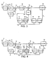
- FIG. 3 shows a further alternative embodiment of the invention.
- phase offset i.e. a phase shift between transmitted symbols
- This phase offset is introduced in order to facilitate implementation of the transmitter architecture.
- the new cellular system EDGE Enhanced Data rates for GSM Evolution
- phase shift phase offset
- the received signal has to be de-rotated.
- a de-rotation of a signal with a DC component gives a signal with a rotating DC component.
- Figure 3 shows a suitable receiver for this situation. Again, components of the circuit of Figure 3 which correspond to those of Figure 1 are given the same reference numerals.
- the first coarse DC estimation and DC subtraction are performed as described above.
- the signal ⁇ 1 (t) is then de-rotated in a de-rotator 32 with a phase shift (- ⁇ ) corresponding to the offset ( ⁇ ) introduced in the transmitter.
- the output ⁇ (t) from the de-rotator 32 is then fed to the first synchronization unit 12 that estimates a synchronization position.
- This position is then fed to the channel estimation unit 14 that estimates the channel filter taps and the residual DC component, taking into account the rotating behaviour of the DC component. This can again be done by using standard Least-Squares estimation techniques.
- the estimate of the residual DC offset is output to a rotation unit 34 that applies an appropriate rotation of the residual DC component, and it is subtracted from the signal ⁇ (t) , giving a signal ⁇ (t) .
- the further processing of the signal ⁇ (t) is carried out as described above.
- control unit that decides whether the second synchronization and channel estimation are to be carried out or not, as described with reference to Figure 2.
- Figure 4 shows a further alternative embodiment of the invention.
- the signal ⁇ (t) is calculated as before using averaging of the received samples over the burst.
- Samples are then differentiated in a differentiator 42, i.e., ⁇ ( t ) - ⁇ ( t- 1) is calculated, and passed on to the synchronization unit 12 which estimates a first synchronization position.
- the differentiation is used in order to reduce the impact of the DC step when doing the first synchronization.
- the synchronization position is then fed to the channel estimation unit 44 together with the undifferentiated samples ⁇ .
- the channel estimation unit now estimates the channel filter taps and the residual DC component, also taking the DC-step into account.
- radio receivers which provide improved synchronization in the presence of a DC offset component.
Landscapes
- Engineering & Computer Science (AREA)
- Computer Networks & Wireless Communication (AREA)
- Signal Processing (AREA)
- Power Engineering (AREA)
- Synchronisation In Digital Transmission Systems (AREA)
- Digital Transmission Methods That Use Modulated Carrier Waves (AREA)
- Crystals, And After-Treatments Of Crystals (AREA)
- Radio Relay Systems (AREA)
- Cable Transmission Systems, Equalization Of Radio And Reduction Of Echo (AREA)
Claims (16)
- Ein Funkempfänger umfassend:einen Front-End-Schaltkreis (4) zum Abtasten eines empfangenen Signals, um ein abgetastetes, empfangenes Signal, das einen Gleichstromversatz enthält, zu erzeugen;einen ersten Versatzberechnungsschaltkreis (8) zum Erzeugen einer ersten Berechnung eines des Gleichstromversatzes aus dem abgetasteten, empfangenen Signal;einen ersten Subtrahierer (10) zum Subtrahieren der ersten Berechnung des Gleichstromversatzes von dem abgetasteten, empfangenen Signal, um ein erstes berechnetes, abgetastetes Signal zu erzeugen;einen ersten Synchronisationsdetektionsschaltkreis (12) zum Berechnen einer Synchronisationsposition des ersten berechneten, abgetasteten Signals;gekennzeichnet durcheinen ersten Kanalberechner (14) zum Erzeugen einer ersten Kanalberechnung auf der Grundlage der bestimmten Synchronisationsposition;einen zweiten Versatzberechnungsschaltkreis (14) zum Erzeugen einer zweiten Berechnung des Gleichstromversatzes aus dem ersten berechneten, abgetasteten Signal nach Bestimmung der Synchronisationsposition; undeinen zweiten Subtrahierer (16) zum Erzeugen eines zweiten berechneten, abgetasteten Signals unter Verwendung des ersten berechneten, abgetasteten Signals und der zweiten Berechnung des Gleichstromversatzes.
- Ein Funkempfänger nach Anspruch 1, wobei das erste berechnete, abgetastete Signal einen Gleichstromrestversatz enthält, wobei der zweite Versatzberechnungsschaltkreis dazu ausgebildet ist, eine Berechnung des Gleichstromrestversatzes zu erzeugen, und der zweite Subtrahierer dazu ausgebildet ist, das zweite berechnete, abgetastete Signal zu erzeugen, indem die Berechnung des Gleichstromrestversatzes von dem ersten berechneten, abgetasteten Signal subtrahiert wird.
- Ein Funkempfänger nach Anspruch 1, ferner umfassend:einen zweitem Synchronisationsdetektionsschaltkreis (18) zum Berechnen einer Synchronisationsposition des zweiten berechneten, abgetasteten Signals;einen zweiten Kanalberechner (20) zum Erzeugen einer zweiten Kanalberechnung auf der Grundlage der zweiten berechneten Synchronisationsposition; undeinen Entzerrer (22) zum Verarbeiten des zweiten berechneten, abgetasteten Signals basiert auf der zweiten Kanalberechnung.
- Ein Funkempfänger nach Anspruch 3, ferner umfassend:eine Steuereinheit (28) zum Bestimmen, ob die Signale auf den zweiten Synchronisationsdetektionsschaltkreis angewendet werden sollen oder nicht und zum Bestimmen der zweiten Kanalberechnung auf der Grundlage einer Berechnung der Signalqualität.
- Ein Funkempfänger nach Anspruch 4, wobei der erste Kanalberechner dazu ausgebildet ist, die Signalqualität zu bestimmen und die Steuereinheit dazu ausgebildet ist, zu bestimmen, dass Signale auf den zweiten Synchronisationsdetektionsschaltkreis aufgebracht werden und der zweite Kanalberechner nur wenn die berechnete Signalqualität einen Schwellwert überschreitet.
- Ein Funkempfänger nach Anspruch 4, wobei, falls die Steuereinheit bestimmt, dass keine Signale auf den zweiten Synchronisationsdetektionsschaltkreis und den zweiten Kanalberechner aufgebracht werden, der Entzerrer dazu ausgebildet ist, die erste Kanalberechnung zu verwenden, um das zweite berechnete, abgetastete Signal zu verarbeiten.
- Ein Funkempfänger nach Anspruch 1, ferner umfassend:eine Entdreheinrichtung bzw. einen Derotator (32), zum Aufbringen einer negativen Drehung auf das erste berechnete, abgetastete Signal; undeine Dreheinrichtung bzw. einen Rotator (34) zum Aufbringen einer Drehung auf die zweite Berechnung des Gleichstromversatzes.
- Ein Funkempfänger nach Anspruch 1, ferner umfassend:einen Differenzierer (42) zum Rechnen eines Differenzialwerts des ersten berechneten, abgetasteten Signals vor dessen Einbringen in den ersten Synchronisationsschaltkreis undeinen Schrittbestimmer (44) zum Bestimmen der Größe eines Gleichstromschritts in dem empfangenen Signal,wobei die zweite Subtrahiereinrichtung dazu ausgebildet ist, die Berechnung der Stärke des Gleichstromschritts von dem ersten berechneten, abgetasteten Signal zu subtrahieren.
- Ein Verfahren zum Verarbeiten eines empfangenen Signals umfassend:Abtasten des empfangenen Signals, um ein abgetastetes empfangenes Signal, das einen Gleichstromversatz enthält, zu erzeugen.Erzeugen einer ersten Berechnung des Gleichstromversatzes aus dem abgetasteten, empfangenen Signal;Subtrahieren der ersten Berechnung des Gleichstromversatzes von dem abgetasteten, empfangenen Signal, um ein erstes berechnetes, abgetastetes Signal zu erzeugen;Berechnen einer Synchronisationsposition des ersten berechneten, abgetasteten Signals;gekennzeichnet durchHerstellen einer ersten Kanalberechnung basiert auf der berechneten Synchronisationsposition;Erzeugen einer zweiten Berechnung des Gleichstromversatzes aus dem ersten berechneten, abgetasteten Signal nach dem Berechnen der Synchronisationsposition; undErzeugen eines zweiten berechneten, abgetasteten Signals unter Verwendung des ersten berechneten, abgetasteten Signals und der zweiten Berechnung des Gleichstromversatzes.
- Ein Verfahren nach Anspruch 9, wobei das erste berechnete, abgetastete Signal einen Gleichstromrestversatz enthält, umfassend Erzeugen einer Berechnung des Gleichstromrestversatzes, und Erzeugen des zweiten berechneten, abgetasteten Signals durch Subtrahieren der Berechnung des Gleichstromrestversatzes von dem ersten berechneten, abgetasteten Signal.
- Ein Verfahren nach Anspruch 9, ferner umfassend:Berechnen einer Synchronisationsposition des zweiten berechneten, abgetasteten Signals;Erzeugen einer zweiten Kanalberechnung auf der Grundlage der zweiten berechneten Synchronisationsposition; undVerarbeiten des zweiten berechneten, abgetasteten Signals in einem Entzerrer basiert auf der zweiten Kanalberechnung.
- Ein Verfahren nach Anspruch 11, ferner umfassend:Bestimmen, ob die Synchronisationsposition des zweiten berechneten, abgetasteten Signals berechnet werden soll oder nicht, und ob die zweite Kanalberechnung erzeugt wird oder nicht auf der Grundlage einer Berechnung der Signalqualität.
- Ein Verfahren nach Anspruch 12, umfassend Berechnen der Signalqualität, und Bestimmen, ob die Synchronisationsposition des zweiten berechneten, abgetasteten Signals berechnet wird, und die zweite Kanalberechnung nur erzeugt wird, wenn die berechnete Signalqualität einen Schwellwert übersteigt.
- Ein Verfahren nach Anspruch 12, umfassend falls bestimmt wird, die Synchronisationsposition des zweiten berechneten, abgetasteten Signals nicht zu berechnen oder die zweite Kanalberechnung nicht zu erzeugen:Verarbeiten des zweiten berechneten, abgetasteten Signals in einem Entzerrer auf der Grundlage der ersten Kanalberechnung.
- Ein Verfahren nach Anspruch 9, ferner umfassend:Aufbringen einer negativen Rotation auf das erste berechnete, abgetastete Signal; undAufbringen einer Rotation auf die zweite Berechnung des Gleichstromversatzes.
- Ein Verfahren nach Anspruch 9, ferner umfassend:Berechnen eines Differenzialwerts des ersten berechneten, abgetasteten Signals vor dessen Aufbringen auf den ersten Synchronisationsschaltkreis, Berechnen der Größe eines Gleichstromschritts in dem empfangenen Signal, undSubtrahieren der Berechnung der Größe des Gleichstromschritts von dem ersten berechneten, abgetasteten Signal.
Applications Claiming Priority (3)
| Application Number | Priority Date | Filing Date | Title |
|---|---|---|---|
| GB9925631 | 1999-10-29 | ||
| GB9925631A GB2355900B (en) | 1999-10-29 | 1999-10-29 | Radio receiver |
| PCT/EP2000/010519 WO2001033792A1 (en) | 1999-10-29 | 2000-10-25 | Radio receiver with two stages of dc offset correction, synchronisation and channel estimation |
Publications (2)
| Publication Number | Publication Date |
|---|---|
| EP1228611A1 EP1228611A1 (de) | 2002-08-07 |
| EP1228611B1 true EP1228611B1 (de) | 2007-05-30 |
Family
ID=10863614
Family Applications (1)
| Application Number | Title | Priority Date | Filing Date |
|---|---|---|---|
| EP00975914A Expired - Lifetime EP1228611B1 (de) | 1999-10-29 | 2000-10-25 | Funkempfänger mit zwei stufen von gleichspannungsverschiebungskorrektur, synchronisation und kanalschätzung |
Country Status (13)
| Country | Link |
|---|---|
| US (1) | US6711393B1 (de) |
| EP (1) | EP1228611B1 (de) |
| JP (1) | JP4536985B2 (de) |
| CN (1) | CN1154310C (de) |
| AR (1) | AR030535A1 (de) |
| AT (1) | ATE363797T1 (de) |
| AU (1) | AU1387101A (de) |
| CO (1) | CO5300373A1 (de) |
| DE (1) | DE60035060T2 (de) |
| ES (1) | ES2284540T3 (de) |
| GB (1) | GB2355900B (de) |
| MY (1) | MY126985A (de) |
| WO (1) | WO2001033792A1 (de) |
Cited By (1)
| Publication number | Priority date | Publication date | Assignee | Title |
|---|---|---|---|---|
| CN101447958B (zh) * | 2008-12-30 | 2011-05-11 | 清华大学 | 一种调制器性能的测量方法和装置 |
Families Citing this family (21)
| Publication number | Priority date | Publication date | Assignee | Title |
|---|---|---|---|---|
| US6941121B2 (en) * | 2001-05-18 | 2005-09-06 | Rf Micro Devices, Inc. | Method for calibrating a DC offset cancellation level for direct conversion receivers |
| US7349680B2 (en) * | 2002-04-29 | 2008-03-25 | Broadcom Corporation | Method and system for using PSK sync word for fine tuning frequency adjustment |
| US7555079B2 (en) * | 2002-11-20 | 2009-06-30 | Telefonaktiebolaget L M Ericsson (Publ) | Method and corresponding arrangement for DC offset compensation using channel estimation |
| EP1429487A3 (de) | 2002-12-09 | 2005-07-20 | Broadcom Corporation | EDGE-Speicherstruktur für inkrementale Redundanz und Speicherverwaltung |
| US7342979B2 (en) | 2002-12-09 | 2008-03-11 | Broadcom Corporation | Incremental redundancy support in a cellular wireless terminal having IR processing module |
| US20060141972A1 (en) * | 2003-02-20 | 2006-06-29 | Nec Corporation | Signal processing device and direct conversion reception device |
| US7342956B2 (en) | 2003-06-16 | 2008-03-11 | Broadcom Corporation | System and method to extract uplink status flag bits in a cellular wireless network |
| US7107080B2 (en) | 2003-06-16 | 2006-09-12 | Broadcom Corporation | System and method to conduct idle mode paging channel monitoring within a cellular wireless network |
| US7068735B2 (en) | 2003-06-16 | 2006-06-27 | Broadcom Corp. | System and method to perform DC compensation on a radio frequency burst in a cellular wireless network |
| US7203461B2 (en) | 2003-06-16 | 2007-04-10 | Broadcom Corporation | Adaptive channel quality estimation algorithm to support link adaptation |
| US7352720B2 (en) | 2003-06-16 | 2008-04-01 | Broadcom Corporation | System and method to determine a bit error probability of received communications within a cellular wireless network |
| US7406139B2 (en) | 2003-06-16 | 2008-07-29 | Broadcom Corporation | System and method to identify a modulation format of a data frame within a cellular wireless network |
| US7277688B2 (en) * | 2003-06-17 | 2007-10-02 | Broadcom Corporation | DC offset correction for very low intermediate frequency receiver |
| US7289583B2 (en) * | 2003-10-14 | 2007-10-30 | Telefonktiebolagel Lm Ericsson (Publ) | Method of and apparatus for single antenna interference rejection through relaxation |
| US7212593B2 (en) * | 2003-10-14 | 2007-05-01 | Telefonaktiebolaget Lm Ericsson (Publ) | Method of and apparatus for noise whitening filtering |
| US7457379B2 (en) | 2003-10-16 | 2008-11-25 | Broadcom Corporation | Adaptive multi-step combined DC offset compensation for EDGE 8-PSK |
| US7366475B2 (en) * | 2004-06-04 | 2008-04-29 | Telefonaktiebolaget Lm Ericsson (Publ) | Signal strength measurements in cellular telecommunication systems |
| GB0419487D0 (en) * | 2004-09-02 | 2004-10-06 | Ttp Communications Ltd | DC estimation in received signals |
| US7817757B2 (en) * | 2006-05-30 | 2010-10-19 | Fujitsu Limited | System and method for independently adjusting multiple offset compensations applied to a signal |
| CN100492026C (zh) * | 2006-12-04 | 2009-05-27 | 北京中星微电子有限公司 | 一种去直流电能计量电路和去直流电路 |
| KR20130104289A (ko) * | 2012-03-13 | 2013-09-25 | 삼성전자주식회사 | 오프셋 값을 추정하는 장치, 방법, 수신장치 및 수신장치에서 신호를 처리하는 방법 |
Family Cites Families (24)
| Publication number | Priority date | Publication date | Assignee | Title |
|---|---|---|---|---|
| DE2738279C3 (de) * | 1977-08-25 | 1980-03-13 | Licentia Patent-Verwaltungs-Gmbh, 6000 Frankfurt | Verfahren und Anordnung zum Ableiten eines Empfangstaktes |
| US5241702A (en) | 1990-09-06 | 1993-08-31 | Telefonaktiebolaget L M Ericsson | D.c. offset compensation in a radio receiver |
| US5319679A (en) | 1992-12-09 | 1994-06-07 | Datum Systems | Method and apparatus for recovering data from a radio signal |
| GB2274759B (en) * | 1993-02-02 | 1996-11-13 | Nokia Mobile Phones Ltd | Correction of D.C offset in received and demodulated radio signals |
| US5724653A (en) * | 1994-12-20 | 1998-03-03 | Lucent Technologies Inc. | Radio receiver with DC offset correction circuit |
| US5798724A (en) | 1996-02-14 | 1998-08-25 | Harris Corporation | Interpolating digital to analog converter architecture for improved spurious signal suppression |
| JP3486058B2 (ja) * | 1996-06-24 | 2004-01-13 | 株式会社東芝 | Dcオフセット除去機能を備えた受信機 |
| US5838735A (en) * | 1996-07-08 | 1998-11-17 | Telefonaktiebolaget Lm Ericsson | Method and apparatus for compensating for a varying d.c. offset in a sampled signal |
| JPH1041992A (ja) * | 1996-07-24 | 1998-02-13 | Nippon Telegr & Teleph Corp <Ntt> | 準同期検波復調装置 |
| WO1998016039A1 (en) | 1996-10-08 | 1998-04-16 | Harris Corporation | Method and apparatus for cancellation of dc offset and reconstruction of low frequency components of baseband signal |
| JP2993443B2 (ja) | 1996-10-31 | 1999-12-20 | 日本電気株式会社 | 通信装置 |
| FI101919B1 (fi) | 1996-11-21 | 1998-09-15 | Nokia Telecommunications Oy | Menetelmä impulssivasteen laskemiseksi ja vastaanotin |
| EP0895385A1 (de) | 1997-07-29 | 1999-02-03 | Alcatel | Verminderung von Gleichstromverschiebungen für Burstbetriebempfang |
| GB2328353B (en) * | 1997-08-16 | 2002-10-02 | Nec Technologies | GSM mobile receiver |
| JP3095067B2 (ja) | 1997-12-04 | 2000-10-03 | 日本電気株式会社 | Dcオフセットキャンセラーおよびこれを備えた受信機と通信システムとdcオフセットキャンセル方法 |
| EP0948128B1 (de) * | 1998-04-03 | 2004-12-01 | Motorola Semiconducteurs S.A. | Unterdrückung von Gleichspannungsverschiebungen in einem Quadraturempfänger |
| KR100314353B1 (ko) * | 1998-04-28 | 2001-12-28 | 전주범 | 직교분할대역수신시스템 |
| EP0964557A1 (de) * | 1998-06-12 | 1999-12-15 | Lucent Technologies Inc. | Empfänger mit Gleichstromoffsetkompensation |
| US6426972B1 (en) * | 1998-06-19 | 2002-07-30 | Nxtwave Communications | Reduced complexity equalizer for multi mode signaling |
| US6263030B1 (en) * | 1998-07-01 | 2001-07-17 | Ericsson Inc. | Equalizer with channel tracker switching |
| US6151328A (en) * | 1998-12-31 | 2000-11-21 | Lg Information & Communications Ltd. | Apparatus and method for controlling power in code division multiple access system |
| US6504884B1 (en) * | 1999-05-12 | 2003-01-07 | Analog Devices, Inc. | Method for correcting DC offsets in a receiver |
| US6463105B1 (en) * | 1999-09-13 | 2002-10-08 | Ericsson Inc. | Methods and systems for estimation of the carrier to interference ratio for a wireless communication channel |
| US20020173286A1 (en) * | 2001-04-06 | 2002-11-21 | Bengt Lindoff | Radiocommunication employing selected synchronization technique |
-
1999
- 1999-10-29 GB GB9925631A patent/GB2355900B/en not_active Expired - Lifetime
-
2000
- 2000-10-24 US US09/695,681 patent/US6711393B1/en not_active Expired - Lifetime
- 2000-10-25 WO PCT/EP2000/010519 patent/WO2001033792A1/en not_active Ceased
- 2000-10-25 JP JP2001534823A patent/JP4536985B2/ja not_active Expired - Lifetime
- 2000-10-25 DE DE60035060T patent/DE60035060T2/de not_active Expired - Lifetime
- 2000-10-25 ES ES00975914T patent/ES2284540T3/es not_active Expired - Lifetime
- 2000-10-25 CN CNB008150915A patent/CN1154310C/zh not_active Expired - Lifetime
- 2000-10-25 AT AT00975914T patent/ATE363797T1/de not_active IP Right Cessation
- 2000-10-25 EP EP00975914A patent/EP1228611B1/de not_active Expired - Lifetime
- 2000-10-25 AU AU13871/01A patent/AU1387101A/en not_active Abandoned
- 2000-10-27 MY MYPI20005052A patent/MY126985A/en unknown
- 2000-10-27 CO CO00081966A patent/CO5300373A1/es not_active Application Discontinuation
- 2000-10-27 AR ARP000105689A patent/AR030535A1/es unknown
Non-Patent Citations (1)
| Title |
|---|
| None * |
Cited By (1)
| Publication number | Priority date | Publication date | Assignee | Title |
|---|---|---|---|---|
| CN101447958B (zh) * | 2008-12-30 | 2011-05-11 | 清华大学 | 一种调制器性能的测量方法和装置 |
Also Published As
| Publication number | Publication date |
|---|---|
| JP4536985B2 (ja) | 2010-09-01 |
| AR030535A1 (es) | 2003-08-27 |
| JP2003513542A (ja) | 2003-04-08 |
| CN1154310C (zh) | 2004-06-16 |
| MY126985A (en) | 2006-11-30 |
| ATE363797T1 (de) | 2007-06-15 |
| AU1387101A (en) | 2001-05-14 |
| WO2001033792A1 (en) | 2001-05-10 |
| CN1385018A (zh) | 2002-12-11 |
| GB2355900A (en) | 2001-05-02 |
| ES2284540T3 (es) | 2007-11-16 |
| DE60035060D1 (de) | 2007-07-12 |
| CO5300373A1 (es) | 2003-07-31 |
| GB2355900B (en) | 2004-03-17 |
| EP1228611A1 (de) | 2002-08-07 |
| GB9925631D0 (en) | 1999-12-29 |
| US6711393B1 (en) | 2004-03-23 |
| DE60035060T2 (de) | 2008-01-24 |
Similar Documents
| Publication | Publication Date | Title |
|---|---|---|
| EP1228611B1 (de) | Funkempfänger mit zwei stufen von gleichspannungsverschiebungskorrektur, synchronisation und kanalschätzung | |
| EP1197049B1 (de) | Verfahren und einrichtung zur durchführung von gleichspannungsoffsetkompensation in einem funkempfänger | |
| KR970007362B1 (ko) | 수신기에서의 손상된 신호 등화 장치 및 방법 | |
| KR100379723B1 (ko) | 디지탈적으로보상된직접변환수신기 | |
| US7187736B2 (en) | Reducing interference in a GSM communication system | |
| CA2407454C (en) | System and method for an in-service decision-directed signal to noise ratio estimator | |
| US6725024B1 (en) | Offset local oscillator frequency | |
| CN101242626B (zh) | 对接收信号进行滤波的设备及方法 | |
| US5550868A (en) | π/4-DQPSK delay spread detection and compensation apparatus and method | |
| EP0838928B1 (de) | Entzerrung von Mehrträgersignalen | |
| US6934346B2 (en) | Apparatus and method for substantially eliminating a near-channel interfering amplitude modulated signal | |
| US7388936B2 (en) | Digital data receiver for edge cellular standard with DC offset correction, channel impulse response estimation, I/Q phase imbalance compensation, interference estimation, and selective equalization | |
| EP1508201B1 (de) | Farb-störungsidentifikation | |
| US20120134454A1 (en) | Apparatus, and associated method, for filtering a receive signal by adaptive operation of an input noise whitening filter | |
| US7664210B2 (en) | Non-coherent synchronous direct-conversion receiving apparatus for compensating frequency offset | |
| US6618453B1 (en) | Estimating interference in a communication system | |
| US7426245B2 (en) | DC compensation in direct conversion radio receivers | |
| US6845133B2 (en) | Method and device for processing signals of a digital transmission system | |
| US20050201490A1 (en) | Zero-crossing detector for receivers | |
| EP1466455B1 (de) | Schätzung eines frequenzfehlers | |
| US7616709B2 (en) | Differential decoder followed by non-linear compensator | |
| KR100813399B1 (ko) | Zero-if 수신기의 i/q부정합 보상 장치 및 그 방법 |
Legal Events
| Date | Code | Title | Description |
|---|---|---|---|
| PUAI | Public reference made under article 153(3) epc to a published international application that has entered the european phase |
Free format text: ORIGINAL CODE: 0009012 |
|
| 17P | Request for examination filed |
Effective date: 20020527 |
|
| AK | Designated contracting states |
Kind code of ref document: A1 Designated state(s): AT BE CH CY DE DK ES FI FR GB GR IE IT LI LU MC NL PT SE |
|
| AX | Request for extension of the european patent |
Free format text: AL;LT;LV;MK;RO;SI |
|
| RAP1 | Party data changed (applicant data changed or rights of an application transferred) |
Owner name: TELEFONAKTIEBOLAGET LM ERICSSON (PUBL) |
|
| RBV | Designated contracting states (corrected) |
Designated state(s): AT BE CH CY DE DK ES FI FR GR IE IT LI LU MC NL PT SE |
|
| GRAP | Despatch of communication of intention to grant a patent |
Free format text: ORIGINAL CODE: EPIDOSNIGR1 |
|
| GRAS | Grant fee paid |
Free format text: ORIGINAL CODE: EPIDOSNIGR3 |
|
| GRAA | (expected) grant |
Free format text: ORIGINAL CODE: 0009210 |
|
| AK | Designated contracting states |
Kind code of ref document: B1 Designated state(s): AT BE CH CY DE DK ES FI FR GR IE IT LI LU MC NL PT SE |
|
| PG25 | Lapsed in a contracting state [announced via postgrant information from national office to epo] |
Ref country code: LI Free format text: LAPSE BECAUSE OF FAILURE TO SUBMIT A TRANSLATION OF THE DESCRIPTION OR TO PAY THE FEE WITHIN THE PRESCRIBED TIME-LIMIT Effective date: 20070530 Ref country code: CH Free format text: LAPSE BECAUSE OF FAILURE TO SUBMIT A TRANSLATION OF THE DESCRIPTION OR TO PAY THE FEE WITHIN THE PRESCRIBED TIME-LIMIT Effective date: 20070530 Ref country code: FI Free format text: LAPSE BECAUSE OF FAILURE TO SUBMIT A TRANSLATION OF THE DESCRIPTION OR TO PAY THE FEE WITHIN THE PRESCRIBED TIME-LIMIT Effective date: 20070530 |
|
| REG | Reference to a national code |
Ref country code: CH Ref legal event code: EP |
|
| REG | Reference to a national code |
Ref country code: IE Ref legal event code: FG4D |
|
| REF | Corresponds to: |
Ref document number: 60035060 Country of ref document: DE Date of ref document: 20070712 Kind code of ref document: P |
|
| REG | Reference to a national code |
Ref country code: SE Ref legal event code: TRGR |
|
| ET | Fr: translation filed | ||
| REG | Reference to a national code |
Ref country code: ES Ref legal event code: FG2A Ref document number: 2284540 Country of ref document: ES Kind code of ref document: T3 |
|
| PG25 | Lapsed in a contracting state [announced via postgrant information from national office to epo] |
Ref country code: AT Free format text: LAPSE BECAUSE OF FAILURE TO SUBMIT A TRANSLATION OF THE DESCRIPTION OR TO PAY THE FEE WITHIN THE PRESCRIBED TIME-LIMIT Effective date: 20070530 |
|
| NLV1 | Nl: lapsed or annulled due to failure to fulfill the requirements of art. 29p and 29m of the patents act | ||
| REG | Reference to a national code |
Ref country code: CH Ref legal event code: PL |
|
| PG25 | Lapsed in a contracting state [announced via postgrant information from national office to epo] |
Ref country code: BE Free format text: LAPSE BECAUSE OF FAILURE TO SUBMIT A TRANSLATION OF THE DESCRIPTION OR TO PAY THE FEE WITHIN THE PRESCRIBED TIME-LIMIT Effective date: 20070530 |
|
| PG25 | Lapsed in a contracting state [announced via postgrant information from national office to epo] |
Ref country code: NL Free format text: LAPSE BECAUSE OF FAILURE TO SUBMIT A TRANSLATION OF THE DESCRIPTION OR TO PAY THE FEE WITHIN THE PRESCRIBED TIME-LIMIT Effective date: 20070530 Ref country code: PT Free format text: LAPSE BECAUSE OF FAILURE TO SUBMIT A TRANSLATION OF THE DESCRIPTION OR TO PAY THE FEE WITHIN THE PRESCRIBED TIME-LIMIT Effective date: 20071030 Ref country code: DK Free format text: LAPSE BECAUSE OF FAILURE TO SUBMIT A TRANSLATION OF THE DESCRIPTION OR TO PAY THE FEE WITHIN THE PRESCRIBED TIME-LIMIT Effective date: 20070530 |
|
| PLBE | No opposition filed within time limit |
Free format text: ORIGINAL CODE: 0009261 |
|
| STAA | Information on the status of an ep patent application or granted ep patent |
Free format text: STATUS: NO OPPOSITION FILED WITHIN TIME LIMIT |
|
| PG25 | Lapsed in a contracting state [announced via postgrant information from national office to epo] |
Ref country code: GR Free format text: LAPSE BECAUSE OF FAILURE TO SUBMIT A TRANSLATION OF THE DESCRIPTION OR TO PAY THE FEE WITHIN THE PRESCRIBED TIME-LIMIT Effective date: 20070831 |
|
| 26N | No opposition filed |
Effective date: 20080303 |
|
| PG25 | Lapsed in a contracting state [announced via postgrant information from national office to epo] |
Ref country code: MC Free format text: LAPSE BECAUSE OF NON-PAYMENT OF DUE FEES Effective date: 20071031 |
|
| PG25 | Lapsed in a contracting state [announced via postgrant information from national office to epo] |
Ref country code: IE Free format text: LAPSE BECAUSE OF NON-PAYMENT OF DUE FEES Effective date: 20071025 |
|
| PG25 | Lapsed in a contracting state [announced via postgrant information from national office to epo] |
Ref country code: CY Free format text: LAPSE BECAUSE OF FAILURE TO SUBMIT A TRANSLATION OF THE DESCRIPTION OR TO PAY THE FEE WITHIN THE PRESCRIBED TIME-LIMIT Effective date: 20070530 |
|
| PG25 | Lapsed in a contracting state [announced via postgrant information from national office to epo] |
Ref country code: LU Free format text: LAPSE BECAUSE OF NON-PAYMENT OF DUE FEES Effective date: 20071025 |
|
| REG | Reference to a national code |
Ref country code: FR Ref legal event code: PLFP Year of fee payment: 16 |
|
| REG | Reference to a national code |
Ref country code: FR Ref legal event code: PLFP Year of fee payment: 17 |
|
| REG | Reference to a national code |
Ref country code: FR Ref legal event code: PLFP Year of fee payment: 18 |
|
| REG | Reference to a national code |
Ref country code: FR Ref legal event code: PLFP Year of fee payment: 19 |
|
| PGFP | Annual fee paid to national office [announced via postgrant information from national office to epo] |
Ref country code: SE Payment date: 20191029 Year of fee payment: 20 Ref country code: DE Payment date: 20191029 Year of fee payment: 20 |
|
| PGFP | Annual fee paid to national office [announced via postgrant information from national office to epo] |
Ref country code: ES Payment date: 20191104 Year of fee payment: 20 Ref country code: IT Payment date: 20191023 Year of fee payment: 20 Ref country code: FR Payment date: 20191025 Year of fee payment: 20 |
|
| REG | Reference to a national code |
Ref country code: DE Ref legal event code: R071 Ref document number: 60035060 Country of ref document: DE |
|
| REG | Reference to a national code |
Ref country code: ES Ref legal event code: FD2A Effective date: 20210205 |
|
| PG25 | Lapsed in a contracting state [announced via postgrant information from national office to epo] |
Ref country code: ES Free format text: LAPSE BECAUSE OF EXPIRATION OF PROTECTION Effective date: 20201026 |