EP1229152A1 - Matériau d'électrode pour former une matrice, couche mince pour former une matrice et procédé de préparation des disques optiques - Google Patents
Matériau d'électrode pour former une matrice, couche mince pour former une matrice et procédé de préparation des disques optiques Download PDFInfo
- Publication number
- EP1229152A1 EP1229152A1 EP02002004A EP02002004A EP1229152A1 EP 1229152 A1 EP1229152 A1 EP 1229152A1 EP 02002004 A EP02002004 A EP 02002004A EP 02002004 A EP02002004 A EP 02002004A EP 1229152 A1 EP1229152 A1 EP 1229152A1
- Authority
- EP
- European Patent Office
- Prior art keywords
- stamper
- forming
- thin film
- film
- electrode material
- Prior art date
- Legal status (The legal status is an assumption and is not a legal conclusion. Google has not performed a legal analysis and makes no representation as to the accuracy of the status listed.)
- Granted
Links
- 239000010409 thin film Substances 0.000 title claims abstract description 67
- 239000007772 electrode material Substances 0.000 title claims abstract description 40
- 230000003287 optical effect Effects 0.000 title claims description 33
- 238000004519 manufacturing process Methods 0.000 title claims description 20
- 229910052737 gold Inorganic materials 0.000 claims abstract description 28
- 239000002075 main ingredient Substances 0.000 claims abstract description 11
- 239000010408 film Substances 0.000 claims description 113
- 239000010949 copper Substances 0.000 claims description 66
- 239000010931 gold Substances 0.000 claims description 66
- 239000010410 layer Substances 0.000 claims description 26
- 239000000463 material Substances 0.000 claims description 26
- 239000000758 substrate Substances 0.000 claims description 26
- 229910052802 copper Inorganic materials 0.000 claims description 25
- 238000005323 electroforming Methods 0.000 claims description 14
- 229910052709 silver Inorganic materials 0.000 claims description 12
- 239000011241 protective layer Substances 0.000 claims description 7
- RYGMFSIKBFXOCR-UHFFFAOYSA-N Copper Chemical compound [Cu] RYGMFSIKBFXOCR-UHFFFAOYSA-N 0.000 claims description 6
- BQCADISMDOOEFD-UHFFFAOYSA-N Silver Chemical compound [Ag] BQCADISMDOOEFD-UHFFFAOYSA-N 0.000 claims description 6
- PCHJSUWPFVWCPO-UHFFFAOYSA-N gold Chemical compound [Au] PCHJSUWPFVWCPO-UHFFFAOYSA-N 0.000 claims description 6
- 239000004332 silver Substances 0.000 claims description 6
- 238000010894 electron beam technology Methods 0.000 claims description 5
- 229920003002 synthetic resin Polymers 0.000 claims description 4
- 239000000057 synthetic resin Substances 0.000 claims description 4
- 238000001746 injection moulding Methods 0.000 claims description 3
- 230000007797 corrosion Effects 0.000 abstract description 37
- 238000005260 corrosion Methods 0.000 abstract description 37
- FAPWRFPIFSIZLT-UHFFFAOYSA-M Sodium chloride Chemical compound [Na+].[Cl-] FAPWRFPIFSIZLT-UHFFFAOYSA-M 0.000 description 18
- 238000000034 method Methods 0.000 description 12
- 239000007769 metal material Substances 0.000 description 11
- PXHVJJICTQNCMI-UHFFFAOYSA-N Nickel Chemical compound [Ni] PXHVJJICTQNCMI-UHFFFAOYSA-N 0.000 description 9
- 239000011780 sodium chloride Substances 0.000 description 9
- 239000000243 solution Substances 0.000 description 8
- 239000000203 mixture Substances 0.000 description 7
- ZAMOUSCENKQFHK-UHFFFAOYSA-N Chlorine atom Chemical compound [Cl] ZAMOUSCENKQFHK-UHFFFAOYSA-N 0.000 description 6
- 239000000460 chlorine Substances 0.000 description 6
- 229910052801 chlorine Inorganic materials 0.000 description 6
- 230000006866 deterioration Effects 0.000 description 6
- 238000007654 immersion Methods 0.000 description 6
- 239000010944 silver (metal) Substances 0.000 description 6
- 238000004544 sputter deposition Methods 0.000 description 6
- 230000000052 comparative effect Effects 0.000 description 5
- PXGOKWXKJXAPGV-UHFFFAOYSA-N Fluorine Chemical compound FF PXGOKWXKJXAPGV-UHFFFAOYSA-N 0.000 description 4
- NINIDFKCEFEMDL-UHFFFAOYSA-N Sulfur Chemical compound [S] NINIDFKCEFEMDL-UHFFFAOYSA-N 0.000 description 4
- 239000005864 Sulphur Substances 0.000 description 4
- 239000011248 coating agent Substances 0.000 description 4
- 238000000576 coating method Methods 0.000 description 4
- 239000011737 fluorine Substances 0.000 description 4
- 229910052731 fluorine Inorganic materials 0.000 description 4
- 238000000059 patterning Methods 0.000 description 4
- 238000001552 radio frequency sputter deposition Methods 0.000 description 4
- 238000005477 sputtering target Methods 0.000 description 4
- KDLHZDBZIXYQEI-UHFFFAOYSA-N Palladium Chemical compound [Pd] KDLHZDBZIXYQEI-UHFFFAOYSA-N 0.000 description 3
- 238000010521 absorption reaction Methods 0.000 description 3
- 230000015572 biosynthetic process Effects 0.000 description 3
- 238000001704 evaporation Methods 0.000 description 3
- 230000008020 evaporation Effects 0.000 description 3
- 229910052751 metal Inorganic materials 0.000 description 3
- 229920000515 polycarbonate Polymers 0.000 description 3
- 239000004417 polycarbonate Substances 0.000 description 3
- 230000035945 sensitivity Effects 0.000 description 3
- 239000000126 substance Substances 0.000 description 3
- 239000011651 chromium Substances 0.000 description 2
- 238000011156 evaluation Methods 0.000 description 2
- 239000011521 glass Substances 0.000 description 2
- 239000011777 magnesium Substances 0.000 description 2
- 238000005259 measurement Methods 0.000 description 2
- 239000010453 quartz Substances 0.000 description 2
- VYPSYNLAJGMNEJ-UHFFFAOYSA-N silicon dioxide Inorganic materials O=[Si]=O VYPSYNLAJGMNEJ-UHFFFAOYSA-N 0.000 description 2
- VYZAMTAEIAYCRO-UHFFFAOYSA-N Chromium Chemical compound [Cr] VYZAMTAEIAYCRO-UHFFFAOYSA-N 0.000 description 1
- DGAQECJNVWCQMB-PUAWFVPOSA-M Ilexoside XXIX Chemical compound C[C@@H]1CC[C@@]2(CC[C@@]3(C(=CC[C@H]4[C@]3(CC[C@@H]5[C@@]4(CC[C@@H](C5(C)C)OS(=O)(=O)[O-])C)C)[C@@H]2[C@]1(C)O)C)C(=O)O[C@H]6[C@@H]([C@H]([C@@H]([C@H](O6)CO)O)O)O.[Na+] DGAQECJNVWCQMB-PUAWFVPOSA-M 0.000 description 1
- FYYHWMGAXLPEAU-UHFFFAOYSA-N Magnesium Chemical compound [Mg] FYYHWMGAXLPEAU-UHFFFAOYSA-N 0.000 description 1
- ZOKXTWBITQBERF-UHFFFAOYSA-N Molybdenum Chemical compound [Mo] ZOKXTWBITQBERF-UHFFFAOYSA-N 0.000 description 1
- KJTLSVCANCCWHF-UHFFFAOYSA-N Ruthenium Chemical compound [Ru] KJTLSVCANCCWHF-UHFFFAOYSA-N 0.000 description 1
- XUIMIQQOPSSXEZ-UHFFFAOYSA-N Silicon Chemical compound [Si] XUIMIQQOPSSXEZ-UHFFFAOYSA-N 0.000 description 1
- 239000000654 additive Substances 0.000 description 1
- 229910052782 aluminium Inorganic materials 0.000 description 1
- XAGFODPZIPBFFR-UHFFFAOYSA-N aluminium Chemical compound [Al] XAGFODPZIPBFFR-UHFFFAOYSA-N 0.000 description 1
- 238000010420 art technique Methods 0.000 description 1
- 238000006243 chemical reaction Methods 0.000 description 1
- 229910052804 chromium Inorganic materials 0.000 description 1
- 239000000470 constituent Substances 0.000 description 1
- 238000000151 deposition Methods 0.000 description 1
- 230000008021 deposition Effects 0.000 description 1
- 238000001035 drying Methods 0.000 description 1
- 238000007772 electroless plating Methods 0.000 description 1
- 239000004615 ingredient Substances 0.000 description 1
- 230000001788 irregular Effects 0.000 description 1
- 239000007788 liquid Substances 0.000 description 1
- 229910052749 magnesium Inorganic materials 0.000 description 1
- 229910052750 molybdenum Inorganic materials 0.000 description 1
- 239000011733 molybdenum Substances 0.000 description 1
- 238000000465 moulding Methods 0.000 description 1
- 229910052759 nickel Inorganic materials 0.000 description 1
- 229910052763 palladium Inorganic materials 0.000 description 1
- 230000010076 replication Effects 0.000 description 1
- 229920005989 resin Polymers 0.000 description 1
- 239000011347 resin Substances 0.000 description 1
- 229910052707 ruthenium Inorganic materials 0.000 description 1
- 229910052710 silicon Inorganic materials 0.000 description 1
- 239000010703 silicon Substances 0.000 description 1
- 239000011734 sodium Substances 0.000 description 1
- 229910052708 sodium Inorganic materials 0.000 description 1
- 238000004528 spin coating Methods 0.000 description 1
- 238000003860 storage Methods 0.000 description 1
- 229910052715 tantalum Inorganic materials 0.000 description 1
- GUVRBAGPIYLISA-UHFFFAOYSA-N tantalum atom Chemical compound [Ta] GUVRBAGPIYLISA-UHFFFAOYSA-N 0.000 description 1
- WFKWXMTUELFFGS-UHFFFAOYSA-N tungsten Chemical compound [W] WFKWXMTUELFFGS-UHFFFAOYSA-N 0.000 description 1
- 229910052721 tungsten Inorganic materials 0.000 description 1
- 239000010937 tungsten Substances 0.000 description 1
- LEONUFNNVUYDNQ-UHFFFAOYSA-N vanadium atom Chemical compound [V] LEONUFNNVUYDNQ-UHFFFAOYSA-N 0.000 description 1
Images

Classifications
-
- C—CHEMISTRY; METALLURGY
- C25—ELECTROLYTIC OR ELECTROPHORETIC PROCESSES; APPARATUS THEREFOR
- C25D—PROCESSES FOR THE ELECTROLYTIC OR ELECTROPHORETIC PRODUCTION OF COATINGS; ELECTROFORMING; APPARATUS THEREFOR
- C25D1/00—Electroforming
- C25D1/10—Moulds; Masks; Masterforms
-
- B—PERFORMING OPERATIONS; TRANSPORTING
- B81—MICROSTRUCTURAL TECHNOLOGY
- B81C—PROCESSES OR APPARATUS SPECIALLY ADAPTED FOR THE MANUFACTURE OR TREATMENT OF MICROSTRUCTURAL DEVICES OR SYSTEMS
- B81C99/00—Subject matter not provided for in other groups of this subclass
- B81C99/0075—Manufacture of substrate-free structures
- B81C99/009—Manufacturing the stamps or the moulds
-
- B—PERFORMING OPERATIONS; TRANSPORTING
- B81—MICROSTRUCTURAL TECHNOLOGY
- B81C—PROCESSES OR APPARATUS SPECIALLY ADAPTED FOR THE MANUFACTURE OR TREATMENT OF MICROSTRUCTURAL DEVICES OR SYSTEMS
- B81C2201/00—Manufacture or treatment of microstructural devices or systems
- B81C2201/01—Manufacture or treatment of microstructural devices or systems in or on a substrate
- B81C2201/0101—Shaping material; Structuring the bulk substrate or layers on the substrate; Film patterning
- B81C2201/0128—Processes for removing material
-
- B—PERFORMING OPERATIONS; TRANSPORTING
- B81—MICROSTRUCTURAL TECHNOLOGY
- B81C—PROCESSES OR APPARATUS SPECIALLY ADAPTED FOR THE MANUFACTURE OR TREATMENT OF MICROSTRUCTURAL DEVICES OR SYSTEMS
- B81C2201/00—Manufacture or treatment of microstructural devices or systems
- B81C2201/03—Processes for manufacturing substrate-free structures
- B81C2201/032—LIGA process
Definitions
- the present invention relates to a stamper-forming thin film used to form a stamper which is a mold for mass production of optical disks such as compact disks (CDs) and digital versatile disks (DVDs), and to a stamper-forming electrode material for making the stamper-forming thin film. More particularly, the invention is directed to a stamper-forming thin film used as an electrode for forming the stamper by electroforming, and to a stamper-forming electrode material for making the electrode. The invention also relates to a method of manufacturing optical disks such as CDs or DVDs using the stamper.
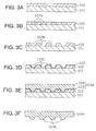
- a resist film 102 is formed by spin coating or the like on a polished, smooth and flat surface of a supporting plate 101 made of glass. Then, this resist film 102 is patterned. For the patterning, as shown in FIG. 3B, the resist film 102 is exposed to a laser beam to form a latent image 102a, which is thereafter developed. As a result, a pattern 102b of grooves, or otherwise referred to as a grooved pattern 102b, is formed in the surface of the resist film 102, as shown in FIG. 3C.
- an electrode film 103 made of a metallic material is deposited on the resist film 102 by sputtering, evaporation, or the like in a manner applying a coating over the entire part of the grooved pattern 102b.
- the electrode film 103 is made of a single metallic material, nickel (Ni), which is highly conductive and hard to change in composition after film formation, into a uniform thickness.
- Ni nickel
- FIG. 3E a Ni metallic layer 104 is stacked on the electrode film 103 by electroforming using the film 103 as an electrode.
- the metallic layer 104 is separated, together with the electrode film 103, from the surface of the resist film 102 to produce a stamper 104a which is a monolithic member consisting of the electrode film 103 and the metallic layer 104.
- a surface of the stamper 104a has a pattern 104b of projections, or otherwise referred to as a projected pattern 104b, which has been transferred as the inverse of the grooved pattern 102b.
- a synthetic resin material is injected into the stamper 104a as a mold toward its projected pattern 104b, to form a substrate on which a grooved pattern exactly identical with the grooved pattern 102b has been copied. Thereafter, a reflector film, a protective layer, etc. are stacked on the substrate in a manner coating the copied grooved pattern, to complete the manufacture of an optical disk.
- an electron beam is replacing a laser beam during the patterning to implement a narrower groove width, for formation of a higher-definition grooved pattern 102b.
- electron-attracting elements such as chlorine, sulphur and fluorine, groups having an electron-attracting function (electron-attracting groups) or the like are added to a resist material for forming the resist film 102b, to provide the resist film 102b with improved electron absorption sensitivity.
- the use of the resist film 102 with improved electron absorption sensitivity may cause damage, such as deterioration, to the electrode film 103 during electroforming for stacking the metallic layer 104 on the electrode film 103, due to Ni in the electrode film 103 reacting with the electron-attracting elements or groups.
- the damaged electrode film 103 roughens the surface of the projected pattern 104b of the stamper 104a.
- such a stamper 104a cannot transfer the grooved pattern 102b to the substrate accurately, resulting in replication of low-performance optical disks with low signal-to-noise ratio (SNR) due to greater noise during data reading.
- SNR signal-to-noise ratio
- An object of the invention is, therefore, to provide a stamper-forming electrode material and a stamper-forming thin film with improved corrosion resistance to suppress damage to the stamper-forming thin film and hence allow a high-quality stamper to be formed.
- Another object of the invention is to provide a method of manufacturing an optical disk with improved SNR and hence with high performance by improving the corrosion resistance of the stamper-forming thin film to suppress damage to the stamper-forming thin film and hence allow a high-quality stamper to be formed.
- the above object of the present invention can be achieved by a stamper-forming thin film of the present invention to be coated on a surface of a resist film patterned on a supporting plate.
- the stamper-forming thin film is provided with a stamper-forming electrode material for forming a stamper by stacking a metallic layer on a surface of said stamper-forming thin film by electroforming using said stamper-forming thin film as an electrode, and thereafter by separating said metallic layer from said resist film, together with said stamper-forming thin film.
- the material contains silver (Ag) as a main ingredient thereof and at least one other element.
- said other element is at least one of gold (Au) and copper (Cu).
- said material contains Au in an amount of 5.0 wt% or less.
- said material contains Cu in an amount of 5.0 wt% or less.
- the above object of the present invention can be achieved by a stamper-forming thin film of the present invention to be coated on a surface of a resist film patterned on a supporting plate.
- the stamper-forming thin film is provided with a stamper-forming electrode material for forming a stamper by stacking a metallic layer on a surface of said stamper-forming thin film by electroforming using said stamper-forming thin film as an electrode, and thereafter by separating said metallic layer from said resist film, together with said stamper-forming thin film.
- said material contains silver (Ag) as a main ingredient thereof and at least one other element.
- said other element is at least one of gold (Au) and copper (Cu).
- said material contains Au in an amount of 5.0 wt% or less.
- said material contains Cu in an amount of 5.0 wt% or less.
- the above object of the present invention can be achieved by a method of manufacturing an optical disk of the present invention.
- the method is provided with the steps of: forming a resist film on a surface of a supporting plate; forming a predetermined pattern on said resist film by exposure to an electron beam; forming a stamper-forming thin film made of a stamper-forming electrode material on a surface of said patterned resist film; stacking a metallic layer on a surface of said stamper-forming thin film by electroforming using said stamper-forming thin film as an electrode, and thereafter by separating said metallic layer from said resist film, together with said stamper-forming thin film, to form a stamper; injection-molding a substrate made of a synthetic resin using said stamper as a mold; and stacking a reflector film and a protective layer on a surface of said substrate to manufacture said optical disk.
- said stamper-forming electrode material of which said stamper-forming thin film is made contains Ag as a main ingredient thereof, and has at least one other element added to Ag.
- the corrosion resistance of a stamper-forming thin film is improved to suppress damage to the stamper-forming thin film and hence allow a high-quality stamper to be formed, whereby an optical disk can be manufactured which has improved SNR and hence maintains high performance.
- said other element is at least one of gold (Au) and copper (Cu).
- said material contains Au in an amount of 5.0 wt% or less.
- said material contains Cu in an amount of 5.0 wt% or less.
- a substrate 21, which constitutes an optical disk 20 is a transparent disk-shaped member made of a synthetic resin (polycarbonate), and its upper surface contains a pattern 21a of tiny grooves, or otherwise referred to as a grooved pattern 21a.
- a reflector film 22, which is an aluminum (Al) thin film is stacked in a manner coating each groove of the pattern 21a.
- a protective layer 23 made of a UV curable resin is stacked in a manner applying a coating over the entire surface of the substrate 21 while burying each groove of the pattern 21a. The protective layer 23 protects both the grooved pattern 21a and the reflector film 22 against damage.
- the substrate 21 is formed using a metallic stamper 15 molded by a method to be described below.
- the stamper 15 is formed into a monolithic member by stacking an electrode film 13 on a Ni metallic layer 14.
- the electrode film 13 is a stamper-forming thin film made of a metallic material (stamper-forming electrode material) and is formed below the metallic layer 14.
- the lower surface of the stamper 15 has a pattern 16 of projections, or otherwise referred to as a projected pattern 16, which is the inverse of the grooved pattern 21a provided in the substrate 21.
- a polycarbonate material is injected into the stamper 15 as a mold toward the projected groove 16 on its lower surface, and the polycarbonate part is then released from the stamper 15 after hardened.
- the reflector film 22 is deposited on the injection-molded substrate 21 by sputtering, evaporation or the like, and then the protective layer 23 is formed on the reflector film 22.
- a resist film 12 is formed on a supporting plate 11.
- a polished, cleaned, smooth and flat surface of the supporting plate 11 made of a glass plate or a silicon wafer is, for example, spin-coated with a liquid resist material to a uniform thickness, and then prebaked for drying the resist material to form the resist film 12 thereon.
- the resist material contains electron-attracting elements such as chlorine, sulphur and fluorine, or electron-attracting groups, and thus the deposited resist film 12 has improved electron absorption sensitivity.
- the resist film 12 is patterned. As shown in FIG. 1B, the resist film 12 is exposed to an electron beam from top to form a latent image 12a on its surface, whereby data signals are recorded. Then, as shown in FIG. 1C, the resist film 12 is developed to remove the latent image 12a portion, whereby a pattern 12b of grooves, or a grooved pattern 12b, is provided therein. Successively, the resultant resist film 12 is postbaked to complete its patterning step.
- the electrode film 13 made of the stamper-forming electrode material (metallic material) as the stamper-forming thin film is deposited on the upper surface of the resist film 12 to a uniform thickness by a process such as sputtering, evaporation, or electroless plating.
- a process such as sputtering, evaporation, or electroless plating.
- the shape of the grooved pattern 12b has been accurately transferred to the electrode film 13.
- the stamper 15 is formed. As shown in FIG. 1E, electroforming is performed using the electrode film 13 as an electrode to deposit Ni on the electrode film 13 as the metallic layer 14. Thereafter, this metallic layer 14 is separated, together with the electrode film 13, from the surface of the resist film 12 and supporting plate 11, to obtain the stamper 15 in the form of a monolithic member consisting of the metallic layer 14 and the electrode film 13, as shown in FIG. 1F.
- the lower surface of the stamper 15 is provided, through the electrode film 13, with the projected pattern 16 which is the exact opposite of the grooved pattern 12b accurately transferred to the electrode film 13.
- This stamper 15 is thus used to injection-mold the substrate 21 that constitutes the optical disk 20, as mentioned above.
- the stamper 15 may subsequently be used as a master stamper to prepare a submaster stamper having the grooved pattern, by electroforming its surface provided with the projected pattern 16. Thereafter, a plurality of baby stampers each being identical in shape with the master stamper are prepared using the submaster stamper, to replicate the substrates 21 of optical disks 20 by injection molding.
- the stamper-forming electrode material (metallic material) for making the electrode film 13 contains silver (Ag) as its main ingredient, and at least one other element. Silver is contained because it is highly conductive and less susceptible to chemical reaction with the electron-attracting elements or groups present in the resist material.
- the term "main ingredient” herein means an ingredient contained most in the stamper-forming electrode material.
- the at least one other element is selected preferably from gold (Au) and copper (Cu) which can easily improve the corrosion resistance of the electrode film 13 as the stamper-forming thin film.
- At least one element may be selected from Al, palladium (Pd), Ni, vanadium (V), tantalum (Ta), tungsten (W), molybdenum (Mo), chromium (Cr), ruthenium (Ru), and magnesium (Mg).
- the stamper-forming electrode material according to this embodiment contains Ag as its main ingredient, and Au and Cu selected from the above-listed metallic elements as additives.
- the addition of Au and Cu to the stamper-forming electrode material contributes to improving the corrosion resistance of the electrode film 13 to electron-attracting elements such as chlorine, sulphur and fluorine, or substances containing such elements as electron-attracting groups, while maintaining the conductivity of the film 13.
- the element Au is added to the stamper-forming electrode material preferably in an amount of 5.0 percent by weight (wt%) or less, more preferably 3.0 wt% or less, or even more preferably 1.5 wt% or less.
- the Au content greater than 5.0 wt% may make Au hard to form colloidal mixtures with Ag and Cu depending on how they are contained to compose the material, or may produce a metallic material with unstable properties or with an undesired corrosion resistance.
- the Cu content in the stamper-forming electrode material is set preferably to 5.0 wt% or less, more preferably to 3.0 wt% or less, or even more preferably to 1.5 wt% or less.
- the Cu content greater than 5.0 wt% may make Cu hard to form colloidal mixtures with Ag and Au depending on how they are contained to compose the material, or may produce a metallic material with unstable properties or with an undesired corrosion resistance.
- the electrode film 13 as the stamper-forming thin film according to the embodiment is made of the stamper-forming electrode material (metallic material) containing Ag, Au, and Cu.
- This material containing Ag, Au, and Cu due to its high corrosion resistance to electron-attracting elements such as chlorine, sulphur and fluorine, or substances having such elements as electron-attracting groups, prevents damage, such as deterioration, to the electrode film 13 during formation of the Ni metallic layer 14 by electroforming.
- the substrate 21 of the optical disk 20 prepared by such a stamper 15 is provided with the grooved pattern 21a exactly identical with the grooved pattern 12b of the resist film 12, as well as smooth and planar inside surfaces in the grooves of the pattern 21a.
- These smooth and planar surfaces suppress irregular reflection of laser light emitted from an optical pickup for reading data recorded on the optical disk 20, to improve the signal-to-noise ratio (SNR), whereby the optical disk 20 can maintain high performance.
- Both the Au and Cu contents in the stamper-forming electrode material are set to 5.0 wt% or less, whereby the corrosion resistance of the electrode film 13 can be further improved synergistically.
- Electrode films 13 containing Ag, Au, and Cu were formed on quartz substrates using an RF sputtering system. Specifically, three kinds of sputtering targets, Au, Ag, and Cu, were disposed in the RF sputtering system for simultaneous deposition on the respective substrates by sputtering to form the electrode films 13 on the substrates. Each sputtering target was 7.62 cm (3 inches) in diameter and 5 mm in thickness, and its distance to the substrate was about 90 cm. The films were formed under a vacuum of 3 ⁇ 10 -5 Pa, a gas pressure of 0.7-1.0 Pa, and an RF power of 100-500W.
- the Au content was varied while the Cu content was fixed at 0.1 wt% to form the electrode film 13.
- the contents of these elements were adjusted by controlling ejection of their metallic atoms, while the ejection control was performed by adjusting RF power to be applied to the respective sputtering targets.
- An electrode film 13 consisting only of Ag was formed on a quartz substrate using the RF sputtering system.
- An Ag sputtering target which was 7.62 (3 inches) in diameter and 5 mm in thickness, was disposed in the RF sputtering system to be sputtered at a distance of about 90 cm to the substrate.
- the film was formed under a vacuum of 3 ⁇ 10 -5 Pa, a gas pressure of 0.7-1.0 Pa, and an RF power of 100-500W.
- the electrode films 13 obtained as Examples 1 to 6 and Comparative Example 1 were immersed in an aqueous sodium chloride (NaCl) solution whose concentration was 5 percent by volume (vol%), together with the quarts substrates at room temperature for predetermined times, for evaluation to see if they changed with time.
- Table 1 shows the results.
- the chemical composition of each metallic material, i.e., the contents of its constituent metallic elements are indicated on a wt% basis.
- the changes with time were visibly evaluated by those responsible for measurement.
- G denotes no deterioration on the electrode film 13 surface
- "OK” denotes slight deterioration on the electrode film 13 surface
- NG denotes deterioration on the electrode film 13 surface, during measurement.
- aqueous NaCl solution was used to verify the assumption that chlorine and sodium to be contained in an arbitrarily selected resist material would corrode the electrode film 13.
- Sample No. Composition (wt%) Result from immersion in aqueous NaCl solution Ag Au Cu
- Example 1 99.8 0.1 0.1 G
- Example 2 99.2 0.7 0.1 G
- Example 3 98.4 1.5 0.1 G
- Example 4 96.9 3.0 0.1 G
- Example 5 94.9 5.0 0.1 G
- Example 6 93.9 6.0 0.1 NG Comparative Example 1 100 0 0 NG
- Comparative Example 1 deteriorated to have the entire end of its electrode film 13 surface turned yellow when immersed in the aqueous NaCl solution.
- Example 6 its electrode film 13 deteriorated to have part of the end of the surface slightly turned yellow.
- Examples 1 to 5 exhibited no deterioration on the surfaces of their electrode films 13 from immersion in the aqueous NaCl solution.
- addition of Au and Cu to the metallic material contributes to improving corrosion resistance.
- the surface of the electrode film 13 did not deteriorate in each of Examples 1 to 5, but slightly deteriorated in Example 6.
- the Au content should be set preferably to 5.0 wt% or less, and further that the Au content should be set preferably to 1 to 50 times the Cu content when the Ag content is 94-99.9 wt%. Based on these teachings, an optimum Cu content for preparing an electrode film 13 was sought in the following examples.
- Electro films 13 were formed by sputtering Ag, Au, and Cu, while controlling ejection of their metallic atoms similarly to Examples 1 to 6, provided that the Cu content was varied with the Au content fixed at 5.0 wt%.
- the obtained electrode films 13 were similarly evaluated for their corrosion resistance. Table 2 shows the results.
- Sample No. Composition (wt%) Result from immersion in aqueous NaCl solution Ag Au Cu
- Example 7 94.3 5.0 0.7 G
- Example 8 93.5 5.0 1.5 G
- Example 10 90 5.0 5.0 G
- Example 11 89 5.0 6.0 NG
- Example 11 the surfaces of their electrode films 13 did not deteriorate from immersion in the aqueous NaCl solution.
- the surface of its electrode film 13 deteriorated to have part of the end of the surface slightly turned yellow. That is, the surface of the electrode film 13 did not deteriorate in each of Examples 7 to 10, but slightly deteriorated in Example 11 when the Cu content was varied over the range 0.7-6.0 wt% with the Au content unvaried.
- the Cu content should be set preferably to 5.0 wt% or less, and further that the Au content should be set preferably to 1.0 to 7.5 times the Cu content when the Ag content is 90-95.0 wt%,
- electrode films 13 were formed by sputtering Ag, Au, and Cu, while controlling ejection of their metallic atoms similarly to Examples 1 to 6, provided that the Cu content was varied with the Au content fixed at 0.5 wt% for Examples 12 to 16 and that the Au content was varied with the Cu content fixed at 0.5 wt% for Examples 17 and 18.
- the obtained electrode films 13 were similarly evaluated for their corrosion resistance while immersed in a 5 vol.% aqueous NaCl solution at room temperature for 5, 10, and 24 hours. Table 3 shows the results. Sample No.
- Example 12 the surface of its electrode film 13 did not deteriorate when immersed for 5 hours, but deteriorated when immersed for 10 hours.
- Example 13 and 14 the surfaces of their electrode films 13 did not deteriorate when immersed for 5 to 10 hours, but deteriorated when immersed for 24 hours.
- Example 13 had a higher corrosion resistance than Example 12 despite the fact that both contained 0.5 wt% Au. This suggests that the Cu content be set more preferably to 3.5 wt% or less when the Au content is 0.5 wt%.
- Example 15 had a higher corrosion resistance than Example 14 despite the fact that both contained 0.5 wt% Au. This further suggests that the Cu content be set even more preferably to 1.5 wt% or less when the Au content is 0.5 wt%. It is also taught that the Cu content should be 1 to 3 times the Au content when the Ag content is 98-99 wt%,
- both Examples 17 and 18 wherein the Cu content was fixed at 0.5 wt% exhibited an extremely high corrosion resistance. This suggests that the best corrosion resistance be given when the Cu content is set to 0.5 wt% or less and the Au content to 5.0 wt% or less. It is further taught that the Au content should be set preferably to 6 to 10 times the Cu content when the Ag content is 94-97 wt%.
- this embodiment may be modified as follows.
- the substrate 21, the reflector film 22, and the protective layer 23 although the optical disk 20 according to this embodiment includes only one layer each, an optical disk 20 may also include two or more layers each.
Landscapes
- Engineering & Computer Science (AREA)
- Chemical & Material Sciences (AREA)
- Manufacturing & Machinery (AREA)
- Microelectronics & Electronic Packaging (AREA)
- Chemical Kinetics & Catalysis (AREA)
- Electrochemistry (AREA)
- Materials Engineering (AREA)
- Metallurgy (AREA)
- Organic Chemistry (AREA)
- Moulds For Moulding Plastics Or The Like (AREA)
- Manufacturing Optical Record Carriers (AREA)
Applications Claiming Priority (4)
| Application Number | Priority Date | Filing Date | Title |
|---|---|---|---|
| JP2001028456 | 2001-02-05 | ||
| JP2001028457 | 2001-02-05 | ||
| JP2001028456A JP4431286B2 (ja) | 2001-02-05 | 2001-02-05 | スタンパ形成用電極材料及びスタンパ形成用薄膜 |
| JP2001028457A JP4431287B2 (ja) | 2001-02-05 | 2001-02-05 | 光ディスクの製造方法 |
Publications (2)
| Publication Number | Publication Date |
|---|---|
| EP1229152A1 true EP1229152A1 (fr) | 2002-08-07 |
| EP1229152B1 EP1229152B1 (fr) | 2006-09-06 |
Family
ID=26608932
Family Applications (1)
| Application Number | Title | Priority Date | Filing Date |
|---|---|---|---|
| EP02002004A Expired - Lifetime EP1229152B1 (fr) | 2001-02-05 | 2002-02-05 | Utilisation d'un matériau d'électrode pour former une matrice, utilisation d'une couche mince pour former une matrice et procédé de préparation de disques optiques |
Country Status (3)
| Country | Link |
|---|---|
| US (1) | US20020153625A1 (fr) |
| EP (1) | EP1229152B1 (fr) |
| DE (1) | DE60214447T2 (fr) |
Cited By (3)
| Publication number | Priority date | Publication date | Assignee | Title |
|---|---|---|---|---|
| EP1400330A1 (fr) * | 2002-09-06 | 2004-03-24 | Hewlett-Packard Development Company, L.P. | Procédé et dispositif pour la fabrication de films et de membranes avec une grande surface spécifique |
| EP1413923A3 (fr) * | 2002-10-24 | 2006-05-17 | Hewlett-Packard Development Company, L.P. | Tampon pour la nanolithographie par impression |
| EP1617428A4 (fr) * | 2003-04-18 | 2008-08-20 | Pioneer Corp | Matrice de pressage et son procede de production |
Families Citing this family (3)
| Publication number | Priority date | Publication date | Assignee | Title |
|---|---|---|---|---|
| US20050221112A1 (en) * | 2004-03-31 | 2005-10-06 | Daewoong Suh | Microtools for package substrate patterning |
| US8178011B2 (en) * | 2009-07-29 | 2012-05-15 | Empire Technology Development Llc | Self-assembled nano-lithographic imprint masks |
| JP6648015B2 (ja) * | 2014-06-17 | 2020-02-14 | 日本碍子株式会社 | セラミックスデバイス、及び接合体 |
Citations (3)
| Publication number | Priority date | Publication date | Assignee | Title |
|---|---|---|---|---|
| US4661212A (en) * | 1985-10-22 | 1987-04-28 | Kernforschungszentrum Kalrsruhe Gmbh | Method for producing a plurality of plate shaped microstructured metal bodies |
| US5073237A (en) * | 1990-04-03 | 1991-12-17 | Kernforschungszentrum Karlsruhe Gmbh | Method of making molds for electrodeposition forming of microstructured bodies |
| EP0561080A1 (fr) * | 1992-03-16 | 1993-09-22 | Pioneer Electronic Corporation | Photoréserve pour disque optique et procédé pour la fabrication d'un disque optique utilisant cette photoréserve |
Family Cites Families (2)
| Publication number | Priority date | Publication date | Assignee | Title |
|---|---|---|---|---|
| EP0089168B1 (fr) * | 1982-03-15 | 1986-07-23 | Kabushiki Kaisha Toshiba | Support d'enregistrement d'information par voie optique |
| JPS61133349A (ja) * | 1984-12-03 | 1986-06-20 | Hitachi Ltd | 分光反射率可変合金及び記録材料 |
-
2002
- 2002-02-04 US US10/061,222 patent/US20020153625A1/en not_active Abandoned
- 2002-02-05 DE DE60214447T patent/DE60214447T2/de not_active Expired - Lifetime
- 2002-02-05 EP EP02002004A patent/EP1229152B1/fr not_active Expired - Lifetime
Patent Citations (3)
| Publication number | Priority date | Publication date | Assignee | Title |
|---|---|---|---|---|
| US4661212A (en) * | 1985-10-22 | 1987-04-28 | Kernforschungszentrum Kalrsruhe Gmbh | Method for producing a plurality of plate shaped microstructured metal bodies |
| US5073237A (en) * | 1990-04-03 | 1991-12-17 | Kernforschungszentrum Karlsruhe Gmbh | Method of making molds for electrodeposition forming of microstructured bodies |
| EP0561080A1 (fr) * | 1992-03-16 | 1993-09-22 | Pioneer Electronic Corporation | Photoréserve pour disque optique et procédé pour la fabrication d'un disque optique utilisant cette photoréserve |
Cited By (5)
| Publication number | Priority date | Publication date | Assignee | Title |
|---|---|---|---|---|
| EP1400330A1 (fr) * | 2002-09-06 | 2004-03-24 | Hewlett-Packard Development Company, L.P. | Procédé et dispositif pour la fabrication de films et de membranes avec une grande surface spécifique |
| US6946362B2 (en) | 2002-09-06 | 2005-09-20 | Hewlett-Packard Development Company, L.P. | Method and apparatus for forming high surface area material films and membranes |
| EP1413923A3 (fr) * | 2002-10-24 | 2006-05-17 | Hewlett-Packard Development Company, L.P. | Tampon pour la nanolithographie par impression |
| EP1617428A4 (fr) * | 2003-04-18 | 2008-08-20 | Pioneer Corp | Matrice de pressage et son procede de production |
| CN1774752B (zh) * | 2003-04-18 | 2010-04-28 | 日本先锋公司 | 压模及其制造方法 |
Also Published As
| Publication number | Publication date |
|---|---|
| EP1229152B1 (fr) | 2006-09-06 |
| DE60214447T2 (de) | 2007-08-30 |
| US20020153625A1 (en) | 2002-10-24 |
| DE60214447D1 (de) | 2006-10-19 |
Similar Documents
| Publication | Publication Date | Title |
|---|---|---|
| US5051340A (en) | Master for optical element replication | |
| EP1229152A1 (fr) | Matériau d'électrode pour former une matrice, couche mince pour former une matrice et procédé de préparation des disques optiques | |
| US6849390B2 (en) | Stamper-forming electrode material, stamper-forming thin film, and method of manufacturing optical disk | |
| KR20050090392A (ko) | 수지 성형용 금형 및 수지 성형용 금형의 제조방법 | |
| CN1174402C (zh) | 用来制作压模的电极材料和薄膜 | |
| KR100597554B1 (ko) | 광디스크의 제조 방법 | |
| CN1042259A (zh) | 光学记录介质和其制造方法 | |
| KR100817566B1 (ko) | 스탬퍼, 및 그 제조 방법 | |
| JP4431287B2 (ja) | 光ディスクの製造方法 | |
| KR20050000310A (ko) | 광 정보 기록매체의 스탬퍼의 제조방법 | |
| JP2002230848A (ja) | スタンパ形成用電極材料及びスタンパ形成用薄膜 | |
| JP4431286B2 (ja) | スタンパ形成用電極材料及びスタンパ形成用薄膜 | |
| JP2002230849A (ja) | 光ディスクの製造方法 | |
| CN1777841A (zh) | 光刻工艺、压模、该压模的使用以及光学数据存储介质 | |
| JP2003006947A5 (fr) | ||
| JPS6148146A (ja) | 光デイスク用スタンパ | |
| HK1099118A (en) | Production method for optical disc | |
| JPH04139632A (ja) | 情報記録媒体作成用スタンパーの製造方法 | |
| JPH0827997B2 (ja) | 光ディスク用スタンパー | |
| JPH02106747A (ja) | 記録原板の製造方法 |
Legal Events
| Date | Code | Title | Description |
|---|---|---|---|
| PUAI | Public reference made under article 153(3) epc to a published international application that has entered the european phase |
Free format text: ORIGINAL CODE: 0009012 |
|
| AK | Designated contracting states |
Kind code of ref document: A1 Designated state(s): AT BE CH CY DE DK ES FI FR GB GR IE IT LI LU MC NL PT SE TR |
|
| AX | Request for extension of the european patent |
Free format text: AL;LT;LV;MK;RO;SI |
|
| 17P | Request for examination filed |
Effective date: 20020822 |
|
| 17Q | First examination report despatched |
Effective date: 20021004 |
|
| AKX | Designation fees paid |
Designated state(s): DE FR GB |
|
| GRAP | Despatch of communication of intention to grant a patent |
Free format text: ORIGINAL CODE: EPIDOSNIGR1 |
|
| RTI1 | Title (correction) |
Free format text: USE OF STAMPER-FORMING ELECTRODE MATERIAL, USE OF STAMPER-FORMING THIN FILM, AND METHOD OF MANUFACTURING OPTICAL DISK |
|
| GRAS | Grant fee paid |
Free format text: ORIGINAL CODE: EPIDOSNIGR3 |
|
| GRAA | (expected) grant |
Free format text: ORIGINAL CODE: 0009210 |
|
| AK | Designated contracting states |
Kind code of ref document: B1 Designated state(s): DE FR GB |
|
| REG | Reference to a national code |
Ref country code: GB Ref legal event code: FG4D |
|
| REF | Corresponds to: |
Ref document number: 60214447 Country of ref document: DE Date of ref document: 20061019 Kind code of ref document: P |
|
| REG | Reference to a national code |
Ref country code: GB Ref legal event code: 746 Effective date: 20070123 |
|
| ET | Fr: translation filed | ||
| PLBE | No opposition filed within time limit |
Free format text: ORIGINAL CODE: 0009261 |
|
| STAA | Information on the status of an ep patent application or granted ep patent |
Free format text: STATUS: NO OPPOSITION FILED WITHIN TIME LIMIT |
|
| 26N | No opposition filed |
Effective date: 20070607 |
|
| PGFP | Annual fee paid to national office [announced via postgrant information from national office to epo] |
Ref country code: FR Payment date: 20100223 Year of fee payment: 9 |
|
| PGFP | Annual fee paid to national office [announced via postgrant information from national office to epo] |
Ref country code: DE Payment date: 20100211 Year of fee payment: 9 Ref country code: GB Payment date: 20100202 Year of fee payment: 9 |
|
| GBPC | Gb: european patent ceased through non-payment of renewal fee |
Effective date: 20110205 |
|
| REG | Reference to a national code |
Ref country code: FR Ref legal event code: ST Effective date: 20111102 |
|
| PG25 | Lapsed in a contracting state [announced via postgrant information from national office to epo] |
Ref country code: FR Free format text: LAPSE BECAUSE OF NON-PAYMENT OF DUE FEES Effective date: 20110228 |
|
| REG | Reference to a national code |
Ref country code: DE Ref legal event code: R119 Ref document number: 60214447 Country of ref document: DE Effective date: 20110901 |
|
| PG25 | Lapsed in a contracting state [announced via postgrant information from national office to epo] |
Ref country code: GB Free format text: LAPSE BECAUSE OF NON-PAYMENT OF DUE FEES Effective date: 20110205 |
|
| PG25 | Lapsed in a contracting state [announced via postgrant information from national office to epo] |
Ref country code: DE Free format text: LAPSE BECAUSE OF NON-PAYMENT OF DUE FEES Effective date: 20110901 |