EP1229575A2 - Verfahren zum Entfernen von Nanotopographie - Google Patents
Verfahren zum Entfernen von Nanotopographie Download PDFInfo
- Publication number
- EP1229575A2 EP1229575A2 EP02001973A EP02001973A EP1229575A2 EP 1229575 A2 EP1229575 A2 EP 1229575A2 EP 02001973 A EP02001973 A EP 02001973A EP 02001973 A EP02001973 A EP 02001973A EP 1229575 A2 EP1229575 A2 EP 1229575A2
- Authority
- EP
- European Patent Office
- Prior art keywords
- nanotopography
- activated species
- gas
- species gas
- semiconductor wafer
- Prior art date
- Legal status (The legal status is an assumption and is not a legal conclusion. Google has not performed a legal analysis and makes no representation as to the accuracy of the status listed.)
- Withdrawn
Links
Images

Classifications
-
- H—ELECTRICITY
- H01—ELECTRIC ELEMENTS
- H01J—ELECTRIC DISCHARGE TUBES OR DISCHARGE LAMPS
- H01J37/00—Discharge tubes with provision for introducing objects or material to be exposed to the discharge, e.g. for the purpose of examination or processing thereof
- H01J37/32—Gas-filled discharge tubes
- H01J37/32009—Arrangements for generation of plasma specially adapted for examination or treatment of objects, e.g. plasma sources
- H01J37/32357—Generation remote from the workpiece, e.g. down-stream
-
- H—ELECTRICITY
- H01—ELECTRIC ELEMENTS
- H01J—ELECTRIC DISCHARGE TUBES OR DISCHARGE LAMPS
- H01J37/00—Discharge tubes with provision for introducing objects or material to be exposed to the discharge, e.g. for the purpose of examination or processing thereof
- H01J37/32—Gas-filled discharge tubes
- H01J37/32009—Arrangements for generation of plasma specially adapted for examination or treatment of objects, e.g. plasma sources
- H01J37/32366—Localised processing
- H01J37/32376—Scanning across large workpieces
-
- H—ELECTRICITY
- H10—SEMICONDUCTOR DEVICES; ELECTRIC SOLID-STATE DEVICES NOT OTHERWISE PROVIDED FOR
- H10P—GENERIC PROCESSES OR APPARATUS FOR THE MANUFACTURE OR TREATMENT OF DEVICES COVERED BY CLASS H10
- H10P50/00—Etching of wafers, substrates or parts of devices
- H10P50/20—Dry etching; Plasma etching; Reactive-ion etching
- H10P50/24—Dry etching; Plasma etching; Reactive-ion etching of semiconductor materials
- H10P50/242—Dry etching; Plasma etching; Reactive-ion etching of semiconductor materials of Group IV materials
Definitions
- the present invention relates to a technology of removing nanotopography produced on a surface of a semiconductor wafer in a process of semiconductor fabrication.
- Nanotopography refers to nanometer scale height variation or unevenness, produced on a surface of a semiconductor wafer, a spatial wavelength thereof falls in a range of about 0.2 mm through 20 mm and a difference of height between wave top and wave bottom (hereinafter, referred to as wave height) falls in a range of 1 through several hundreds nm.
- CMP Chemical-Mechanical Polishing
- Nanotopography is said to be cause by all the steps of semiconductor silicon wafer fabrication, for example, doping nonuniformity in a step of pulling silicon crystal, lapping mark, polishing mark, slicing mark, etching mark or the like and among them, particularly, etching mark (removal of damage of bottom face) is said to constitute maximum cause.
- a wafer maker In order to restrain nanotopography based on various causes in this way from producing, a wafer maker carries out various devises such as fine caution on respective processes, shift to a process which is difficult to produce nanotopography (for example, from acidic etching to alkaline etching), or use of a both face mirror wafer and so on. Further, it is the actual situation that a semiconductor wafer producing nanotopography even thereby, is dealt with by using the semiconductor wafer as a semiconductor device at a level at which the produced nanotopography is not problematic, or disposed as a failed product.
- Plasma etching apparatus is known as an apparatus for planarizing a silicon wafer having very small unevenness on its surface.
- sulfur hexafluoride (SF 6 ) gas or the like is formed into plasma at inside of a plasma generating apparatus and F activated species formed by the plasma formation is injected from a nozzle and is blown to the surface of a silicon wafer.
- the nozzle is scanned at speed in accordance with unevenness of the surface of the silicon wafer and by controlling scanning speed, much of material at projected portions is removed to thereby carry out planarizing.
- planarizing actually signifies uniform formation of a thickness of a silicon wafer and very small unevenness referred to as planarized, is provided with a period equal to or larger than 10 mm and a height (wave height) of 100 through several hundreds nm (nanometer). Therefore, a degree of the planarizing differs from unevenness of the above-described nanotopography (wavelength:0.2 mm through 20 mm, wave height: 1 through several hundreds nm) in view of the level and accordingly, nanotopography cannot be machined by using an existing plasma etching apparatus for planarizing machining.
- a method of removing nanotopography for removing nanotopography on a surface of a semiconductor wafer by injecting an activated species gas to a surface of a semiconductor wafer wherein a moving speed and a locus of the injected activated species gas along the surface of the semiconductor wafer are calculated and controlled based on previously measured data of the nanotopography.
- a method of removing nanotopography according to the first aspect wherein a half value width of an etching profile of the activated species gas falls in a range equal to or smaller than a wavelength of the nanotopography and equal to or larger than a half thereof.
- the activated species gas is an activated species gas produced by plasma of a mixture gas including sulfur hexafluoride gas.
- an apparatus of removing nanotopography for removing nanotopography on a surface of a semiconductor wafer by injecting an activated species gas to the surface of the semiconductor wafer comprising a plasma apparatus for producing the activated species gas, a nozzle for injecting the produced activated species gas, and a drive apparatus for moving the semiconductor wafer along the surface, wherein the nozzle is provided with an etching profile in which a half value width of the etching profile of the activated species gas falls in a range equal to or smaller than a wavelength of the nanotopography and equal to or larger than a half thereof .
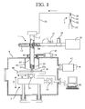
- Fig. 1 is an outline constitution view showing a nanotopography removing apparatus for removing nanotopography of a surface of a silicon wafer.
- the nanotopography removing apparatus is provided with a plasma generator 1, a gas supply apparatus 3 and an X-Y drive mechanism 5.
- the plasma generator 1 is an apparatus for producing activated species gas G including neutral radicals by subjecting a gas of an alumina discharge tube to plasma formation and is constituted by a microwave oscillator 10 and a waveguide 11.
- the microwave oscillator 10 is a magnetron and can oscillate microwave M at predetermined frequency.
- the waveguide 11 is for propagating the microwave M oscillated by the microwave oscillator 10 and an alumina discharge tube 2 is inserted laterally into the waveguide 11.
- a reflecting plate (short plunger) 12 for forming a standing wave by reflecting the microwave M is attached to an inner portion of a left side end of the waveguide 11. Further, at middle of the waveguide 11, there are attached a stub tuner 13 for carrying out phase matching of the microwave M and an isolator 14 for bending the reflected microwave M directed to the microwave oscillator 10 in a direction of 90 degrees (direction of surface of Fig. 1).
- the alumina discharge tube 2 is a cylindrical member having a nozzle portion 20 at its lower end portion and is connected with a supply pipe 30 of the gas supply apparatus 3 at its upper end portion.
- the gas supply apparatus 3 is an apparatus for supplying gas to inside of the alumina discharge tube 2, is provided with a cylinder 31 of SF 6 (sulfur hexafluoride) gas and the cylinder 31 is connected to the supply pipe 30 via valves 32 and a flow rate controller 33.
- SF 6 sulfur hexafluoride
- the sulfur hexafluoride gas can constitute single gas in this way, mixture gas including sulfur hexafluoride gas can also be constituted by simultaneously supplying other gas to the supply pipe 30.
- gas is supplied from the supply apparatus 3 to the alumina discharge tube 2 and when the microwave M is oscillated from the microwave oscillator 10, plasma formation of gas is carried out at inside of the alumina discharge tube 2 and the activated species gas G produced by the plasma formation is injected from the nozzle portion 20.
- a silicon wafer W When a silicon wafer W is arranged on a wafer table 40 at inside of a chamber 4, the silicon wafer W is adsorbed by electrostatic force of the wafer table 40.
- the chamber 4 is attached with a vacuum pump 41 and inside of the chamber 4 can be vacuumed by the vacuum pump 41.
- a hole 42 is perforated at a central portion of a top face of the chamber 4 and the nozzle portion 20 of the alumina discharge 2 is externally inserted into the chamber 4 via the hole 42.
- an O-ring 43 is mounted between the hole 42 and the alumina discharge tube 2 to thereby maintain an interval between the hole 42 and the alumina discharge tube 2 in airtight.
- a duct 44 is provided at a surrounding of the nozzle portion 20 inserted into the hole 42 and by driving a vacuum pump 45, gases produced by reaction in etching can be exhausted to outside of the chamber 4.
- the X-Y drive mechanism 5 is arranged at inside of the chamber 4 and supports the wafer table 40 from its lower side.
- the X-Y drive mechanism 5 moves the wafer table 40 in a left and right direction of Fig. 1 by an X drive motor 50 thereof and by a Y drive motor 51 thereof, the wafer table 40 and the X drive motor 50 are integrally moved in a direction of top and bottom of a paper face of Fig. 1. That is, by the X-Y drive mechanism 5, the nozzle portion 20 can be moved in X-Y directions relative to the silicon wafer W.
- SF 6 gas in the cylinder 31 flows out to the supply pipe 30 and is supplied to the alumina discharge tube 2.
- a flow rate of SF 6 gas is adjusted by an opening degree of the valve 32.
- the microwave oscillator 10 is driven. Then, SF 6 gas is subjected to plasma formation by the microwave M and there is produced the activated species gas G including F (fluorine) radicals (neutral activated species) constituting neutral radicals. Thereby, the activated species gas G is guided to the nozzle portion 20 of the alumina discharge tube 2 and is injected from an opening 20a of the nozzle portion 20 toward a side of the silicon wafer W.
- F fluorine radicals
- the X-Y drive mechanism 5 is driven by a control computer 49 and the wafer table 40 adsorbed with the silicon wafer W is moved in X-Y directions.
- various loci can be selected in accordance with a way of distributing nanotopography. A description will be given later of the loci.
- a material on a surface of the silicon wafer chemically reacts with the activated species gas, produced gaseous substances flow out from the site along with the injected gas and therefore, a material is removed from the surface of the silicon wafer W thereby.
- a removed amount of the material is substantially proportional to a time period of being exposed to the activated species gas and therefore, the removing amount is controlled by controlling relative speed between the silicon wafer W and the nozzle portion 20.
- Fig. 2 is a graph showing a distribution of an amount (depth) of a silicon wafer material per unit time removed by the injected activated species gas, which is very similar to a Gaussian distribution and is referred to as an etching profile.
- an etching rate E is provided with a maximum value Emax on a center line of the nozzle portion 20 and the etching rate E is reduced as the location becomes remote from the center in a radius r direction.
- the characteristic of the nozzle is represented by using a width indicating the etching rate E having a value of a half of Emax, that is, a half value width d.
- a planarizing apparatus which is referred to as a local etching apparatus, having the half value width d of around 25 mm.
- Figs. 3(a) and 3(b) are diagrams representing unevenness of a surface of a silicon wafer in which Fig. 3(a) shows a surface of a silicon wafer before subjected to planarizing and Fig. 3(b) shows a surface thereof after subjected to planarizing.
- the surface of the silicon wafer is formed by unevenness comprising comparatively short wavelength components a and comparatively long wavelength components b.
- the planarizing is carried out by the planarizing apparatus by the conventional way, macroscopically, it seems that planarizing is carried out by removing the long wavelength components b, however, microscopically, as shown by Fig. 3(b), unevenness of the short wavelength components a' remain substantially as they are (although wave heights are lowered).
- planarizing is carried out an etching profile having a large half value width d and accordingly, the unevenness having long wavelengths can selectively be removed and accordingly, the planarizing is realized by removing much of the projected portions (refer to b').
- the selective planarizing is not carried out with regard to microscopic, that is, short wavelength components, wave bottoms are removed along with wave tops and therefore, with regard to the short wavelength components the unevenness components remain substantially as they are (refer to a').
- the invention has been carried out based on such knowledge and nanotopography is removed by adjusting the half value width d of the etching profile to be substantially equal to or smaller than the wavelength of the nanotopography (about a half) .
- the wavelength of the nanotopography falls in a range of 0.2 mm through 20 mm and accordingly, the half value width d of the etching profile is selected in a range of 0.1 mm through 20 mm according to the invention.
- the half value width d is selected in such a range, projected portions of nanotopography can selectively be worked and nanotopography which has been regarded as impossible to be removed conventionally, can be removed.
- the lower limit value 0.1 mm of the etching profile is prescribed since the shortest wavelength grasped as nanotopography is 0.2 mm and an etching profile smaller than the shortest wavelength cannot actually be produced. Further, upper limit value 20 mm is prescribed since the longest wavelength grasped as nanotopography is 20 mm.
- the nanotopography removing apparatus is previously attached with a discharge tube (for example, alumina discharge tube 2) having such a nozzle portion 20 and it is also possible to make the nozzle portion 20 separable from the alumina discharge tube 2 and interchangeable by itself or along with the duct 44.
- a discharge tube for example, alumina discharge tube 2
- Nanotopography differs by respective silicon wafer and nanotopography appears uniformly over an entire face thereof or appears segregatedly. Further, a density of the distribution varies.
- the nozzle is scanned similar to the conventional planarizing apparatus and scanning speed is controlled in accordance with unevenness. In this case, the conventional planarizing can simultaneously be carried out.
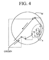
- Fig. 4 shows a resolution measure when a projected portion n of such a nanotopography is segregated and is a view showing an example of a locus when the nozzle is moved.
- the nozzle is moved at the fastest speed up to the area and at inside of the area, the nozzle is scanned by controlling the speed in accordance with degrees of unevenness.
- the X drive motor 50 and the Y drive motor 51 can also be driven by themselves respectively. In either of the cases, a distance and a time period of moving the nozzle can be made shorter than those in scanning the entire face of the wafer.
- Amounts (heights or wave heights), locations and distributions of unevenness of nanotopography have previously been measured by a measuring instrument (not illustrated) for respective semiconductor wafers and measurement data outputted from the measuring instrument is analyzed by the control computer 49. By the analysis, there are calculated necessary speed or scanning speed (amount removed by etching) , loci of the nozzle, nanotopography to be grouped and its area and the like.
- the method and the apparatus of the invention there is achieved an effect of capable of removing nanotopography which has already been produced on a surface of a semiconductor wafer which has been regarded as impossible to remove. Further, by constituting the half value width of etching profile of the activated species gas to be equal to or smaller than a wavelength of nanotopography and in a range equal to or larger than a half thereof, there is achieved an effect of capable of selectively removing projected portions of nanotopography.
Landscapes
- Physics & Mathematics (AREA)
- Engineering & Computer Science (AREA)
- Plasma & Fusion (AREA)
- Chemical & Material Sciences (AREA)
- Analytical Chemistry (AREA)
- Drying Of Semiconductors (AREA)
Applications Claiming Priority (2)
| Application Number | Priority Date | Filing Date | Title |
|---|---|---|---|
| JP2001027639A JP2002231700A (ja) | 2001-02-05 | 2001-02-05 | ナノトポグラフィ除去方法 |
| JP2001027639 | 2001-02-05 |
Publications (2)
| Publication Number | Publication Date |
|---|---|
| EP1229575A2 true EP1229575A2 (de) | 2002-08-07 |
| EP1229575A3 EP1229575A3 (de) | 2002-08-21 |
Family
ID=18892259
Family Applications (1)
| Application Number | Title | Priority Date | Filing Date |
|---|---|---|---|
| EP02001973A Withdrawn EP1229575A3 (de) | 2001-02-05 | 2002-02-04 | Verfahren zum Entfernen von Nanotopographie |
Country Status (3)
| Country | Link |
|---|---|
| US (1) | US6875701B2 (de) |
| EP (1) | EP1229575A3 (de) |
| JP (1) | JP2002231700A (de) |
Cited By (1)
| Publication number | Priority date | Publication date | Assignee | Title |
|---|---|---|---|---|
| EP1507172A1 (de) * | 2003-08-12 | 2005-02-16 | ASML Netherlands B.V. | Lithographischer Apparat und Verfahren zur Justierung des Apparats |
Families Citing this family (7)
| Publication number | Priority date | Publication date | Assignee | Title |
|---|---|---|---|---|
| JP3814558B2 (ja) | 2002-04-22 | 2006-08-30 | スピードファム株式会社 | 局所ドライエッチング方法及び半導体ウェハ表面の位置−厚さデータの処理方法 |
| KR100570122B1 (ko) * | 2003-05-12 | 2006-04-11 | 학교법인 한양학원 | 나노토포그라피 효과를 보상할 수 있는 화학기계적 연마용슬러리 조성물 및 이를 이용한 반도체소자의 표면 평탄화방법 |
| TWI323741B (en) * | 2004-12-16 | 2010-04-21 | K C Tech Co Ltd | Abrasive particles, polishing slurry, and producing method thereof |
| KR100641348B1 (ko) * | 2005-06-03 | 2006-11-03 | 주식회사 케이씨텍 | Cmp용 슬러리와 이의 제조 방법 및 기판의 연마 방법 |
| US8697576B2 (en) * | 2009-09-16 | 2014-04-15 | Cabot Microelectronics Corporation | Composition and method for polishing polysilicon |
| US8883034B2 (en) * | 2009-09-16 | 2014-11-11 | Brian Reiss | Composition and method for polishing bulk silicon |
| US8815110B2 (en) * | 2009-09-16 | 2014-08-26 | Cabot Microelectronics Corporation | Composition and method for polishing bulk silicon |
Family Cites Families (8)
| Publication number | Priority date | Publication date | Assignee | Title |
|---|---|---|---|---|
| US4734158A (en) * | 1987-03-16 | 1988-03-29 | Hughes Aircraft Company | Molecular beam etching system and method |
| US5254830A (en) * | 1991-05-07 | 1993-10-19 | Hughes Aircraft Company | System for removing material from semiconductor wafers using a contained plasma |
| JP2662321B2 (ja) * | 1991-05-31 | 1997-10-08 | 科学技術振興事業団 | 超低速クラスターイオンビームによる表面処理方法 |
| JPH0927482A (ja) | 1995-07-11 | 1997-01-28 | Speedfam Co Ltd | プラズマエッチング装置 |
| JP2000036488A (ja) * | 1998-07-21 | 2000-02-02 | Speedfam-Ipec Co Ltd | ウエハ平坦化方法及びそのシステム |
| US6147004A (en) * | 1998-07-21 | 2000-11-14 | Advanced Micro Devices, Inc. | Jet vapor reduction of the thickness of process layers |
| JP2002343772A (ja) * | 2001-05-18 | 2002-11-29 | Speedfam Co Ltd | 局所プラズマエッチング方法 |
| JP3814558B2 (ja) * | 2002-04-22 | 2006-08-30 | スピードファム株式会社 | 局所ドライエッチング方法及び半導体ウェハ表面の位置−厚さデータの処理方法 |
-
2001
- 2001-02-05 JP JP2001027639A patent/JP2002231700A/ja not_active Withdrawn
-
2002
- 2002-02-04 EP EP02001973A patent/EP1229575A3/de not_active Withdrawn
- 2002-02-05 US US10/062,494 patent/US6875701B2/en not_active Expired - Fee Related
Cited By (2)
| Publication number | Priority date | Publication date | Assignee | Title |
|---|---|---|---|---|
| EP1507172A1 (de) * | 2003-08-12 | 2005-02-16 | ASML Netherlands B.V. | Lithographischer Apparat und Verfahren zur Justierung des Apparats |
| US7078715B2 (en) | 2003-08-12 | 2006-07-18 | Asml Netherlands B.V. | Lithographic apparatus and apparatus adjustment method |
Also Published As
| Publication number | Publication date |
|---|---|
| US6875701B2 (en) | 2005-04-05 |
| US20020104825A1 (en) | 2002-08-08 |
| EP1229575A3 (de) | 2002-08-21 |
| JP2002231700A (ja) | 2002-08-16 |
Similar Documents
| Publication | Publication Date | Title |
|---|---|---|
| KR100617478B1 (ko) | 도포막 형성장치 및 도포막 형성방법 | |
| US5688415A (en) | Localized plasma assisted chemical etching through a mask | |
| US6875701B2 (en) | Nanotopography removing method | |
| KR101950068B1 (ko) | 임프린트 장치, 임프린트 방법 및 물품 제조 방법 | |
| US20050242062A1 (en) | Substrate processing method, substrate processing apparatus, and semiconductor device manufacturing method | |
| KR100710927B1 (ko) | 처리 방법 및 처리 시스템 | |
| KR100768580B1 (ko) | 식각 공정 툴에 의해 반도체 웨이퍼를 식각하는 방법 및 시스템과 이에 사용되는 프로그램 저장 장치 | |
| US6908566B2 (en) | Local dry etching method | |
| CN120473405A (zh) | 监测室漂移的方法 | |
| US20020144781A1 (en) | Local etching method | |
| JP2000124122A (ja) | 半導体露光装置および同装置を用いるデバイス製造方法 | |
| US6649528B2 (en) | Local dry etching method | |
| CN106062930A (zh) | 表面平坦化系统和方法 | |
| JP5652381B2 (ja) | 表面加工方法及び装置 | |
| US7094355B2 (en) | Local dry etching method | |
| JP5039939B2 (ja) | 表面加工方法及び装置 | |
| US20040063329A1 (en) | Multi-step local dry etching method for SOI wafer | |
| JP3950622B2 (ja) | ナノトポグラフィ評価用基準ウェーハとその製造方法 | |
| JP7012602B2 (ja) | 局所ドライエッチング装置 | |
| JP3486287B2 (ja) | プラズマエッチング装置 | |
| US7005032B2 (en) | Wafer table for local dry etching apparatus | |
| JP2024505843A (ja) | 自己組織化リソグラフィ | |
| KR20190094396A (ko) | 임프린트 장치, 및 물품의 제조 방법 | |
| JP3493261B2 (ja) | プラズマエッチング法及びプラズマエッチング装置 | |
| JP2001210626A (ja) | 半導体ウェーハの製造方法及び半導体ウェーハ |
Legal Events
| Date | Code | Title | Description |
|---|---|---|---|
| PUAI | Public reference made under article 153(3) epc to a published international application that has entered the european phase |
Free format text: ORIGINAL CODE: 0009012 |
|
| PUAL | Search report despatched |
Free format text: ORIGINAL CODE: 0009013 |
|
| AK | Designated contracting states |
Kind code of ref document: A2 Designated state(s): AT BE CH CY DE DK ES FI FR GB GR IE IT LI LU MC NL PT SE TR |
|
| AX | Request for extension of the european patent |
Free format text: AL;LT;LV;MK;RO;SI |
|
| AK | Designated contracting states |
Kind code of ref document: A3 Designated state(s): AT BE CH CY DE DK ES FI FR GB GR IE IT LI LU MC NL PT SE TR |
|
| AX | Request for extension of the european patent |
Free format text: AL;LT;LV;MK;RO;SI |
|
| 17P | Request for examination filed |
Effective date: 20020910 |
|
| 17Q | First examination report despatched |
Effective date: 20021203 |
|
| AKX | Designation fees paid |
Designated state(s): DE FR GB |
|
| 17Q | First examination report despatched |
Effective date: 20021203 |
|
| STAA | Information on the status of an ep patent application or granted ep patent |
Free format text: STATUS: THE APPLICATION IS DEEMED TO BE WITHDRAWN |
|
| 18D | Application deemed to be withdrawn |
Effective date: 20070301 |