EP1233447A2 - Halbleiterbauelement - Google Patents
Halbleiterbauelement Download PDFInfo
- Publication number
- EP1233447A2 EP1233447A2 EP01120671A EP01120671A EP1233447A2 EP 1233447 A2 EP1233447 A2 EP 1233447A2 EP 01120671 A EP01120671 A EP 01120671A EP 01120671 A EP01120671 A EP 01120671A EP 1233447 A2 EP1233447 A2 EP 1233447A2
- Authority
- EP
- European Patent Office
- Prior art keywords
- semiconductor device
- withstand voltage
- power semiconductor
- semiconductor elements
- elements
- Prior art date
- Legal status (The legal status is an assumption and is not a legal conclusion. Google has not performed a legal analysis and makes no representation as to the accuracy of the status listed.)
- Withdrawn
Links
Images


Classifications
-
- H—ELECTRICITY
- H10—SEMICONDUCTOR DEVICES; ELECTRIC SOLID-STATE DEVICES NOT OTHERWISE PROVIDED FOR
- H10D—INORGANIC ELECTRIC SEMICONDUCTOR DEVICES
- H10D86/00—Integrated devices formed in or on insulating or conducting substrates, e.g. formed in silicon-on-insulator [SOI] substrates or on stainless steel or glass substrates
- H10D86/01—Manufacture or treatment
-
- H—ELECTRICITY
- H10—SEMICONDUCTOR DEVICES; ELECTRIC SOLID-STATE DEVICES NOT OTHERWISE PROVIDED FOR
- H10W—GENERIC PACKAGES, INTERCONNECTIONS, CONNECTORS OR OTHER CONSTRUCTIONAL DETAILS OF DEVICES COVERED BY CLASS H10
- H10W10/00—Isolation regions in semiconductor bodies between components of integrated devices
- H10W10/01—Manufacture or treatment
- H10W10/011—Manufacture or treatment of isolation regions comprising dielectric materials
- H10W10/014—Manufacture or treatment of isolation regions comprising dielectric materials using trench refilling with dielectric materials, e.g. shallow trench isolations
- H10W10/0143—Manufacture or treatment of isolation regions comprising dielectric materials using trench refilling with dielectric materials, e.g. shallow trench isolations comprising concurrently refilling multiple trenches having different shapes or dimensions
-
- H—ELECTRICITY
- H10—SEMICONDUCTOR DEVICES; ELECTRIC SOLID-STATE DEVICES NOT OTHERWISE PROVIDED FOR
- H10W—GENERIC PACKAGES, INTERCONNECTIONS, CONNECTORS OR OTHER CONSTRUCTIONAL DETAILS OF DEVICES COVERED BY CLASS H10
- H10W10/00—Isolation regions in semiconductor bodies between components of integrated devices
- H10W10/10—Isolation regions comprising dielectric materials
- H10W10/17—Isolation regions comprising dielectric materials formed using trench refilling with dielectric materials, e.g. shallow trench isolations
Definitions
- the withstand voltage of a single transistor when withstand voltage of a single transistor (MOSFET) is 40V to 60V, the withstand voltage of a high withstand voltage driver that is formed by connecting two such transistors in series in multistage becomes about 80 V to 120V which is twice as high as that of the single transistor, and it is possible to secure the withstand voltage required for the injector driver.
- MOSFET single transistor
- the withstand voltage of a high withstand voltage driver that is formed by connecting two such transistors in series in multistage becomes about 80 V to 120V which is twice as high as that of the single transistor, and it is possible to secure the withstand voltage required for the injector driver.
- each channel 1a, 1b, 2a, 2b, 3a, 3b, 4a, 4b, 5a, 5b, 6a, 6b has withstand voltage of 40V in single.
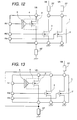
- the channel 1a, 2a, 3a, 4a, 5a, 6a is realized by a transistor 2 insulated by a trench 4 as in the embodiment shown in Fig. 1.
- a channel 7 to n is composed of an un-insulated transistor (MOSFET) as the transistor 3' shown in Fig. 10.
- channels 1 to 4 each have withstand voltage of 80V.
- methods of realizing the channels 1 to 4 there are a method of connecting in series the transistors 2 and 3 insulated by the trench 4 as in the embodiment in Fig. 1, a method of making a horizontal distance between a drain and a source in a horizontal type transistor (MOSFET), etc., and any method can be taken.
- the channels 5a, 5b, 6a, 6b each have 40 V independently.
- the channels 5a, 6a are realized by the transistor 2 insulated by the trench 4 as in the embodiment in Fig. 1.
- the channels 7-n each are constructed from a transistor(MOSFET) which is not insulated as in the transistor 3' in Fig. 10.
- the channels 1 to 4 of each LSI are used as injector drivers
- the channels 5a, 5b, 6a, 6b and the channels 7 to n are used as drivers of a low voltage load other than a usual solenoid, a heater, a relay, etc.
- the channels 5a, 5b, 6a, 6b can be used as a full bridge for driving a throttle motor as in Fig. 26.
- drivers of different withstand voltage are mixed and disposed on the same chip, in addition the same kind of LSI can be effectually used commonly to control for a 4 cylinder engine, 6 cylinder engine or 8 cylinder engine, so that it is possible to reduce a development cost and a production cost by a mass production effect.
- one channel of injector driver of a high withstand voltage is used as a low withstand voltage driver, it can be used for two channels, in addition, the on-resistance can be reduced to 1/2.
- the channels 1 to 4 of each LSI are used as igniter drivers, the channels 5a to 5j, 6a to 6j and the channels 7 to n are used as drivers of a low voltage load other than a usual solenoid, a heater, a relay, etc..
- the channels 5a to 5j, 6a to 6j can be used as a full bridge for driving a throttle motor as in Fig. 26.
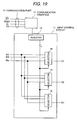
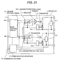
- the voltage between the drain and the source does not become large even if the transistor is turned off, it is possible to detect them by monitoring the voltage between the drain and the source. Further, at the time of the line breakage of load, the power supply fault and the ground fault, they are informed to a microprocessor, etc, out of the system through the communication interface 12 and the communication port 13.
- the linkage protection logic 19-1, 19-2 operate linkage protection on the basis of linkage control signals 21.
- the linkage protection is needed, that is, in the case where the transistors 2, 3 are being connected in series, over current is detected by any one of the current detecting means 18-1, 18-2, both of the transistors 2, 3 are turned off.
- the linkage protection is unnecessary, that is, in the case where the transistors 2, 3 are not connected in series, when over current is detected by the current detecting means 18-1, only the transistor 2 corresponding thereto is turned off, and when over current is detected by the current detecting means 18-2, only the transistor 3 corresponding thereto is turned off.
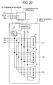
- Figs. 31, 32 examples in which it is applied to the driver LSI having an output port for one channel are shown for simplicity, however, it is possible to apply it to the driver LSI having output ports for plural channels. Particularly, as in the examples shown in Figs. 27 to 29, it is matter-of-course that it can be applied to the driver LSI having output ports for channels of the optimum number for construction of the engine controllers.
- the present invention it is possible to integrate a plurality of semiconductor drivers having different withstand voltage on the same chip, whereby it is possible to make small the size of apparatuses using power semiconductors and to reduce the cost.
Landscapes
- Metal-Oxide And Bipolar Metal-Oxide Semiconductor Integrated Circuits (AREA)
- Element Separation (AREA)
- Thin Film Transistor (AREA)
- Ignition Installations For Internal Combustion Engines (AREA)
- Electrical Control Of Air Or Fuel Supplied To Internal-Combustion Engine (AREA)
- Semiconductor Integrated Circuits (AREA)
Applications Claiming Priority (2)
| Application Number | Priority Date | Filing Date | Title |
|---|---|---|---|
| JP2001038685 | 2001-02-15 | ||
| JP2001038685A JP2002246551A (ja) | 2001-02-15 | 2001-02-15 | 半導体装置 |
Publications (2)
| Publication Number | Publication Date |
|---|---|
| EP1233447A2 true EP1233447A2 (de) | 2002-08-21 |
| EP1233447A3 EP1233447A3 (de) | 2005-01-19 |
Family
ID=18901611
Family Applications (1)
| Application Number | Title | Priority Date | Filing Date |
|---|---|---|---|
| EP20010120671 Withdrawn EP1233447A3 (de) | 2001-02-15 | 2001-08-31 | Halbleiterbauelement |
Country Status (3)
| Country | Link |
|---|---|
| US (2) | US6624474B2 (de) |
| EP (1) | EP1233447A3 (de) |
| JP (1) | JP2002246551A (de) |
Cited By (3)
| Publication number | Priority date | Publication date | Assignee | Title |
|---|---|---|---|---|
| EP1180800A3 (de) * | 2000-08-14 | 2007-05-23 | Hitachi, Ltd. | Integriertes Halbleiterschaltkreisbauelement und dessen Herstellungsverfahren |
| EP2930743A1 (de) * | 2014-04-11 | 2015-10-14 | Nxp B.V. | Halbleiterisolationsstruktur |
| EP2985450A4 (de) * | 2013-04-11 | 2017-01-25 | Denso Corporation | Zündungssteuerungsvorrichtung |
Families Citing this family (15)
| Publication number | Priority date | Publication date | Assignee | Title |
|---|---|---|---|---|
| JP2004228466A (ja) * | 2003-01-27 | 2004-08-12 | Renesas Technology Corp | 集積半導体装置およびその製造方法 |
| US7135751B2 (en) | 2003-07-25 | 2006-11-14 | Fuji Electric Device Technology Co., Ltd. | High breakdown voltage junction terminating structure |
| JP2006029287A (ja) * | 2004-07-21 | 2006-02-02 | Nikki Co Ltd | 燃料噴射弁駆動ユニット |
| JP2006029285A (ja) * | 2004-07-21 | 2006-02-02 | Nikki Co Ltd | 燃料噴射制御ユニット |
| US7196392B2 (en) | 2004-11-29 | 2007-03-27 | Taiwan Semiconductor Manufacturing Co., Ltd. | Semiconductor structure for isolating integrated circuits of various operation voltages |
| JP2008123642A (ja) * | 2006-11-15 | 2008-05-29 | Samsung Electronics Co Ltd | 負電位モニターパッド制御回路及びそれを備えた不揮発性メモリ |
| JP2008283827A (ja) * | 2007-05-14 | 2008-11-20 | Fuji Electric Device Technology Co Ltd | スイッチング電源 |
| JP5492518B2 (ja) * | 2009-10-02 | 2014-05-14 | 株式会社日立製作所 | 半導体駆動回路、及びそれを用いた半導体装置 |
| JP5855133B2 (ja) * | 2011-12-20 | 2016-02-09 | 三菱電機株式会社 | 充電装置 |
| US9049665B2 (en) * | 2011-12-22 | 2015-06-02 | Advantest Corporation | EMO linkage simplification |
| JP2013187488A (ja) * | 2012-03-09 | 2013-09-19 | Panasonic Corp | 半導体リレー装置 |
| JP6376253B2 (ja) * | 2013-04-11 | 2018-08-22 | 株式会社デンソー | 点火制御装置 |
| US11342288B2 (en) | 2019-06-04 | 2022-05-24 | Allegro Microsystems, Llc | Signal isolator having at least one isolation island |
| US11183452B1 (en) | 2020-08-12 | 2021-11-23 | Infineon Technologies Austria Ag | Transfering informations across a high voltage gap using capacitive coupling with DTI integrated in silicon technology |
| US11515246B2 (en) * | 2020-10-09 | 2022-11-29 | Allegro Microsystems, Llc | Dual circuit digital isolator |
Family Cites Families (13)
| Publication number | Priority date | Publication date | Assignee | Title |
|---|---|---|---|---|
| US5332920A (en) * | 1988-02-08 | 1994-07-26 | Kabushiki Kaisha Toshiba | Dielectrically isolated high and low voltage substrate regions |
| JPH073944B2 (ja) * | 1988-09-16 | 1995-01-18 | 富士電機株式会社 | 絶縁ゲート型半導体素子の駆動方法 |
| US5594379A (en) * | 1995-07-07 | 1997-01-14 | International Rectifier Corporation | Method and Circuit to eliminate false triggering of power devices in optically coupled drive circuits caused by dv/dt sensitivity of optocouplers |
| JPH09213956A (ja) * | 1996-02-07 | 1997-08-15 | Nec Kansai Ltd | 半導体装置及びその製造方法 |
| JP3575908B2 (ja) * | 1996-03-28 | 2004-10-13 | 株式会社東芝 | 半導体装置 |
| DE19626630C1 (de) * | 1996-07-02 | 1997-09-11 | Siemens Ag | Vorrichtung zum Schalten eines induktiven Verbrauchers |
| WO1998044687A1 (fr) * | 1997-03-31 | 1998-10-08 | Hitachi, Ltd. | Modem utilisant une barriere isolante capacitive et un coupleur insolant, et circuit integre utilise par ce modem |
| JPH11136293A (ja) | 1997-10-31 | 1999-05-21 | Hitachi Ltd | アイソレータ回路及びモノリシックアイソレータ |
| JPH11195712A (ja) * | 1997-11-05 | 1999-07-21 | Denso Corp | 半導体装置およびその製造方法 |
| JP4431208B2 (ja) | 1998-02-27 | 2010-03-10 | 株式会社日立製作所 | アイソレータ及びそれを用いるモデム装置 |
| JP3517154B2 (ja) * | 1998-04-30 | 2004-04-05 | 株式会社東芝 | 誘電体分離集積回路 |
| TW419810B (en) * | 1998-06-18 | 2001-01-21 | Hitachi Ltd | Semiconductor device |
| JP2001224138A (ja) * | 2000-02-07 | 2001-08-17 | Hitachi Ltd | 蓄電装置及び蓄電器の電圧検出方法 |
-
2001
- 2001-02-15 JP JP2001038685A patent/JP2002246551A/ja active Pending
- 2001-08-31 EP EP20010120671 patent/EP1233447A3/de not_active Withdrawn
- 2001-08-31 US US09/943,384 patent/US6624474B2/en not_active Expired - Fee Related
-
2003
- 2003-08-19 US US10/642,594 patent/US7161264B2/en not_active Expired - Fee Related
Cited By (6)
| Publication number | Priority date | Publication date | Assignee | Title |
|---|---|---|---|---|
| EP1180800A3 (de) * | 2000-08-14 | 2007-05-23 | Hitachi, Ltd. | Integriertes Halbleiterschaltkreisbauelement und dessen Herstellungsverfahren |
| EP2985450A4 (de) * | 2013-04-11 | 2017-01-25 | Denso Corporation | Zündungssteuerungsvorrichtung |
| US9765748B2 (en) | 2013-04-11 | 2017-09-19 | Denso Corporation | Ignition control apparatus |
| US10302062B2 (en) | 2013-04-11 | 2019-05-28 | Denso Corporation | Ignition control apparatus |
| EP2930743A1 (de) * | 2014-04-11 | 2015-10-14 | Nxp B.V. | Halbleiterisolationsstruktur |
| US9543288B2 (en) | 2014-04-11 | 2017-01-10 | Nxp B.V. | Semiconductor isolation structure |
Also Published As
| Publication number | Publication date |
|---|---|
| US6624474B2 (en) | 2003-09-23 |
| US7161264B2 (en) | 2007-01-09 |
| US20040051160A1 (en) | 2004-03-18 |
| EP1233447A3 (de) | 2005-01-19 |
| US20020109186A1 (en) | 2002-08-15 |
| JP2002246551A (ja) | 2002-08-30 |
Similar Documents
| Publication | Publication Date | Title |
|---|---|---|
| US6624474B2 (en) | Semiconductor device with scalable withstanding voltage | |
| EP2071724B1 (de) | Netzteilsteuerschaltung | |
| KR101385065B1 (ko) | 차지 펌프 회로 및 그 방법 | |
| US5723916A (en) | Electrical load driving device including load current limiting circuitry | |
| US20090243764A1 (en) | Gate-driver IC with HV-isolation, especially hybrid electric vehicle motor drive concept | |
| JPH1127931A (ja) | 抵抗をブートストラップ・ダイオードに直列結合したモノリシック・ゲート・ドライバ・デバイス | |
| CN103715193A (zh) | 用于n衬底高侧开关的反向极性保护 | |
| JPH02122665A (ja) | 電源バッテリの極性の反転に対して自己保護されている集積回路 | |
| US5812006A (en) | Optimized power output clamping structure | |
| DE102012215837A1 (de) | Halbleitervorrichtung | |
| US5023539A (en) | Alternator voltage transient minimization method and apparatus | |
| EP0523800B1 (de) | Überspannungsgeschützter Halbleiterschalter | |
| US6531908B1 (en) | Power output stage for switching inductive loads with reduced radiation emission | |
| EP1137068A2 (de) | Leistungshalbleiterbauelement mit Schutzschaltkreis | |
| US6597550B1 (en) | High voltage integrated circuit with resistor connected between substrate and ground to limit current during negative voltage spike | |
| US8278890B2 (en) | Power supply circuit | |
| US5923210A (en) | High side driver circuit with diagnostic output | |
| EP0632501A1 (de) | Halbleiteranordnung mit einem Schutzmittel | |
| EP2991226A1 (de) | Elektromagnetische spule zum antrieb einer steuerungsvorrichtung | |
| CN114696288A (zh) | 半导体装置、电子设备、车辆 | |
| Sakamoto et al. | An intelligent power IC with reverse battery protection for fast-switching high-side solenoid drive | |
| EP1865592B1 (de) | Schaltnetzteil | |
| JP2023136451A (ja) | 半導体装置、電子機器、車両 | |
| US6650521B2 (en) | Voltage division method for protection against load dump conditions | |
| Matsushita et al. | A surge-free intelligent power device specific to automotive high side switches |
Legal Events
| Date | Code | Title | Description |
|---|---|---|---|
| PUAI | Public reference made under article 153(3) epc to a published international application that has entered the european phase |
Free format text: ORIGINAL CODE: 0009012 |
|
| AK | Designated contracting states |
Kind code of ref document: A2 Designated state(s): AT BE CH CY DE DK ES FI FR GB GR IE IT LI LU MC NL PT SE TR |
|
| AX | Request for extension of the european patent |
Free format text: AL;LT;LV;MK;RO;SI |
|
| PUAL | Search report despatched |
Free format text: ORIGINAL CODE: 0009013 |
|
| AK | Designated contracting states |
Kind code of ref document: A3 Designated state(s): AT BE CH CY DE DK ES FI FR GB GR IE IT LI LU MC NL PT SE TR |
|
| AX | Request for extension of the european patent |
Extension state: AL LT LV MK RO SI |
|
| 17P | Request for examination filed |
Effective date: 20050510 |
|
| AKX | Designation fees paid |
Designated state(s): DE FR GB IT |
|
| 17Q | First examination report despatched |
Effective date: 20060317 |
|
| 17Q | First examination report despatched |
Effective date: 20060317 |
|
| GRAP | Despatch of communication of intention to grant a patent |
Free format text: ORIGINAL CODE: EPIDOSNIGR1 |
|
| STAA | Information on the status of an ep patent application or granted ep patent |
Free format text: STATUS: THE APPLICATION IS DEEMED TO BE WITHDRAWN |
|
| 18D | Application deemed to be withdrawn |
Effective date: 20090806 |