EP1233462A2 - Actionneur multicouche avec zones déplacées de contact des électrodes intérieures ayant la même polarisation que leur électrode extérieur - Google Patents
Actionneur multicouche avec zones déplacées de contact des électrodes intérieures ayant la même polarisation que leur électrode extérieur Download PDFInfo
- Publication number
- EP1233462A2 EP1233462A2 EP02003090A EP02003090A EP1233462A2 EP 1233462 A2 EP1233462 A2 EP 1233462A2 EP 02003090 A EP02003090 A EP 02003090A EP 02003090 A EP02003090 A EP 02003090A EP 1233462 A2 EP1233462 A2 EP 1233462A2
- Authority
- EP
- European Patent Office
- Prior art keywords
- actuator according
- piezoceramic
- electrodes
- offset
- electrode
- Prior art date
- Legal status (The legal status is an assumption and is not a legal conclusion. Google has not performed a legal analysis and makes no representation as to the accuracy of the status listed.)
- Granted
Links
- 230000010287 polarization Effects 0.000 title 1
- 238000004519 manufacturing process Methods 0.000 claims description 6
- 239000000463 material Substances 0.000 claims description 6
- 238000005245 sintering Methods 0.000 claims description 5
- 238000007493 shaping process Methods 0.000 claims description 3
- 238000002347 injection Methods 0.000 claims description 2
- 239000007924 injection Substances 0.000 claims description 2
- 238000005336 cracking Methods 0.000 abstract description 2
- 239000011888 foil Substances 0.000 description 7
- 239000011149 active material Substances 0.000 description 3
- 238000000034 method Methods 0.000 description 3
- 230000015572 biosynthetic process Effects 0.000 description 2
- 230000000694 effects Effects 0.000 description 2
- 230000005684 electric field Effects 0.000 description 2
- 229910052451 lead zirconate titanate Inorganic materials 0.000 description 2
- 238000007650 screen-printing Methods 0.000 description 2
- 230000007704 transition Effects 0.000 description 2
- 229910001374 Invar Inorganic materials 0.000 description 1
- 238000009825 accumulation Methods 0.000 description 1
- 230000015556 catabolic process Effects 0.000 description 1
- 239000000919 ceramic Substances 0.000 description 1
- 238000002485 combustion reaction Methods 0.000 description 1
- 238000006731 degradation reaction Methods 0.000 description 1
- 230000001419 dependent effect Effects 0.000 description 1
- 238000005516 engineering process Methods 0.000 description 1
- 238000000227 grinding Methods 0.000 description 1
- 238000009413 insulation Methods 0.000 description 1
- HFGPZNIAWCZYJU-UHFFFAOYSA-N lead zirconate titanate Chemical compound [O-2].[O-2].[O-2].[O-2].[O-2].[Ti+4].[Zr+4].[Pb+2] HFGPZNIAWCZYJU-UHFFFAOYSA-N 0.000 description 1
- 238000001465 metallisation Methods 0.000 description 1
- XLYOFNOQVPJJNP-UHFFFAOYSA-N water Substances O XLYOFNOQVPJJNP-UHFFFAOYSA-N 0.000 description 1
Images


Classifications
-
- H—ELECTRICITY
- H10—SEMICONDUCTOR DEVICES; ELECTRIC SOLID-STATE DEVICES NOT OTHERWISE PROVIDED FOR
- H10N—ELECTRIC SOLID-STATE DEVICES NOT OTHERWISE PROVIDED FOR
- H10N30/00—Piezoelectric or electrostrictive devices
- H10N30/80—Constructional details
- H10N30/87—Electrodes or interconnections, e.g. leads or terminals
- H10N30/871—Single-layered electrodes of multilayer piezoelectric or electrostrictive devices, e.g. internal electrodes
-
- H—ELECTRICITY
- H10—SEMICONDUCTOR DEVICES; ELECTRIC SOLID-STATE DEVICES NOT OTHERWISE PROVIDED FOR
- H10N—ELECTRIC SOLID-STATE DEVICES NOT OTHERWISE PROVIDED FOR
- H10N30/00—Piezoelectric or electrostrictive devices
- H10N30/50—Piezoelectric or electrostrictive devices having a stacked or multilayer structure
- H10N30/508—Piezoelectric or electrostrictive devices having a stacked or multilayer structure adapted for alleviating internal stress, e.g. cracking control layers
-
- H—ELECTRICITY
- H10—SEMICONDUCTOR DEVICES; ELECTRIC SOLID-STATE DEVICES NOT OTHERWISE PROVIDED FOR
- H10N—ELECTRIC SOLID-STATE DEVICES NOT OTHERWISE PROVIDED FOR
- H10N30/00—Piezoelectric or electrostrictive devices
- H10N30/01—Manufacture or treatment
- H10N30/05—Manufacture of multilayered piezoelectric or electrostrictive devices, or parts thereof, e.g. by stacking piezoelectric bodies and electrodes
- H10N30/053—Manufacture of multilayered piezoelectric or electrostrictive devices, or parts thereof, e.g. by stacking piezoelectric bodies and electrodes by integrally sintering piezoelectric or electrostrictive bodies and electrodes
-
- H—ELECTRICITY
- H10—SEMICONDUCTOR DEVICES; ELECTRIC SOLID-STATE DEVICES NOT OTHERWISE PROVIDED FOR
- H10N—ELECTRIC SOLID-STATE DEVICES NOT OTHERWISE PROVIDED FOR
- H10N30/00—Piezoelectric or electrostrictive devices
- H10N30/50—Piezoelectric or electrostrictive devices having a stacked or multilayer structure
- H10N30/503—Piezoelectric or electrostrictive devices having a stacked or multilayer structure having a non-rectangular cross-section in a plane orthogonal to the stacking direction, e.g. polygonal or circular in top view
- H10N30/505—Piezoelectric or electrostrictive devices having a stacked or multilayer structure having a non-rectangular cross-section in a plane orthogonal to the stacking direction, e.g. polygonal or circular in top view the cross-section being annular
Definitions
- the invention relates to a piezoceramic multilayer actuator according to the Preamble of the first claim and a method for its production.
- FIG. 1 shows a piezoceramic multi-layer actuator 1 according to the prior art shown schematically.
- These actuators have an interdigital structure. you will be manufactured as monoliths, that is, they consist of stacked thin layers 2 piezoelectrically active material, for example lead zirconate titanate (PZT), with interposed conductive inner electrodes 7, which alternately to the Actuator surface are performed.
- the active material is called a green film provided with internal electrodes 7 before sintering by a screen printing process pressed into a stack, pyrolyzed and then sintered, creating a monolithic Multi-layer actuator 1 is created.
- External electrodes 3, 4 connect the internal electrodes 7
- Inner electrodes 7 are electrically connected in parallel on one side of the actuator 1 and so grouped together.
- the outer electrodes 3, 4 are Connection poles of the actuator. An electrical voltage is applied via the connections 5 the connection poles are placed, so this is transmitted to all internal electrodes 7 in parallel and creates an electric field in all layers of the active material that is thereby mechanically deformed. The sum of all these mechanical deformations is available at the end faces of the actuator as usable expansion 6 and / or force Available, for example to control an injection valve Internal combustion engines.
- the cracks 8 are usually spaced apart by more than one millimeter Strains of about 1 to 2 ⁇ m / mm. These cracks 8 end in the so-called active Area of the actuator that generates the stretch, because here only compressive stresses occur.
- the cracks can be tolerated for some applications. However, it does result basic problems. If the actuator is not completely encapsulated, contact the through the cracks exposed electrode ends electrical fields that lead to Accumulation of water or polar molecules can lead. Cause this Leakage currents or lead to an increased degradation of the actuator behavior. It is also does not completely rule out that the actuators, through the cracks previously damaged, fail due to breakouts during operation. Farther the outer electrodes in the area of the cracks are particularly stressed and tear or come off. Failure of the outer electrode leads to total failure an actuator.
- the object of the invention is to determine the causes of the occurrence of crack-forming Eliminate tensions as far as possible.
- the task is solved with the help of the characteristic Characteristics of the first, according to the procedure with the help of the seventeenth claim.
- Advantageous embodiments of the invention are set out in the dependent claims claimed.
- a multilayer actuator according to the invention differs from actuators according to the State of the art in that the ones to be contacted with their outer electrode Surfaces of the same polarity of internal electrodes should not be stacked in a straight direction lie.
- the inner electrodes of the multilayer actuator according to the invention have one tongue-shaped, outward-facing from its base Contact area. The end faces of these contact areas are the contact areas. Only these contact areas reach the surface of the actuator and are on the respective outer electrode for connecting the equally polarized inner electrodes connected.
- the described shape of the internal electrodes results in tongue-shaped contact area an inactive area with a predefinable width.
- the Contact areas and thus the inactive areas assigned to them predetermined number of the same polarity, arranged one above the other in the same direction Internal electrodes are opposite the contact surfaces and thus the latter assigned inactive areas of the previous inner electrode or one predefined number of identical previous internal electrodes of the same type Polarity offset by a predetermined angle ⁇ . This creates inactive areas that are passively stretched.
- the offset should be a multiple of the angle ⁇ be so large that at least the contact areas of the first and the last of the no longer overlap the same electrodes in this area. Thereby the critical distance in which cracks form is overcome.
- Such an offset a given height can, depending on its size, can be provided several times in succession and can already occur approximately every 0.5 mm should be completed, but depending on the actuator size, should be updated at the latest about 3 mm should be completed, so that the effect of the stress relief occurs can.
- An advantageous range is approximately between 1 mm and 1.5 mm.
- the thickness of a layer is the thickness of the piezoceramic layer and the thickness the inner electrode is usually 100 ⁇ m, that is 0.1 mm.
- the range to be regarded as advantageous is approximately between 10 and 15 layers.
- the offset to remove the coverage of the contact areas and the inactive Areas can be made so that each layer faces the subsequent layer offset with a similarly polarized inner electrode by a predetermined angle is arranged. However, two or more layers with the same polarity can also be used Internal electrodes are first placed one above the other in the same arrangement before Offset by a predetermined angle.
- the actuators can have a circular cross section.
- the cross-sectional area can also be a square, a rectangle or a polygon.
- the cross-section and the constant offset have an outer electrode helical course.
- a Outer electrode over one or, in particular with a polygonal cross section run over several side surfaces.
- the multi-layer actuators can be fastened in their longitudinal axis for fastening have through hole, it is advantageous to in before sintering to bring in the soft green body.
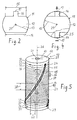
- FIG. 2 shows the design of an inner electrode 11 according to the invention.
- the circular cross-sectional area 12 with the radius (R) 13 is on one side cut off a circular section with a secant 14 of length L.
- On the opposite side is of the same size circular section with the same long secant 15 a demarcated from the remaining base 12 tongue-shaped, outwardly facing contact area 16 remained. Since the Inner electrode 11 has a certain thickness, is the secant of the contact area 16 with the width b the edge of the contact surface 17 for connection to the Outer electrode.
- FIG. 3 shows three green foils 18, 19, 20.
- the assignment of a green sheet with several Internal electrodes enable the rational production of multiple multilayer actuators simultaneously.
- the required number of foils are stacked on top of one another that the inner electrodes are on top of each other, and then, because of the light weight Separability if possible still in the green state, around the inner electrodes separated from each other. Then, also in the green state, the Finishing of the multi-layer actuators up to the specified green diameter of the multi-layer actuator.
- the arrangement of the internal electrodes 11 on the respective green sheet 18, 19 or 20 is always in the same orientation.
- an offset occurs in the subsequent film Alignment of the inner electrodes, that is to say a rotation about their center point 21 a predetermined angle 22 of size ⁇ .
- the three green foils 18, 19 and 20 show so internal electrodes of the same polarity.
- the inner electrodes of opposite polarity can be in the same way getting produced. However, their orientation is opposite the orientation of the assigned internal electrode of opposite polarity, i.e. on the second, fourth and sixth films, each rotated by 180 degrees.
- the electrode layers with different polarity alternate.
- An arrangement of the top shows the oppositely polarized inner electrodes of successive foils to a section through the multilayer actuator 10 in Figure 4.
- the contact surface 17 of the The positive pole lies opposite the contact surface 17 of the negative pole rotated by 180 degrees, separated from each other by the ceramic film 25.
- the contact surfaces 17 (b) should no longer overlap after a predetermined height h (38 in FIG. 5), so that crack formation in the inactive areas is avoided.
- the effect is optimized if, after the critical distance h, the inactive areas of the first and last layer of film no longer overlap.
- the angle 22 of the size ⁇ , by which an inner electrode must be rotated with the same polarity with respect to the subsequent electrode, is calculated as follows for a given height h: where d (23 in FIG. 5) is the total thickness of the piezoceramic layer, the green film 25, and the thickness of the electrode layer 11 and R is the radius 13 of the multilayer actuator.
- the films are laminated after stacking one on top of the other, with a stack of films, a Block, which can comprise several multilayer actuators.
- a Block which can comprise several multilayer actuators.
- the actuators are, for example, by means of a Separator divided into six individual, rectangular cuboids. Each of the cuboids then corresponds to an actuator.
- the cuboids are so green on the desired diameter turned that next to the surfaces to be contacted inactive areas for insulation on the surface arise.
- the Actuators sintered, the desired one due to the homogeneous sintering shrinkage Gauge is reached. In the sintered state, the ends become plane-parallel ground.
- the contact surfaces 17 for connecting the outer electrode 24, by grinding be exposed.
- the contact surfaces 17 are provided with a basic metallization and then an electrode made of a suitable material, for example a sieve electrode from Invar, the course of the connection surfaces soldered following.
- the Electrode layer even from a conductive layer without additional Outside electrode exist.
- FIG. 5 shows a schematic, greatly enlarged representation Multi-layer actuator 10 according to the invention with a circular cross section and helical outer electrodes 24. While the The outer electrode is almost completely visible on the front, is the course of the Outer electrode, the oppositely polarized inner electrodes 11 with each other connects, not to be seen and therefore drawn in dashed lines.
- Centric to Longitudinal axis 26 runs through a bore 27 for fastening the actuator.
- the head area 28 and in foot area 29 is the transition to the inactive area with respect to occurring voltages designed uniformly by increasing the Distances of the inner electrodes to the respective end reduced the operating field strength becomes.
- the distance between the electrodes 30, 31, 32, and 33 on the head 28 increases from electrode to electrode towards the end of the actuator.
- Foot area 29 the distance between the electrodes 34, 35, 36 and 37.
- the remaining inner electrodes 11 are all the same distance apart.
- the through the outer electrodes 24 interconnected contact surfaces and thus the inactive areas 15 are continuously at the same angle to one another added.
- the critical distance 38 (h), according to that in the present exemplary embodiment the offset 41 is so large that no overlap of the inactive regions 15 is the same polarized electrodes 11 is more, is after six electrode layers or layers 23 reached, as can be counted between the electrodes 39 and 40.
Landscapes
- Engineering & Computer Science (AREA)
- Manufacturing & Machinery (AREA)
- Fuel-Injection Apparatus (AREA)
- General Electrical Machinery Utilizing Piezoelectricity, Electrostriction Or Magnetostriction (AREA)
- Micromachines (AREA)
- Fluid-Pressure Circuits (AREA)
Applications Claiming Priority (4)
| Application Number | Priority Date | Filing Date | Title |
|---|---|---|---|
| DE10107505 | 2001-02-15 | ||
| DE10107505 | 2001-02-15 | ||
| DE10201943A DE10201943A1 (de) | 2001-02-15 | 2002-01-19 | Vielschichtaktor mit versetzt angeordneten Kontaktflächen gleich gepolter Innenelektroden für ihre Außenelektrode |
| DE10201943 | 2002-01-19 |
Publications (3)
| Publication Number | Publication Date |
|---|---|
| EP1233462A2 true EP1233462A2 (fr) | 2002-08-21 |
| EP1233462A3 EP1233462A3 (fr) | 2005-07-27 |
| EP1233462B1 EP1233462B1 (fr) | 2007-07-18 |
Family
ID=26008536
Family Applications (1)
| Application Number | Title | Priority Date | Filing Date |
|---|---|---|---|
| EP02003090A Expired - Lifetime EP1233462B1 (fr) | 2001-02-15 | 2002-02-13 | Actionneur multicouche avec zones déplacées de contact des électrodes intérieures ayant la même polarisation que leur électrode extérieur |
Country Status (5)
| Country | Link |
|---|---|
| US (1) | US6922005B2 (fr) |
| EP (1) | EP1233462B1 (fr) |
| JP (1) | JP2002319716A (fr) |
| AT (1) | ATE367653T1 (fr) |
| DE (2) | DE10201943A1 (fr) |
Cited By (3)
| Publication number | Priority date | Publication date | Assignee | Title |
|---|---|---|---|---|
| EP1235285A3 (fr) * | 2001-02-21 | 2005-05-25 | CeramTec AG Innovative Ceramic Engineering | Méthode de fabrication des actionneurs piézocéramiques multicouche |
| WO2008040688A1 (fr) * | 2006-10-02 | 2008-04-10 | Robert Bosch Gmbh | Actionneur piézoélectrique, constitué d'éléments piézoélectriques empilés les uns sur les autres et électriquement connectés |
| EP2043171A3 (fr) * | 2007-09-27 | 2010-01-27 | Robert Bosch GmbH | Module de piézoactionneur comprenant plusieurs piézoactionneurs reliés ensembles et son procédé de fabrication |
Families Citing this family (5)
| Publication number | Priority date | Publication date | Assignee | Title |
|---|---|---|---|---|
| JP2006041281A (ja) * | 2004-07-28 | 2006-02-09 | Kyocera Corp | 積層型圧電素子およびこれを用いた噴射装置 |
| CN100563039C (zh) * | 2004-03-09 | 2009-11-25 | 京瓷株式会社 | 叠层型压电元件及其制造方法 |
| US7481642B2 (en) * | 2004-04-23 | 2009-01-27 | Husky Injection Molding Systems Ltd. | Method and apparatus for controlling a vent gap with active material elements |
| DE102004050803A1 (de) * | 2004-10-19 | 2006-04-20 | Robert Bosch Gmbh | Piezoaktor |
| JP5969863B2 (ja) * | 2012-08-30 | 2016-08-17 | 京セラ株式会社 | 圧電素子、音響発生器、音響発生装置及び電子機器 |
Family Cites Families (14)
| Publication number | Priority date | Publication date | Assignee | Title |
|---|---|---|---|---|
| JPS6086880A (ja) * | 1983-10-19 | 1985-05-16 | Nec Corp | 電歪効果素子 |
| US4803763A (en) * | 1986-08-28 | 1989-02-14 | Nippon Soken, Inc. | Method of making a laminated piezoelectric transducer |
| JPS63155684A (ja) * | 1986-12-18 | 1988-06-28 | Nippon Soken Inc | 積層型圧電体及びその製造方法 |
| JPH0228977A (ja) * | 1988-07-19 | 1990-01-31 | Toyota Motor Corp | 積層型圧電素子 |
| JPH02203579A (ja) * | 1989-02-01 | 1990-08-13 | Hitachi Metals Ltd | 積層型変位素子 |
| US5168189A (en) * | 1991-09-18 | 1992-12-01 | Caterpillar Inc. | Solderless connector for a solid state motor stack |
| EP0550829A1 (fr) * | 1991-12-05 | 1993-07-14 | Hoechst CeramTec Aktiengesellschaft | Procédé de fabrication de corps multicouche monolithiques pour des organes d'actionnement en céramique ferroélectrique |
| JP3137494B2 (ja) * | 1993-04-22 | 2001-02-19 | 三菱電機株式会社 | 電界発光素子およびこれを用いた表示装置 |
| JPH08167746A (ja) * | 1994-12-14 | 1996-06-25 | Kyocera Corp | 積層型圧電アクチュエータ |
| JPH09148639A (ja) * | 1995-11-24 | 1997-06-06 | Kyocera Corp | 積層型圧電アクチュエータ |
| JPH09148640A (ja) * | 1995-11-28 | 1997-06-06 | Tokin Corp | 積層型圧電アクチュエータ |
| DE19715488C1 (de) * | 1997-04-14 | 1998-06-25 | Siemens Ag | Piezoaktor mit neuer Kontaktierung und Herstellverfahren |
| DE19850610A1 (de) * | 1998-11-03 | 2000-05-04 | Bosch Gmbh Robert | Verfahren zur Herstellung piezoelektrischer Aktoren |
| EP1061591A4 (fr) * | 1998-12-18 | 2007-05-02 | Denso Corp | Corps multicouche piezoelectrique |
-
2002
- 2002-01-19 DE DE10201943A patent/DE10201943A1/de not_active Withdrawn
- 2002-02-13 DE DE50210476T patent/DE50210476D1/de not_active Expired - Lifetime
- 2002-02-13 AT AT02003090T patent/ATE367653T1/de not_active IP Right Cessation
- 2002-02-13 EP EP02003090A patent/EP1233462B1/fr not_active Expired - Lifetime
- 2002-02-14 US US10/076,227 patent/US6922005B2/en not_active Expired - Fee Related
- 2002-02-15 JP JP2002038824A patent/JP2002319716A/ja active Pending
Cited By (3)
| Publication number | Priority date | Publication date | Assignee | Title |
|---|---|---|---|---|
| EP1235285A3 (fr) * | 2001-02-21 | 2005-05-25 | CeramTec AG Innovative Ceramic Engineering | Méthode de fabrication des actionneurs piézocéramiques multicouche |
| WO2008040688A1 (fr) * | 2006-10-02 | 2008-04-10 | Robert Bosch Gmbh | Actionneur piézoélectrique, constitué d'éléments piézoélectriques empilés les uns sur les autres et électriquement connectés |
| EP2043171A3 (fr) * | 2007-09-27 | 2010-01-27 | Robert Bosch GmbH | Module de piézoactionneur comprenant plusieurs piézoactionneurs reliés ensembles et son procédé de fabrication |
Also Published As
| Publication number | Publication date |
|---|---|
| EP1233462A3 (fr) | 2005-07-27 |
| US20020195903A1 (en) | 2002-12-26 |
| DE50210476D1 (de) | 2007-08-30 |
| ATE367653T1 (de) | 2007-08-15 |
| EP1233462B1 (fr) | 2007-07-18 |
| DE10201943A1 (de) | 2002-10-24 |
| US6922005B2 (en) | 2005-07-26 |
| JP2002319716A (ja) | 2002-10-31 |
Similar Documents
| Publication | Publication Date | Title |
|---|---|---|
| EP1636859B1 (fr) | Element piezoelectrique avec un point de rupture prevu, methode de production de l'element, et utilisation de l'element | |
| EP1908131B1 (fr) | Procede de fabrication d'un actionneur piezoelectrique monolithique a sections d'empilement, actionneur piezoelectrique monolithique a sections d'empilement et utilisation dudit actionneur piezoelectrique | |
| EP1233461B1 (fr) | Actionneur multicouche piézocéramique avec une zone transitoire entre la zone active et la zone inactive de tête et de pied | |
| WO2006103154A1 (fr) | Composant piezo-electrique monolithique comportant une couche de decouplage mecanique, son procede de production et son utilisation | |
| DE19945933C1 (de) | Piezoaktor mit isolationszonenfreier elektrischer Kontaktierung und Verfahren zu dessen Herstellung | |
| DE102007016316A1 (de) | Verfahren und System zum Trennen einer Vielzahl von keramischen Bauelementen aus einem Bauelementeblock | |
| EP1233462B1 (fr) | Actionneur multicouche avec zones déplacées de contact des électrodes intérieures ayant la même polarisation que leur électrode extérieur | |
| EP2740163B1 (fr) | Empilement piézoélectrique entièrement actif à passivation | |
| EP1129493B1 (fr) | Structure multicouche piezoceramique presentant une surface de section polygonale | |
| EP2798679B1 (fr) | Pile piézo-électrique avec passivation et procédé de passivation d'une pile piézo-électrique | |
| DE10017975A1 (de) | Piezoelektrischer Vielschichtaktor | |
| DE102006001656A1 (de) | Piezoaktor und Verfahren zur Herstellung desselben | |
| DE10112588C1 (de) | Piezoaktor sowie Verfahren zur Herstellung eines Piezoaktors | |
| WO2001024286A1 (fr) | Actionneur piezo-electrique | |
| DE102005002980B3 (de) | Monolithischer Vielschichtaktor und Verfahren zu seiner Herstellung | |
| DE102005052686A1 (de) | Piezoaktor und Verfahren zur Herstellung desselben | |
| DE102005033463B3 (de) | Piezoaktor | |
| DE102005052714B4 (de) | Piezoaktor und Verfahren zur Herstellung desselben | |
| DE10121271A1 (de) | Grünkörper, piezoelektrisches Bauteil sowie Verfahren zum Herstellen eines piezoelektrischen Bauteils | |
| WO2005069393A1 (fr) | Piezo-actionneur et procede de fabrication dudit piezo-actionneur | |
| DE102005050340A1 (de) | Piezoaktor und Verfahren zur Herstellung desselben | |
| DE10257952A1 (de) | Piezoaktor und ein Verfahren zu dessen Herstellung | |
| WO2017028985A1 (fr) | Composant piézoélectrique | |
| DE102008031641B4 (de) | Piezoaktor in Vielschichtbauweise | |
| EP0817285A1 (fr) | Composite piézo-céramique multicouche |
Legal Events
| Date | Code | Title | Description |
|---|---|---|---|
| PUAI | Public reference made under article 153(3) epc to a published international application that has entered the european phase |
Free format text: ORIGINAL CODE: 0009012 |
|
| AK | Designated contracting states |
Kind code of ref document: A2 Designated state(s): AT BE CH CY DE DK ES FI FR GB GR IE IT LI LU MC NL PT SE TR |
|
| AX | Request for extension of the european patent |
Free format text: AL;LT;LV;MK;RO;SI |
|
| PUAL | Search report despatched |
Free format text: ORIGINAL CODE: 0009013 |
|
| AK | Designated contracting states |
Kind code of ref document: A3 Designated state(s): AT BE CH CY DE DK ES FI FR GB GR IE IT LI LU MC NL PT SE TR |
|
| AX | Request for extension of the european patent |
Extension state: AL LT LV MK RO SI |
|
| 17P | Request for examination filed |
Effective date: 20060127 |
|
| AKX | Designation fees paid |
Designated state(s): AT BE CH CY DE DK ES FI FR GB GR IE IT LI LU MC NL PT SE TR |
|
| GRAP | Despatch of communication of intention to grant a patent |
Free format text: ORIGINAL CODE: EPIDOSNIGR1 |
|
| GRAS | Grant fee paid |
Free format text: ORIGINAL CODE: EPIDOSNIGR3 |
|
| GRAA | (expected) grant |
Free format text: ORIGINAL CODE: 0009210 |
|
| AK | Designated contracting states |
Kind code of ref document: B1 Designated state(s): AT BE CH CY DE DK ES FI FR GB GR IE IT LI LU MC NL PT SE TR |
|
| REG | Reference to a national code |
Ref country code: GB Ref legal event code: FG4D Free format text: NOT ENGLISH |
|
| REG | Reference to a national code |
Ref country code: CH Ref legal event code: EP |
|
| REF | Corresponds to: |
Ref document number: 50210476 Country of ref document: DE Date of ref document: 20070830 Kind code of ref document: P |
|
| REG | Reference to a national code |
Ref country code: IE Ref legal event code: FG4D Free format text: LANGUAGE OF EP DOCUMENT: GERMAN |
|
| PG25 | Lapsed in a contracting state [announced via postgrant information from national office to epo] |
Ref country code: NL Free format text: LAPSE BECAUSE OF FAILURE TO SUBMIT A TRANSLATION OF THE DESCRIPTION OR TO PAY THE FEE WITHIN THE PRESCRIBED TIME-LIMIT Effective date: 20070718 Ref country code: ES Free format text: LAPSE BECAUSE OF FAILURE TO SUBMIT A TRANSLATION OF THE DESCRIPTION OR TO PAY THE FEE WITHIN THE PRESCRIBED TIME-LIMIT Effective date: 20071029 Ref country code: FI Free format text: LAPSE BECAUSE OF FAILURE TO SUBMIT A TRANSLATION OF THE DESCRIPTION OR TO PAY THE FEE WITHIN THE PRESCRIBED TIME-LIMIT Effective date: 20070718 Ref country code: PT Free format text: LAPSE BECAUSE OF FAILURE TO SUBMIT A TRANSLATION OF THE DESCRIPTION OR TO PAY THE FEE WITHIN THE PRESCRIBED TIME-LIMIT Effective date: 20071218 |
|
| NLV1 | Nl: lapsed or annulled due to failure to fulfill the requirements of art. 29p and 29m of the patents act | ||
| GBV | Gb: ep patent (uk) treated as always having been void in accordance with gb section 77(7)/1977 [no translation filed] |
Effective date: 20070718 |
|
| REG | Reference to a national code |
Ref country code: IE Ref legal event code: FD4D |
|
| EN | Fr: translation not filed | ||
| PG25 | Lapsed in a contracting state [announced via postgrant information from national office to epo] |
Ref country code: GR Free format text: LAPSE BECAUSE OF FAILURE TO SUBMIT A TRANSLATION OF THE DESCRIPTION OR TO PAY THE FEE WITHIN THE PRESCRIBED TIME-LIMIT Effective date: 20071019 Ref country code: DK Free format text: LAPSE BECAUSE OF FAILURE TO SUBMIT A TRANSLATION OF THE DESCRIPTION OR TO PAY THE FEE WITHIN THE PRESCRIBED TIME-LIMIT Effective date: 20070718 |
|
| PLBE | No opposition filed within time limit |
Free format text: ORIGINAL CODE: 0009261 |
|
| STAA | Information on the status of an ep patent application or granted ep patent |
Free format text: STATUS: NO OPPOSITION FILED WITHIN TIME LIMIT |
|
| PG25 | Lapsed in a contracting state [announced via postgrant information from national office to epo] |
Ref country code: IE Free format text: LAPSE BECAUSE OF FAILURE TO SUBMIT A TRANSLATION OF THE DESCRIPTION OR TO PAY THE FEE WITHIN THE PRESCRIBED TIME-LIMIT Effective date: 20070718 Ref country code: GB Free format text: LAPSE BECAUSE OF FAILURE TO SUBMIT A TRANSLATION OF THE DESCRIPTION OR TO PAY THE FEE WITHIN THE PRESCRIBED TIME-LIMIT Effective date: 20070718 |
|
| 26N | No opposition filed |
Effective date: 20080421 |
|
| PG25 | Lapsed in a contracting state [announced via postgrant information from national office to epo] |
Ref country code: SE Free format text: LAPSE BECAUSE OF FAILURE TO SUBMIT A TRANSLATION OF THE DESCRIPTION OR TO PAY THE FEE WITHIN THE PRESCRIBED TIME-LIMIT Effective date: 20071018 |
|
| PG25 | Lapsed in a contracting state [announced via postgrant information from national office to epo] |
Ref country code: FR Free format text: LAPSE BECAUSE OF FAILURE TO SUBMIT A TRANSLATION OF THE DESCRIPTION OR TO PAY THE FEE WITHIN THE PRESCRIBED TIME-LIMIT Effective date: 20080314 |
|
| BERE | Be: lapsed |
Owner name: CERAMTEC A.G. INNOVATIVE CERAMIC ENGINEERING Effective date: 20080228 |
|
| REG | Reference to a national code |
Ref country code: CH Ref legal event code: PL |
|
| PG25 | Lapsed in a contracting state [announced via postgrant information from national office to epo] |
Ref country code: CH Free format text: LAPSE BECAUSE OF NON-PAYMENT OF DUE FEES Effective date: 20080229 Ref country code: LI Free format text: LAPSE BECAUSE OF NON-PAYMENT OF DUE FEES Effective date: 20080229 Ref country code: MC Free format text: LAPSE BECAUSE OF NON-PAYMENT OF DUE FEES Effective date: 20080228 |
|
| PG25 | Lapsed in a contracting state [announced via postgrant information from national office to epo] |
Ref country code: BE Free format text: LAPSE BECAUSE OF NON-PAYMENT OF DUE FEES Effective date: 20080228 |
|
| PG25 | Lapsed in a contracting state [announced via postgrant information from national office to epo] |
Ref country code: AT Free format text: LAPSE BECAUSE OF NON-PAYMENT OF DUE FEES Effective date: 20080213 |
|
| PG25 | Lapsed in a contracting state [announced via postgrant information from national office to epo] |
Ref country code: CY Free format text: LAPSE BECAUSE OF FAILURE TO SUBMIT A TRANSLATION OF THE DESCRIPTION OR TO PAY THE FEE WITHIN THE PRESCRIBED TIME-LIMIT Effective date: 20070718 |
|
| PG25 | Lapsed in a contracting state [announced via postgrant information from national office to epo] |
Ref country code: LU Free format text: LAPSE BECAUSE OF NON-PAYMENT OF DUE FEES Effective date: 20080213 |
|
| PG25 | Lapsed in a contracting state [announced via postgrant information from national office to epo] |
Ref country code: TR Free format text: LAPSE BECAUSE OF FAILURE TO SUBMIT A TRANSLATION OF THE DESCRIPTION OR TO PAY THE FEE WITHIN THE PRESCRIBED TIME-LIMIT Effective date: 20070718 |
|
| PG25 | Lapsed in a contracting state [announced via postgrant information from national office to epo] |
Ref country code: IT Free format text: LAPSE BECAUSE OF NON-PAYMENT OF DUE FEES Effective date: 20080229 |
|
| REG | Reference to a national code |
Ref country code: DE Ref legal event code: R081 Ref document number: 50210476 Country of ref document: DE Owner name: CERAMTEC GMBH, DE Free format text: FORMER OWNER: CERAMTEC AG, 73207 PLOCHINGEN, DE Effective date: 20110216 |
|
| PGFP | Annual fee paid to national office [announced via postgrant information from national office to epo] |
Ref country code: DE Payment date: 20160428 Year of fee payment: 15 |
|
| REG | Reference to a national code |
Ref country code: DE Ref legal event code: R119 Ref document number: 50210476 Country of ref document: DE |
|
| PG25 | Lapsed in a contracting state [announced via postgrant information from national office to epo] |
Ref country code: DE Free format text: LAPSE BECAUSE OF NON-PAYMENT OF DUE FEES Effective date: 20170901 |