EP1233490A2 - Halbleiterlasermodul und Phaserverstärker und optisches Kommunikationssytem unter Verwendung desselben - Google Patents
Halbleiterlasermodul und Phaserverstärker und optisches Kommunikationssytem unter Verwendung desselben Download PDFInfo
- Publication number
- EP1233490A2 EP1233490A2 EP02001930A EP02001930A EP1233490A2 EP 1233490 A2 EP1233490 A2 EP 1233490A2 EP 02001930 A EP02001930 A EP 02001930A EP 02001930 A EP02001930 A EP 02001930A EP 1233490 A2 EP1233490 A2 EP 1233490A2
- Authority
- EP
- European Patent Office
- Prior art keywords
- semiconductor laser
- reflectivity
- laser device
- module
- optical
- Prior art date
- Legal status (The legal status is an assumption and is not a legal conclusion. Google has not performed a legal analysis and makes no representation as to the accuracy of the status listed.)
- Withdrawn
Links
Images


Classifications
-
- H—ELECTRICITY
- H01—ELECTRIC ELEMENTS
- H01S—DEVICES USING THE PROCESS OF LIGHT AMPLIFICATION BY STIMULATED EMISSION OF RADIATION [LASER] TO AMPLIFY OR GENERATE LIGHT; DEVICES USING STIMULATED EMISSION OF ELECTROMAGNETIC RADIATION IN WAVE RANGES OTHER THAN OPTICAL
- H01S5/00—Semiconductor lasers
- H01S5/10—Construction or shape of the optical resonator, e.g. extended or external cavity, coupled cavities, bent-guide, varying width, thickness or composition of the active region
- H01S5/14—External cavity lasers
- H01S5/146—External cavity lasers using a fiber as external cavity
-
- H—ELECTRICITY
- H01—ELECTRIC ELEMENTS
- H01S—DEVICES USING THE PROCESS OF LIGHT AMPLIFICATION BY STIMULATED EMISSION OF RADIATION [LASER] TO AMPLIFY OR GENERATE LIGHT; DEVICES USING STIMULATED EMISSION OF ELECTROMAGNETIC RADIATION IN WAVE RANGES OTHER THAN OPTICAL
- H01S5/00—Semiconductor lasers
- H01S5/02—Structural details or components not essential to laser action
- H01S5/022—Mountings; Housings
- H01S5/0225—Out-coupling of light
- H01S5/02251—Out-coupling of light using optical fibres
-
- H—ELECTRICITY
- H01—ELECTRIC ELEMENTS
- H01S—DEVICES USING THE PROCESS OF LIGHT AMPLIFICATION BY STIMULATED EMISSION OF RADIATION [LASER] TO AMPLIFY OR GENERATE LIGHT; DEVICES USING STIMULATED EMISSION OF ELECTROMAGNETIC RADIATION IN WAVE RANGES OTHER THAN OPTICAL
- H01S5/00—Semiconductor lasers
- H01S5/02—Structural details or components not essential to laser action
- H01S5/028—Coatings ; Treatment of the laser facets, e.g. etching, passivation layers or reflecting layers
- H01S5/0287—Facet reflectivity
-
- H—ELECTRICITY
- H01—ELECTRIC ELEMENTS
- H01S—DEVICES USING THE PROCESS OF LIGHT AMPLIFICATION BY STIMULATED EMISSION OF RADIATION [LASER] TO AMPLIFY OR GENERATE LIGHT; DEVICES USING STIMULATED EMISSION OF ELECTROMAGNETIC RADIATION IN WAVE RANGES OTHER THAN OPTICAL
- H01S5/00—Semiconductor lasers
- H01S5/10—Construction or shape of the optical resonator, e.g. extended or external cavity, coupled cavities, bent-guide, varying width, thickness or composition of the active region
- H01S5/1039—Details on the cavity length
-
- H—ELECTRICITY
- H01—ELECTRIC ELEMENTS
- H01S—DEVICES USING THE PROCESS OF LIGHT AMPLIFICATION BY STIMULATED EMISSION OF RADIATION [LASER] TO AMPLIFY OR GENERATE LIGHT; DEVICES USING STIMULATED EMISSION OF ELECTROMAGNETIC RADIATION IN WAVE RANGES OTHER THAN OPTICAL
- H01S5/00—Semiconductor lasers
- H01S5/20—Structure or shape of the semiconductor body to guide the optical wave ; Confining structures perpendicular to the optical axis, e.g. index or gain guiding, stripe geometry, broad area lasers, gain tailoring, transverse or lateral reflectors, special cladding structures, MQW barrier reflection layers
- H01S5/22—Structure or shape of the semiconductor body to guide the optical wave ; Confining structures perpendicular to the optical axis, e.g. index or gain guiding, stripe geometry, broad area lasers, gain tailoring, transverse or lateral reflectors, special cladding structures, MQW barrier reflection layers having a ridge or stripe structure
- H01S5/227—Buried mesa structure ; Striped active layer
Definitions
- the present invention relates to a semiconductor laser module designed as a pumping source for an optical communications system. More particularly, the invention relates to a complex cavity type semiconductor laser module which has a Fabry-Pérot semiconductor laser device optically coupled to an optical feedback part, such as a fiber Bragg grating (FBG), a dielectric multilayered filter or a distribution Bragg reflector (DBR).
- FBG fiber Bragg grating
- DBR distribution Bragg reflector
- This module is useful as a laser module which has a characteristic of emitting a pumping laser beam with a high optical output, a laser module which has a characteristic of emitting a pumping laser beam with an optical stability or a pumping source which has a suppressed occurrence of kinks and is used in, for example, a wavelength division multiplexing system that employs a Raman amplification system.
- Wavelength division multiplexing (WDM) communications systems have been developed as optical communications systems that transmit a plurality of signal lights.
- optical amplifiers are arranged at predetermined locations in an optical path and a laser module incorporating a Fabry-Pérot semiconductor laser device is connected to each optical amplifier.
- a pumping laser beam having a predetermined oscillation spectrum is input to each optical amplifier from the laser module, the optical signal that has been attenuated in the transmission through the upstream path is amplified and the optically amplified signal light is transmitted again to the downstream path.
- an Er-doped fiber amplifier (EDFA) is widely used as an optical amplifier in that system.
- the EDFA executes optical amplification of a stimulated emission type. That is, Er ions are excited by a pumping laser beam which is input from the laser module and a flat gain wavelength bandwidth defined at the energy level appears in the EDFA. The signal light of the wavelength that is included in the flat gain wavelength bandwidth is optically amplified.
- the practical gain wavelength bandwidth which is concerned with the optical amplification of signal light or the flat gain wavelength bandwidth is about 1530 to 1610 nm. That is, in case where optical signal amplified in the system is limited to the one whose wavelength lies within the aforementioned bandwidth.
- the Raman amplification system also has been known as an optical amplification system for signal light.
- This amplification system has a characteristic such that signal light having a wider bandwidth can be optically amplified as compared with the case of the EDFA. Therefore, there is a growing expectation of adapting the Raman amplification system to optical communications systems.
- the Raman amplification system is an optical amplification system which employs such a phenomenon that as a laser beam having an extremely high optical output (pumping laser beam) is input to an optical fiber, stimulated Raman scattering occurs in the optical fiber, giving a gain at a frequency smaller by 13 THz than the wavelength of the pumping laser beam (on the longer wavelength side by approximately 100 nm), and as signal light of a wavelength included in the wavelength bandwidth that provides the gain is input to the optical fiber in such a pumped state, the signal light is optically amplified.
- the Raman amplification system can be directly adapted to existing optical paths because the system can use an optical fiber (optical path) itself as an amplification medium without using a special optical fiber. That is, unlike the EDFA system, the Raman amplification system can reduce relay points in the entire optical paths. This can simplify the maintenance and control of the entire system and reduce the construction cost and maintenance cost of the entire system while improving the reliability of the entire system.
- the Raman amplification system can optically amplify signal light of an arbitrary wavelength bandwidth because the system can provide a gain at a frequency smaller by 13 THz than the wavelength of a pumping laser beam of an arbitrary wavelength by varying the wavelength of a pumping laser beam to be input to an optical fiber, i.e., by inputting the pumping laser beam to the optical fiber.
- the gain of an optical fiber has a certain wavelength distribution.
- the gain that is realized in the Raman amplification has a peak in the vicinity of the wavelength of 1530 nm and has an asymmetrical gain distribution with a margin of about 20 nm around the peak wavelength.
- the Raman amplification system multiplexes a plurality of pumping laser beams whose center wavelengths and optical outputs have been adjusted and inputs the multiplexed laser beam to an optical fiber.
- the gains of the individual pumping laser beams are made to continuously overlap one another on the long wavelength side of about 100 nm, thereby realizing a gain of a wide wavelength bandwidth on the whole.
- the obtained Raman gain is about 3 dB, which is too small to adequately realize optical amplification of signal light.
- the Raman amplification system is demanded to generally use a pumping laser beam with a high optical output of 200 mW or greater, preferably 300 mW or greater and more preferably 400 mW to 1 W, in order to acquire a gain which can ensure optical amplification of signal light.
- an optical output with the desired intensity is acquired by multiplexing laser beams from a plurality of laser modules and inputting the multiplexed laser beam to an optical fiber as a pumping laser beam.
- the forward pumping system makes the polarization dependency of Raman amplification stronger, however, the system requires that the pumping laser beam in use should reduce the polarization dependency of Raman amplification. This makes it necessary to perform depolarization on the pumping laser beam to thereby reduce the degree of polarization (DOP).
- DOP degree of polarization
- the ratio of the power of a laser beam from each laser module which lies in the pass band of the wavelength multiplexing coupler to the entire power should be equal to or greater than a predetermined value, specifically, for example, 90% or higher, and the ratio should be stable while the laser module is driven.
- the degree of the width of the oscillation spectrum is an important factor to fulfill the requirement.
- the width of the oscillation spectrum becomes too wide, the number of Fabry-Pérot modes present in the width of the oscillation spectrum becomes large, so that at the time of driving the laser module, the power distribution among the Fabry-Pérot modes varies to the level at which noise or a variation in gain cannot be neglected.
- the multiplexing loss at the time of multiplexing the wavelengths by the wavelength multiplexing coupler becomes large. If the width of the oscillation spectrum becomes too narrow, on the other hand, it becomes difficult to reduce the polarization dependency of the Raman gain and a kink occurs in the current v.s. optical output characteristic of the laser module, thus limiting the optical output of the laser module.
- the "width of the oscillation spectrum” mentioned here is a wavelength bandwidth that provides a spectral intensity lower by 3 dB than a peak value in the waveform of the pumping laser beam from the laser module.
- the width of the oscillation spectrum should be 3 nm or narrower, preferably 2 nm or narrower.
- the pumping laser beam is required to have smaller degree of polarization and the width of the oscillation spectrum of 3 nm or narrower. It is known that the degree of polarization of a multimode pumping laser beam which has at least three Fabry-Pérot modes, preferably four to five, in the width of the oscillation spectrum becomes smaller.
- the laser module that is used when the Raman amplification system is adapted to the WDM communications system should meet the requirement that the width of the oscillation spectrum is 3 nm or narrower and a multimode pumping laser beam which has at least three Fabry-Pérot modes in the width of the oscillation spectrum should be emitted.
- the use of a multimode pumping laser beam is advantageous in making it difficult to cause a reduction in the pumping efficiency based on the stimulated Brillouin scattering which occurs when a high optical output concentrates in a narrow wavelength bandwidth.
- the preferable spacing between the Fabry-Pérot modes of the pumping laser beam is said to be 0.1 nm or larger.
- module A a following semiconductor laser module (module A).
- the module A comprises:
- a preferred module A satisfies the relationships represented by the following expressions: 1000 ⁇ m ⁇ L ⁇ 3500 ⁇ m and 0.1% ⁇ R 1 + c 2 R 2 ⁇ 4%
- module B there is provided a following semiconductor laser module (module B).
- the module B comprises:
- module C there is provided a following semiconductor laser module (module C).
- the module C comprises:
- a preferred module C satisfies the relationships represented by the following expressions: 1000 ⁇ m ⁇ L ⁇ 3500 ⁇ m 0.1% ⁇ R 1 + c 2 R 2 ⁇ 4% and R 1 /R 2 ⁇ 0.8
- the optical feedback part may be designed to have a reflection bandwidth ⁇ (nm) meeting the following condition: 0.2 nm ⁇ ⁇ ⁇ 3 nm thus providing as a more suitable optical module.
- a fiber amplifier which uses one of the modules A, B and C as a pumping source and an optical communications system which has the fiber amplifier and one of the modules A, B and C.
- a Fabry-Pérot semiconductor laser device having a cavity length set to 1000 ⁇ m or greater could provide a high optical output if optimized by reducing the reflectivity of the front facet (output facet).
- the present inventors reached the conclusion that the aforementioned Fabry-Pérot semiconductor laser device with a long cavity length should be used as a laser device (light source) to be incorporated in the semiconductor laser module.
- the present inventors paid attention to a method of forming an optical coupling system of a complex cavity type by optically coupling the laser device and a fiber Bragg grating.
- This method has been known as a method of fixing the oscillation wavelength of a Fabry-Pérot semiconductor laser device.
- the oscillation spectrum of the laser device changes, resulting in a change in the center wavelength of the gain wavelength bandwidth to be obtained. Because the mirror loss characteristic is lower at the vicinity of the center wavelength of the reflection bandwidth of the fiber Bragg grating, however, the oscillation spectrum of the laser device is pulled into the vicinity of the center wavelength of the reflection bandwidth of the fiber Bragg grating (pull-in of the oscillation spectrum of the laser device) so that the wavelength bandwidth of the laser beam emitted from the optical coupling system or the pumping laser beam is fixed to the vicinity of the center wavelength of the reflection bandwidth of the fiber Bragg grating.
- the equations (1) and (2) are essential conditions for the complex cavity type optical coupling system to provide a high optical output.
- the equation (3) means the essential condition for pulling the oscillation spectrum of the laser device into the vicinity of the center wavelength of the reflection bandwidth of the optical feedback part.
- the equation (4) means the essential condition for suppressing the occurrence of a kink attributable to longitudinal mode hopping when the module is driven.
- the module A functions as a complex cavity type pumping source which emits a high optical output.
- the module B functions as a complex cavity type pumping source which ensures at least the wavelength stability while being able to emit a high optical output.
- the module C that satisfies the equations (1), (2) and (3) surely has both characteristics of providing a high optical output and an excellent wavelength stability, and is very useful as a pumping source of the Raman amplification system.
- Any of the modules A, B and C that fulfill the equation (4) demonstrates its own function mentioned above as well as the suppressed occurrence of a kink.
- Those modules can have any optical feedback part as long as the optical feedback part has a wavelength selectivity and shows a specific reflectivity with respect to a specific wavelength.
- the optical feedback part has a wavelength selectivity and shows a specific reflectivity with respect to a specific wavelength.
- a fiber Bragg grating, a dielectric multilayered filter and a distribution Bragg reflector (DBR) are available as the optical feedback part. Of those three, the fiber Bragg grating is suitable.
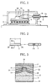
- the basic structure of the modules A, B and C of the present invention is exemplified in Fig. 1.
- the exemplified module uses a fiber Bragg grating as its optical feedback part.
- a package 1 houses a Peltier module 2 and a substrate 6 on which a Fabry-Pérot semiconductor laser device 3 with suppressed high-order transverse modes, as discussed later, a thermistor 4 and lenses 5a and 5b are secured is fixed on the Peltier module 2.
- An optical fiber 7 having a fiber Bragg grating 7A to be discussed later is secured into a through hole 1b formed in a side wall 1a of the package 1.
- each module as a laser beam which is emitted from a front facet 3A of the laser device 3 and has an oscillation spectrum formed by a plurality of Fabry-Pérot modes passes the two lenses 5a and 5b, the laser beam is condensed and input to the end face of the optical fiber 7.
- the laser beam is then waveguided through the core of the optical fiber 7 and of the waveguided laser beam, the Fabry-Pérot mode light that is included in the reflection bandwidth ( ⁇ ) of the fiber Bragg grating is reflected at the fiber Bragg grating 7A and returns to the laser device as a reflection light of a specific wavelength.
- Each module is of a complex cavity type in which resonance between the front facet 3A and a rear facet 3B of the laser device 3 and resonance between the rear facet 3B of the laser device 3 and the fiber Bragg grating 7A are compounded.
- the laser beam emitted from the laser device 3 carries out a sequence of resonant operations in which resonance in the cavity of the laser device 3 and resonance between the rear facet 3B and the fiber Bragg grating 7A are compounded, then becomes a high-power pumping laser beam and is transmitted to a predetermined place in the optical path from the optical fiber 7.
- each module of the present invention measures the device temperature with the thermistor 4 located near the laser device 3 and the laser device 3 is adequately cooled by regulating the operational current of the Peltier module 2 under the control of an external control circuit (not shown) using the measured value, so that the temperature of the laser device 3 is set constant.
- Any one of the modules can suppress the generation of a kink caused by longitudinal mode hopping by setting the reflection bandwidth ⁇ of the fiber Bragg grating to 3 nm or narrower.
- the optical coupling of the semiconductor laser device 3 and the fiber Bragg grating in the module in Fig. 1 from which the other components are omitted is illustrated as an exemplary diagram in Fig. 2.
- the optical fiber 7 having the fiber Bragg grating 7A formed therein is arranged facing the front facet 3A of the semiconductor laser device 3, thereby constituting the optical coupling system of the laser device 3 and the fiber Bragg grating 7A.
- the laser device 3 is the light emission source of the optical coupling system. If emission of a high optical output from the optical coupling system is achieved, it means that the laser device 3 as the light emission source provides a high optical output. In this respect, first it is necessary to look for a condition for realizing the emission of a high optical output from the laser device 3.
- the semiconductor laser device 3 in the optical coupling system is of a Fabry-Pérot type one example of which is depicted in Fig. 2 and a cross-sectional view of Fig. 3 along the line III-III in Fig. 2.
- the laser device 3 has a lower cladding layer 12, a lower GRIN-SCH layer 13, an active layer 14 with a quantum well structure and an upper GRIN-SCH layer 15 deposited in order on a substrate 11 of a predetermined semiconductor by a known epitaxial growth method, such as a metal organic vapor phase epitaxial growth method, liquid phase epitaxial method, molecular beam epitaxy, gas source molecular beam epitaxy or chemical beam epitaxy.
- An upper cladding layer 16 and a cap layer 17 are laminated on the upper GRIN-SCH layer 15.
- An upper electrode 18 is formed on the cap layer 17 and a lower electrode 19 is formed at the back of the substrate 11.
- a p-type layer 21 and an n-type layer 22 are laminated on the sides of the lower cladding layer 12, the lower GRIN-SCH layer 13, the active layer 14 and the upper GRIN-SCH layer 15 in the named order.
- the active layer 14 is surrounded by current blocking layer, thereby forming a realizing current ration and suppressing high order traverse modes.
- the laser device 3 is fabricated by forming a laminated structure of a semiconductor material by a predetermined epitaxial growth method, cleaving the structure to a predetermined cavity length L, depositing a low-reflectivity film on one cleaved face to form the front facet 3A having a peak reflectivity R 1 (%) and depositing a high-reflectivity film on the other cleaved face to form the rear facet 3B.
- the semiconductor material for the laser device 3 is adequately selected in consideration of the relation between the material property and the designated wavelength (center wavelength) of the pumping laser beam that is used in an optical amplifier for signal light.
- the laser device 3 can be fabricated by using a material selected from GaInAs, GaInAsP, AlGaInAs and GaInNAs material systems.
- the heat saturation phenomenon of the optical output is restrained and a variation in the center wavelength of the oscillation spectrum is restrained too. This makes it possible to increase the driving current of the laser device, thereby ensuring a high optical output as well as the stability of the center wavelength of the oscillation spectrum.
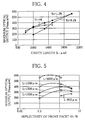
- the present inventors conducted the following experiment I and studied the relationship among the cavity length L, the peak reflectivity R 1 of the front facet and the optical output.
- the inventors fabricated various laser devices that have a layered structure shown in Fig. 3 or a lattice mismatched quantum well active region having both the lower GRIN-SCH layer 13 and the upper GRIN-SCH layer 15 formed of non-doped GaInAsP and having the active layer 14 formed of GaInAsP, by setting the reflectivity of the rear facet 3B constant to 95% and changing the cavity length L and the peak reflectivity R 1 of the front facet 3A.
- the laser devices were driven and the maximum optical outputs (Pmax: mW) of the laser devices were measured. The measuring results are illustrated in Figs. 4 and 5.
- the upper limit of the cavity length of the laser device 3 is set to 3500 ⁇ m.
- the cavity length L should be 1000 to 3500 ⁇ m, preferably be 3200 ⁇ m or shorter where the longitudinal mode spacing is 0.1 mm or longer, from the viewpoint of preventing stimulated Brillouin scattering.
- the reflectivity of the front facet should be set to 0.01 to 4%, preferably 0.1 to 4%.
- the module shown in Fig. 1 is a complex cavity type having the laser device 3 optically coupled to the fiber Bragg grating 7A. Unlike the laser device used in the experiment I which carries out resonance between one front facet and one rear facet, the module has resonance in the laser device 3 compounded with resonance between the fiber Bragg grating 7A and the rear facet 3B of the laser device 3, resulting in the emission of the pumping laser beam from the optical fiber 7.
- the module can be assumed as a laser device which has a single cavity structure.
- the reflectivity of the rear facet of the assumed laser device is equivalent to the reflectivity of the rear facet 3B of the actual laser device 3.
- the assumed laser device does not actually have a front facet. If the assumed laser device had the front facet, however, the reflectivity of the front facet can be effectively expressed by an equation R 1 + c 2 R 2 where R 1 is the reflectivity of the front facet 3A of the real laser device 3 and R 2 is the peak reflectivity of the fiber Bragg grating 7A.
- the optical output of the module can be set to a high optical output of 200 mW.
- the maximum optical output (Pmax) of the module can show 200 mW or higher.
- the coupling efficiency c in the equation (2) represents the optical coupling efficiency between the laser device and the fiber Bragg grating (optical feedback part) and is normally set to lie in the range of 0.75 ⁇ c ⁇ 0.9.
- the module A of the present invention can be driven as a pumping source which emits a high-power pumping laser beam of 200 mW or higher.
- the module B can emit a high optical output. Satisfying the equation (3) at the same time can provide an excellent wavelength stability for the pumping laser beam to be emitted.
- the module B pulls in and fixes the oscillation spectrum to the vicinity of the center wavelength of the reflection bandwidth ⁇ of the fiber Bragg grating 7A and thus emits a pumping laser beam which does not change the Raman gain when used as a pumping laser beam having an outstanding wavelength stability or a pumping laser beam for Raman amplification.
- the following experiment II was conducted to find a condition for pulling the laser beam emitted from the laser device 3 into the vicinity of the center wavelength of the reflection bandwidth ⁇ of the fiber Bragg grating 7A.
- Two types of laser devices 3 which had a cavity length L of 1000 ⁇ m and whose front facets 3A had reflectivities R 1 of 1% and 4% and four types of fiber Bragg gratings 7A which had a reflection bandwidth ⁇ of 1.5 nm and had peak reflectivities R 2 of 1%, 3%, 5% and 7% were prepared and both components were adequately combined to construct the modules shown in Fig. 1.
- the optical output spectra were measured under the same conditions and the ratio (power in band: %) of the optical output to be coupled to the reflection bandwidth ⁇ were calculated from the wavelength spectra of the optical outputs based on the following specifications.
- the spectral curve of the optical output to be acquired has a peak optical output P 0 at the position of the center wavelength ⁇ FBG in the reflection bandwidth ⁇ of the fiber Bragg grating 7A.
- the entire area, S 0 under the spectral curve is computed.
- Wavelengths ⁇ 1 and ⁇ 1 ' that provide an optical output, 1/2P 0 , a half of the peak optical output P 0 , are acquired and an area S 1 of the hatched portion in the diagram which lies between the wavelength ⁇ 1 and the wavelength ⁇ 1 ' is computed. Then, S 1 x 100/S 0 (%) is computed as the "power in band value".
- a larger power in band value indicates that even if the center wavelength of the oscillation spectrum of the laser device 3 varies, the oscillation spectrum is pulled into the vicinity of the center wavelength ⁇ FBG of the reflection bandwidth ⁇ of the fiber Bragg grating 7A so that the wavelength of the pumping laser beam emitted from the module is stable.
- the fiber Bragg grating 7A works to effectively realize the pull-in of the laser beam emitted from the laser device 3.
- the value of S 1 x 100/S 0 is equal to or greater than 60%. That is, it is understood that the module shown in Fig. 1 should be designed in such a way that R 1 /R 2 becomes 0.8 or less in order to achieve the pull-in of the laser beam from the laser device 3 by the fiber Bragg grating 7A.
- the module B was developed in view of the knowledge obtained through the experiment II. As the module incorporates a laser device with a long cavity length, it can emit a high-power pumping laser beam and has a necessary condition to secure the wavelength stability of the pumping laser beam.
- the module C of the present invention satisfies all of the equations (1), (2) and (3). Because the module C has a high power optical output of 200 mW or greater and a capability of surely emitting a pumping laser beam with an excellent wavelength stability, the module C is useful as a pumping source when the Raman amplification system is adapted.
- the maximum optical output Pmax of the laser device 3 incorporated in the module varies depending on the level of the reflectivity R 1 of the front facet 3A and the size of the cavity length L.
- Pmax shows a high value of 350 to 400 mW when the reflectivity R 1 of the front facet 3A is 0.6 to 2%.
- Pmax shows a high value of 400 to 470 mW when the reflectivity R 1 of the front facet 3A is 0.14 to 1.7%. That is, to acquire a high optical output as the cavity length L is made longer, the reflectivity R 1 of the front facet of the laser device should be made lower, as apparent from Fig. 5.
- the value of R 1 + c 2 R 2 should be made small, whereas in case where the laser device 3 has a short cavity length L, the value of R 1 + c 2 R 2 should be made large.
- the oscillation spectral width of the laser device 3 is included in the reflection bandwidth of the fiber Bragg grating 7A.
- the oscillation spectral width of the laser device 3 is set to 3 nm or less, preferably 2 nm or less, in order to reduce the degree of polarization of the pumping laser beam from the module, suppress the generation of a kink and acquire a pumping laser beam of multi-mode which can restrain a variation in Raman gain, it is preferable to set the reflection bandwidth ⁇ of the fiber Bragg grating 7A to 3 nm or less. If ⁇ is made too narrow, however, the center wavelength cannot be pulled into the reflection bandwidth of the fiber Bragg grating 7A. It is therefore preferable that ⁇ should lie in the range of 0.2 nm ⁇ ⁇ ⁇ 3 nm.
- the mark ⁇ in Table 1 means the generation of no kink up to the maximum driving current
- the mark ⁇ means the generation of a small kink
- the mark X means the generation of a large kink.
- the reflection bandwidth ⁇ and the peak reflectivity R 2 should be combined adequately in order to suppress the generation of a kink.
- the use of the fiber Bragg grating whose peak reflectivity R 2 is 7% or less and whose reflection bandwidth ⁇ is 3 nm or narrower can allow the assembled module to suppress the generation of a kink.
- the reflection bandwidth ⁇ of the fiber Bragg grating 7A it is desirable to set the reflection bandwidth ⁇ of the fiber Bragg grating 7A to 3 nm or narrower, preferably 2 nm or narrower.
- Two kinds of laser devices 3 were fabricated by forming a laminated structure in Fig. 3 on the substrate using a GaInAsP-based semiconductor material, then cleaving the structure so that the cavity length became 1300 ⁇ m and 1500 ⁇ m, forming a high-reflectivity film of a reflectivity of 95% on one cleaved face to form the rear facet 3B and forming a low-reflectivity film of a reflectivity of 1.2% on the other cleaved face to form the front facet 3A.
- Those laser devices emit laser beams with an oscillation spectrum having a center wavelength of 1480 nm.
- the modules shown in Fig. 1 were assembled by optically coupling the front facet 3A of each laser device to the end face of the optical fiber 7 having the fiber Bragg grating 7A formed therein.
- the fiber Bragg gratings were selected in both the cases where the effective reflectivities of the module using the laser device a and the module using the laser device b respectively became 1.2% and 0.5%.
- the optical fiber 7 having the fiber Bragg grating 7A having a reflection bandwidth ⁇ of 1.5 nm and a peak reflectivity R 2 of 1.91% was selected for the module (Example 1) using the laser device a and the optical fiber 7 having the fiber Bragg grating 7A having a reflection bandwidth ⁇ of 1.5 nm and a peak reflectivity R 2 of 0.55% was selected for the module (Example 2) using the laser device b.
- each of the modules of Examples 1 and 2 is the module C of the present invention.
- the modules of Examples 1 and 2 both have Pmax of 280 mW or greater and emit high-power optical outputs. As apparent from Fig. 9, no kink has occurred in the area where the driving current that provides Pmax is equal to or smaller than 1300 mA for Example 1 and 2000 mA for Example 2.
Landscapes
- Physics & Mathematics (AREA)
- Condensed Matter Physics & Semiconductors (AREA)
- General Physics & Mathematics (AREA)
- Electromagnetism (AREA)
- Optics & Photonics (AREA)
- Optical Modulation, Optical Deflection, Nonlinear Optics, Optical Demodulation, Optical Logic Elements (AREA)
- Semiconductor Lasers (AREA)
- Lasers (AREA)
Applications Claiming Priority (4)
| Application Number | Priority Date | Filing Date | Title |
|---|---|---|---|
| US09/776,226 US6614822B2 (en) | 2000-02-03 | 2001-02-02 | Semiconductor laser devices, and semiconductor laser modules and optical communication systems using the same |
| US776226 | 2001-02-02 | ||
| JP2001111664 | 2001-04-10 | ||
| JP2001111664 | 2001-04-10 |
Publications (2)
| Publication Number | Publication Date |
|---|---|
| EP1233490A2 true EP1233490A2 (de) | 2002-08-21 |
| EP1233490A3 EP1233490A3 (de) | 2004-05-26 |
Family
ID=26613378
Family Applications (1)
| Application Number | Title | Priority Date | Filing Date |
|---|---|---|---|
| EP02001930A Withdrawn EP1233490A3 (de) | 2001-02-02 | 2002-01-31 | Halbleiterlasermodul und Phaserverstärker und optisches Kommunikationssytem unter Verwendung desselben |
Country Status (3)
| Country | Link |
|---|---|
| EP (1) | EP1233490A3 (de) |
| CN (1) | CN1379562A (de) |
| CA (1) | CA2370359A1 (de) |
Cited By (1)
| Publication number | Priority date | Publication date | Assignee | Title |
|---|---|---|---|---|
| US7042633B2 (en) * | 2003-01-13 | 2006-05-09 | Alcatel | Raman amplifier and method for pumping a Raman amplifier |
Families Citing this family (4)
| Publication number | Priority date | Publication date | Assignee | Title |
|---|---|---|---|---|
| JP5313983B2 (ja) | 2010-09-07 | 2013-10-09 | 日本電信電話株式会社 | 光モジュール |
| CN102593714B (zh) * | 2012-02-28 | 2016-01-20 | 武汉光迅科技股份有限公司 | 单泵多波长激射的半导体拉曼泵浦激光器及泵浦合波装置 |
| CN103744148B (zh) * | 2014-02-10 | 2015-08-19 | 青岛海信宽带多媒体技术有限公司 | 光组件 |
| JP7247120B2 (ja) * | 2018-02-08 | 2023-03-28 | 古河電気工業株式会社 | 光集積素子および光モジュール |
Family Cites Families (4)
| Publication number | Priority date | Publication date | Assignee | Title |
|---|---|---|---|---|
| JP3120828B2 (ja) * | 1996-04-08 | 2000-12-25 | 住友電気工業株式会社 | 半導体レーザモジュール |
| JPH11214799A (ja) * | 1998-01-26 | 1999-08-06 | Furukawa Electric Co Ltd:The | 半導体レーザモジュール |
| EP1603206A3 (de) * | 1999-02-03 | 2006-04-26 | The Furukawa Electric Co., Ltd. | Halbleiterlaservorrichtung und diese verwendende Halbleiterlasermodule |
| WO2001057976A1 (en) * | 2000-02-03 | 2001-08-09 | The Furukawa Electric Co., Ltd. | Semiconductor laser module and pumping light source comprising the same |
-
2002
- 2002-01-31 EP EP02001930A patent/EP1233490A3/de not_active Withdrawn
- 2002-02-01 CN CN02103451A patent/CN1379562A/zh active Pending
- 2002-02-01 CA CA002370359A patent/CA2370359A1/en not_active Abandoned
Cited By (1)
| Publication number | Priority date | Publication date | Assignee | Title |
|---|---|---|---|---|
| US7042633B2 (en) * | 2003-01-13 | 2006-05-09 | Alcatel | Raman amplifier and method for pumping a Raman amplifier |
Also Published As
| Publication number | Publication date |
|---|---|
| EP1233490A3 (de) | 2004-05-26 |
| CA2370359A1 (en) | 2002-08-02 |
| CN1379562A (zh) | 2002-11-13 |
Similar Documents
| Publication | Publication Date | Title |
|---|---|---|
| US6680960B2 (en) | Semiconductor laser device having a diffraction grating on a light emission side | |
| US6088376A (en) | Vertical-cavity-surface-emitting semiconductor devices with fiber-coupled optical cavity | |
| US6947463B2 (en) | Semiconductor laser device for use in a laser module | |
| WO2013151145A1 (ja) | 光半導体装置、半導体レーザモジュールおよび光ファイバ増幅器 | |
| US6614823B2 (en) | Semiconductor laser device having a diffraction grating on a light reflection side | |
| US6614822B2 (en) | Semiconductor laser devices, and semiconductor laser modules and optical communication systems using the same | |
| US6750478B2 (en) | Semiconductor laser device and method for suppressing fabry perot oscillations | |
| US20030021314A1 (en) | Distributed bragg reflector semiconductor laser suitable for use in an optical amplifier | |
| JP2019083351A (ja) | 半導体光増幅器、半導体レーザモジュール、および波長可変レーザアセンブリ | |
| US12327983B2 (en) | Wavelength-variable laser | |
| US6829285B2 (en) | Semiconductor laser device and method for effectively reducing facet reflectivity | |
| CN100539333C (zh) | 具有高相对反馈的激光源及其制造方法 | |
| US6870871B2 (en) | Semiconductor laser devices, and semiconductor laser modules and optical communication systems using the same | |
| JP4297321B2 (ja) | 半導体レーザ装置、半導体レーザモジュールおよびこれを用いたラマン増幅器 | |
| EP1233490A2 (de) | Halbleiterlasermodul und Phaserverstärker und optisches Kommunikationssytem unter Verwendung desselben | |
| JP2002374037A (ja) | 半導体レーザモジュール、それを用いたファイバ増幅器と光通信システム | |
| JP5074645B2 (ja) | 励起光源装置 | |
| US7072372B2 (en) | Semiconductor laser device, semiconductor laser module, and optical fiber amplifier | |
| CN116073221A (zh) | 光学装置、用于放大种子光的方法和光纤放大器 | |
| EP1168538A1 (de) | Halbleiterlasermodul und diese enthaltende pumplichtquelle | |
| JP3752171B2 (ja) | 半導体レーザ装置、半導体レーザモジュールおよびこれを用いたラマン増幅器 | |
| EP1255335A2 (de) | Halbleiterlaservorrichtung mit einem Gitter an einer Reflexionsseite | |
| WO2003100930A1 (en) | Laser module | |
| JP2003249718A (ja) | 半導体レーザ装置、半導体レーザモジュールおよび光ファイバ増幅器 | |
| EP1255336A2 (de) | Halbleiterlaservorrichtung mit einem Gitter an einer Reflexionsseite |
Legal Events
| Date | Code | Title | Description |
|---|---|---|---|
| PUAI | Public reference made under article 153(3) epc to a published international application that has entered the european phase |
Free format text: ORIGINAL CODE: 0009012 |
|
| AK | Designated contracting states |
Kind code of ref document: A2 Designated state(s): AT BE CH CY DE DK ES FI FR GB GR IE IT LI LU MC NL PT SE TR |
|
| AX | Request for extension of the european patent |
Free format text: AL;LT;LV;MK;RO;SI |
|
| PUAL | Search report despatched |
Free format text: ORIGINAL CODE: 0009013 |
|
| AK | Designated contracting states |
Kind code of ref document: A3 Designated state(s): AT BE CH CY DE DK ES FI FR GB GR IE IT LI LU MC NL PT SE TR |
|
| AX | Request for extension of the european patent |
Extension state: AL LT LV MK RO SI |
|
| RIC1 | Information provided on ipc code assigned before grant |
Ipc: 7H 01S 5/14 A |
|
| AKX | Designation fees paid | ||
| REG | Reference to a national code |
Ref country code: DE Ref legal event code: 8566 |
|
| STAA | Information on the status of an ep patent application or granted ep patent |
Free format text: STATUS: THE APPLICATION IS DEEMED TO BE WITHDRAWN |
|
| 18D | Application deemed to be withdrawn |
Effective date: 19941129 |