EP1233510A2 - Procédé d'accordage d'un dispositif à ondes acoustiques de volume - Google Patents
Procédé d'accordage d'un dispositif à ondes acoustiques de volume Download PDFInfo
- Publication number
- EP1233510A2 EP1233510A2 EP02250518A EP02250518A EP1233510A2 EP 1233510 A2 EP1233510 A2 EP 1233510A2 EP 02250518 A EP02250518 A EP 02250518A EP 02250518 A EP02250518 A EP 02250518A EP 1233510 A2 EP1233510 A2 EP 1233510A2
- Authority
- EP
- European Patent Office
- Prior art keywords
- thickness
- acoustic wave
- bulk acoustic
- aperture
- mask
- Prior art date
- Legal status (The legal status is an assumption and is not a legal conclusion. Google has not performed a legal analysis and makes no representation as to the accuracy of the status listed.)
- Granted
Links
Images



Classifications
-
- H—ELECTRICITY
- H03—ELECTRONIC CIRCUITRY
- H03H—IMPEDANCE NETWORKS, e.g. RESONANT CIRCUITS; RESONATORS
- H03H3/00—Apparatus or processes specially adapted for the manufacture of impedance networks, resonating circuits, resonators
- H03H3/007—Apparatus or processes specially adapted for the manufacture of impedance networks, resonating circuits, resonators for the manufacture of electromechanical resonators or networks
- H03H3/02—Apparatus or processes specially adapted for the manufacture of impedance networks, resonating circuits, resonators for the manufacture of electromechanical resonators or networks for the manufacture of piezoelectric or electrostrictive resonators or networks
- H03H3/04—Apparatus or processes specially adapted for the manufacture of impedance networks, resonating circuits, resonators for the manufacture of electromechanical resonators or networks for the manufacture of piezoelectric or electrostrictive resonators or networks for obtaining desired frequency or temperature coefficient
-
- H—ELECTRICITY
- H03—ELECTRONIC CIRCUITRY
- H03H—IMPEDANCE NETWORKS, e.g. RESONANT CIRCUITS; RESONATORS
- H03H3/00—Apparatus or processes specially adapted for the manufacture of impedance networks, resonating circuits, resonators
- H03H3/007—Apparatus or processes specially adapted for the manufacture of impedance networks, resonating circuits, resonators for the manufacture of electromechanical resonators or networks
- H03H3/02—Apparatus or processes specially adapted for the manufacture of impedance networks, resonating circuits, resonators for the manufacture of electromechanical resonators or networks for the manufacture of piezoelectric or electrostrictive resonators or networks
- H03H3/04—Apparatus or processes specially adapted for the manufacture of impedance networks, resonating circuits, resonators for the manufacture of electromechanical resonators or networks for the manufacture of piezoelectric or electrostrictive resonators or networks for obtaining desired frequency or temperature coefficient
- H03H2003/0414—Resonance frequency
- H03H2003/0421—Modification of the thickness of an element
- H03H2003/0428—Modification of the thickness of an element of an electrode
-
- H—ELECTRICITY
- H03—ELECTRONIC CIRCUITRY
- H03H—IMPEDANCE NETWORKS, e.g. RESONANT CIRCUITS; RESONATORS
- H03H3/00—Apparatus or processes specially adapted for the manufacture of impedance networks, resonating circuits, resonators
- H03H3/007—Apparatus or processes specially adapted for the manufacture of impedance networks, resonating circuits, resonators for the manufacture of electromechanical resonators or networks
- H03H3/02—Apparatus or processes specially adapted for the manufacture of impedance networks, resonating circuits, resonators for the manufacture of electromechanical resonators or networks for the manufacture of piezoelectric or electrostrictive resonators or networks
- H03H3/04—Apparatus or processes specially adapted for the manufacture of impedance networks, resonating circuits, resonators for the manufacture of electromechanical resonators or networks for the manufacture of piezoelectric or electrostrictive resonators or networks for obtaining desired frequency or temperature coefficient
- H03H2003/0414—Resonance frequency
- H03H2003/0421—Modification of the thickness of an element
- H03H2003/0435—Modification of the thickness of an element of a piezoelectric layer
-
- H—ELECTRICITY
- H03—ELECTRONIC CIRCUITRY
- H03H—IMPEDANCE NETWORKS, e.g. RESONANT CIRCUITS; RESONATORS
- H03H3/00—Apparatus or processes specially adapted for the manufacture of impedance networks, resonating circuits, resonators
- H03H3/007—Apparatus or processes specially adapted for the manufacture of impedance networks, resonating circuits, resonators for the manufacture of electromechanical resonators or networks
- H03H3/02—Apparatus or processes specially adapted for the manufacture of impedance networks, resonating circuits, resonators for the manufacture of electromechanical resonators or networks for the manufacture of piezoelectric or electrostrictive resonators or networks
- H03H3/04—Apparatus or processes specially adapted for the manufacture of impedance networks, resonating circuits, resonators for the manufacture of electromechanical resonators or networks for the manufacture of piezoelectric or electrostrictive resonators or networks for obtaining desired frequency or temperature coefficient
- H03H2003/0414—Resonance frequency
- H03H2003/0478—Resonance frequency in a process for mass production
-
- Y—GENERAL TAGGING OF NEW TECHNOLOGICAL DEVELOPMENTS; GENERAL TAGGING OF CROSS-SECTIONAL TECHNOLOGIES SPANNING OVER SEVERAL SECTIONS OF THE IPC; TECHNICAL SUBJECTS COVERED BY FORMER USPC CROSS-REFERENCE ART COLLECTIONS [XRACs] AND DIGESTS
- Y10—TECHNICAL SUBJECTS COVERED BY FORMER USPC
- Y10T—TECHNICAL SUBJECTS COVERED BY FORMER US CLASSIFICATION
- Y10T29/00—Metal working
- Y10T29/42—Piezoelectric device making
Definitions
- the present invention relates generally to bulk acoustic wave resonators and filters and, more particularly, to the tuning of such resonators and filters.
- a bulk acoustic-wave (BAW) device is, in general, comprised of a piezoelectric layer sandwiched between two electronically conductive layers that serve as electrodes.
- RF radio frequency
- the fundamental resonance occurs when the wavelength of the RF signal is about twice the thickness of the piezoelectric layer.
- the resonant frequency of a BAW device also depends on other factors, the thickness of the piezoelectric layer is the predominant factor in determining the resonant frequency. As the thickness of the piezoelectric layer is reduced, the resonant frequency is increased.
- BAW devices have traditionally been fabricated on sheets of quartz crystals.
- BAW devices In general, it is difficult to achieve a device of high resonant frequency using this fabrication method. Fabricating BAW devices by depositing thin-film layers on passive substrate materials, one can extend the resonant frequency to the 0.5 - 10 GHz range. These types of BAW devices are commonly referred to as thin-film bulk acoustic resonators or FBARs. There are primarily two types of FBARs, namely, BAW resonators and stacked crystal filters (SCFs). The difference between these two types of devices lies mainly in their structures. An SCF usually has two or more piezoelectric layers and three or more electrodes, with some electrodes being grounded. FBARs are usually used in combination to produce passband or stopband filters.
- SCFs stacked crystal filters
- a FBAR-based device may have one or more protective layers commonly referred to as the passivation layers.
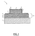
- a typical FBAR-based device is shown in Figure 1.
- the FBAR device 1 comprises a substrate 2, a bottom electrode 4, a piezoelectric layer 6, a top electrode 8 and a passivation layer 10.
- the FBAR device 1 may additionally include an acoustic mirror layer 12, which is comprised of a layer 16 of high acoustic impedance sandwiched between two layers 14 and 18 of low acoustic impedance.
- the mirror usually, but not always, consists of pairs of high and low impedance layers (even number of layers). Some mirror consists of two pairs of such layers arranged in a sequence like SiO2, W, SiO2, W.
- a FBAR device may additionally include one or more membrane layers of SiO2 and a sacrificial layer.
- the substrate 2 can be made from silicon (Si), silicon dioxide (SiO2), Galium Arsenide (GaAs), glass, or ceramic materials.
- the bottom electrode 4 and top electrode 8 can be made from gold (Au), molybdenum (Mo), aluminum (Al), titanium (Ti) or other electrically conductive materials.
- the piezoelectric layer 6 can be made from zinc oxide (ZnO), zinc sulfide (ZnS), aluminum nitride (AlN), lithium tantalate (LiTaO 3 ) or other members of the so-called lead lanthanum zirconate titanate family.
- the passivation layer can be made from SiO2, Si3N4 or polyimide.
- the low acoustic impedance layers 14 and 18 can be made from Si, SiO2, poly-silicon, Al or a polymer.
- the high acoustic impedance layer 16 can be made from Au, Mo or tungsten (W), and in some cases, dielectric such as A1N to make a number of layer pairs.
- FBAR ladder filters are typically designed so that the series resonators yield a series resonance at a frequency that is approximately equal to, or near, the desired, or designed, center frequency of the respective filters.
- the shunt, or parallel, resonators yield a parallel resonance at a frequency slightly offset from the series FBAR resonance.
- the series resonators are usually designed to have their maximum peak in transmission at the center frequency, so that signals are transmitted through the series resonators.
- the parallel resonators are designed to have their minimum in transmission so that signals are not shorted to ground.
- FBARs yield parallel resonance and series resonance at frequencies that differ by an amount that is a function of a piezoelectric coefficient of the piezoelectric materials used to fabricate the devices, in addition to other factors such as the types of layers and other materials employed within in the device.
- FBAR ladder filters yield passbands having bandwidths that are a function of, for example, the types of materials used to form the piezoelectric layers of the resonators and the thickness of various layers in the device.
- FBARs are fabricated on a glass substrate or a silicon wafer.
- the various layers in the FBAR-based device are sequentially formed by thin-film deposition.
- the resonant frequency of the device usually has to be controlled to within a 0.2-0.5% tolerance. This means that the thickness of each layer in the device must be controlled in the same way. It is known that, however, the deposition of thin-film layers is difficult to control to yield a thickness within such tolerance when the area of substrate or wafer is large. For that reason, manufacturers of FBAR-based devices use wafers of 4-inches or less in diameter for device fabrication.
- This object can be achieved by correcting for the thickness non-uniformity of the devices fabricated on large substrates.
- the thickness variations can be corrected by selectively removing material from or adding material to the surface area of a wafer (with one or more layers of the device already deposited thereon), or die, before the wafer is cut into individual chips.
- the bulk acoustic wave device refers to the entire wafer or substrate that has one or more layers deposited thereon to form one or more individual chips, or part of such wafer or substrate.
- the bulk acoustic wave devices referred to herein include bulk acoustic wave resonators, stacked crystal filters, any combination of the resonators and filters, and the structural variations of the resonators and filters.
- the device may or may not have all the necessary layers or the patterns of the layers.
- the topmost layer on the substrate may be the piezoelectric layer, the top electrode or another layer.
- a method of tuning a bulk acoustic wave device comprising a substrate and a plurality of acoustic wave generating and controlling layers formed on the substrate, wherein the device has a surface and a thickness, and wherein the device has an operating frequency which varies partly with the thickness of the device and the operating frequency can be adjusted by changing the thickness of the device.
- the method comprises the steps of:
- the aperture be larger than one individual chip or a single resonator or filter so that a sufficiently large portion of the device surface is exposed to the beam at once. It is possible, however, to have a small aperture so that only one or two chips or a portion of a chip on the device is exposed to the beam simultaneously.
- the wafer is mapped to determine the non-uniformity profile of the device surface.
- mapping can be carried out by measuring the frequency of localized areas of the device, or by measuring the thickness of the layer stack. From the mapping result, it is possible to calculate the amount of material to be added to or removed from the device surface as a function of location.
- a top electrode layer is deposited on the piezoelectric layer after the thickness adjustment. It may be necessary to adjust the thickness of the top electrode layer using the same method. Additionally, a patterning step is usually necessary to produce a desired pattern for the electrode layer. The patterning step is not part of the present invention. Furthermore, if a passivation layer is deposited on top of the patterned top-electrode layer, it may be necessary to adjust the thickness of the passivation layer. Thus, the thickness adjustment steps, according to the present invention, may be carried out one or more times for tuning the entire device, if necessary.
- a system for tuning a bulk acoustic wave device comprising a substrate and a plurality of acoustic wave generating and controlling layers formed on the substrate, wherein the device has a surface and a thickness, and wherein the bulk acoustic wave device has an operating frequency, which varies partly with a thickness of the device, and the operating frequency can be adjusted by changing the thickness of the device.
- the system comprises:
- the system also comprises a mechanism of mapping the thickness non-uniformity profile of the device surface prior to adjusting the thickness.
- the mapping mechanism comprises a frequency measurement device for measuring the frequency at different locations of the device surface. It is also possible to use a thickness measurement device to determine the amount of material to be added or removed at different locations.
- Figure 1 is a cross sectional side view of a typical bulk acoustic wave device illustrating a plurality of layers formed on a substrate.
- Figure 2 is a diagrammatic representation illustrating a thickness adjustment system for adding material onto the topmost layer of a bulk acoustic wave device, according to the present invention.
- Figure 3 is a diagrammatic representation illustrating a bulk acoustic wave device after thickness adjustment by adding material from the topmost surface.
- Figure 4 is a diagrammatic representation illustrated a bulk acoustic wave device that has one or more layers fabricated over top of the modified layer.
- Figure 5 is a diagrammatic representation illustrating a thickness adjustment system for removing material from the topmost layer of a bulk acoustic wave device, according to the present invention.
- Figure 6 is a diagrammatic representation illustrating a bulk acoustic wave device after thickness adjustment by removing material from the topmost surface.
- Figure 7a is a diagrammatic representation illustrating a system for mapping a bulk acoustic wave device by measuring the resonant frequency, according the present invention.
- Figure 7b is a diagrammatic representation illustrating a system for mapping a bulk acoustic wave device by measuring the physical thickness of the device, according to the present invention.
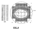
- Figure 8 is a thickness chart illustrating the non-uniformity thickness profile of a wafer with a plurality of acoustic wave generator and control layers fabricated thereon.
- Figure 9 is a flow chart illustrating the steps for tuning a bulk acoustic wave device, according to the present invention.
- the thickness adjustment system 30 comprises a material source 40 to provide added material to a thin-film bulk acoustic device 60 fabricated on a wafer or substrate 62.
- the layers on top of the substrate 62 are collectively referred to as the upper layers and denoted by reference numeral 64.
- the upper layers 64 have a top surface 66.
- the thickness of the upper layers is not uniform.
- the bulk acoustic device 60 may comprise a plurality of individual BAW chips (not shown) each containing one or more resonators and filters. Because of the thickness non-uniformity of the surface 66, some of the individual BAW chips may not meet a specification regarding their resonant frequency. Thus, these individual BAW chips must be tuned.
- the first method involves adding material to the upper surface 66 to fill in the thinner areas of the upper layers 64.
- the other method involves removing part of the upper surface 66, as described in conjunction with Figures 5 and 6 below.
- the material source 40 is used to provide a beam of particles collectively denoted by reference numeral 42.
- a mask 50 having an opening or aperture 52 is placed over the bulk acoustic device 60 so that only a portion 42' of the beam 42 can reach the upper surface 66 in a controlled manner.
- the mask 50 is moved by a moving mechanism 58 in a lateral direction relative to the upper surface 66, as denoted by the arrow 54, so that the entire surface area of the upper layers 64 can be exposed to the particle beam 42 if necessary.
- the thickness of the device 60 is mapped by a mapping mechanism ( Figure 7a and 7b) to determine the non-uniformity profile of the device 60. It is preferred that the non-uniformity profile is determined from measuring the resonant frequency at different surface localities of the device 60, but it is possible to measure the thickness by a thickness measuring means.
- the non-uniformity profile of a wafer (with one or more bulk acoustic generation and control layers fabricated thereon) is shown in Figure 8.
- the thickness profile is denoted by reference numeral 154 and the control program is denoted by reference numeral 152.
- Figure 3 illustrates an adjusted bulk acoustic device 60'.
- a layer of added material 70 on top of the upper layers 64 renders the thickness of the device 60' substantially uniform throughout the device. It is preferred that the added material is the same as the material of the layer directly beneath it.
- the topmost layer of the upper layers 60' is a passivation layer when the device 60 is subject to thickness adjustment, it is preferable to use the same passivation material for the particle beam 42.
- this practice is only preferred, not necessary.
- the thickness profile of the piezoelectric layer may be the most important factor that determines whether the device meets its specification.
- the topmost layer of a bulk acoustic device usually is not a piezoelectric layer. It is, however, possible to adjust the thickness of the piezoelectric layer in a manner, as described in conjunction with Figures 2 and 3, and then add more layers on top of the adjusted piezoelectric layer to complete the device fabrication process.
- one or more layers 68 can be formed over the adjusted upper layer 64.
- the thickness of the new layers 68 is not uniform such that it affects the overall performance of the device, it is possible to adjust the thickness of the new layer 68, using the same process if so desired.
- Figure 5 illustrates a different thickness adjustment system 32.
- an etching apparatus 80 to remove part of the upper surface 66 of the device 60.
- IBE ion beam etching
- RIBE reactive ion beam
- etching techniques such as sputtering and laser ablation
- sputtering and laser ablation can also be used to surface thickness adjustment through the aperture 52 of the mask 50.
- the modified device 60" is shown in Figure 6.
- the upper layer 64' after adjustment, is thinner than the original upper layer 64.
- the upper layer 64 should be made thicker than the specified or targeted thickness.
- a material source 40 is used for surface adjustment, as shown in Figure 2, the upper layer 64 should be made thinner than the specified or targeted thickness.
- the thickness profile Prior to thickness adjustment using a material source 40, as shown in Figure 2, or an etching apparatus 80, as shown in Figure 5, it is preferred that the thickness profile be mapped. It is preferable to use a frequency measurement apparatus 84 to perform localized measurement of the resonant frequency of the device 60. It may be necessary to measure the resonant frequency of the individual resonators and filters of the device 60. It should be noted that, in order to measure the resonant frequency of those components, it is necessary to form and pattern the top electrode layer on the wafer. Base on the frequency profile 150, it is possible to calculate the amount of material to be removed from or added on the upper surface 66.
- the profile mapping system 34 comprises a frequency measurement apparatus 84, and a moving mechanism 88 for moving the frequency measurement apparatus 84 relative to the device 60 for obtaining the frequency profile 150 of the surface. From the frequency profile 150 it is possible to obtain the thickness non-uniformity profile 154 ( Figures 2 and 5).
- Figure 7b is a diagrammatic representation illustrating a system 36 for mapping a bulk acoustic wave device by measuring the physical thickness of the device. Instead of a frequency measurement apparatus 84, a thickness measurement apparatus 86 is used to measure the thickness of the device 60 directly.
- Figure 8 is a thickness chart illustrating the non-uniformity thickness profile of a wafer with a plurality of acoustic wave generating and controlling layers fabricated thereon.
- Figure 8 shows the non-uniformity profile of a piezoelectric (ZnO) layer expressed in terms of nanometers. If the average thickness is used as a reference, then the thickness variation across the layer is about ⁇ 23%. With such a large variation in thickness, the frequency variation across the wafer is usually not acceptable. Thus, the device must be tuned by adjusting the thickness of the device.
- Figure 9 is a flow chart illustrating the process 100 for tuning a bulk acoustic wave device, according to the present invention.
- a frequency measurement apparatus Figure 7a
- a thickness measurement apparatus Figure 7b
- a thickness non-uniformity profile 154 is thus obtained. If the surface thickness falls within the tolerance, as determined at step 103, then new layers may be added on top of the mapped surface. Otherwise, a mask 50 with an aperture 52 is placed over the device 60 ( Figures 2 and 5) at step 104. A beam of particles is applied over the mask 50 to allow part of beam to go through the aperture 52 to make contact with the device surface at a local area, at step 106.
- the thickness of the local area is adjusted using the particle beam, it is determined, at step 108, whether the necessary thickness adjustment of the entire surface is carried out. If the thickness of more surface area needs to be adjusted, the mask 50 is moved to another unadjusted location, at step 110. If the necessary thickness of the entire surface has been carried out, it is determined, at step 112, whether more layers need to be fabricated to complete the device. After one or more new layers are added, at step 114, on top of the adjusted layer, the surface profile of the device is again mapped, at step 102, to determine whether the device is made according to the specification.
- the present invention discloses a method and system for tuning the bulk acoustic wave device at a wafer, or die, level.
- the method and system, as disclosed, are particularly useful when the surface area of the wafer is sufficiently large such that the deposition of thin-film cannot achieve acceptable thickness uniformity. Trimming the frequency across the wafer by adjusting the thickness at localized areas of the wafer surface can increase the yield of the FBAR manufactory process.
- the thickness adjustment process can be separately and sequentially carried out to adjust at one or more layers of the FBAR-based device. If a material is added onto a surface layer to trim the frequency and a material source is used to provide a beam of particles, it is preferable that the particles and the surface layer are of the same material.
- the material for the particles and the material for the surface layer may not be the same. If the material of the surface layer is partially removed to trim the frequency, it is preferred to use a dry etching process, such as IBE or RIBE, to trim the surface. However, other surface removal process, such as sputtering, can be used to achieve the same objective. It is known in the art that the fabrication of the top and bottom electrode layers, in general, involves one or more additional steps to make a pattern out of each of the electrode layers. It is preferred that the patterning steps are carried out after the thickness of the respective electrode layer is adjusted. However, it is also possible to carry out the patterning steps prior to the thickness adjustment.
- the mask as described hereinabove, has one aperture to allow the particle to make contact with the device surface. It is possible to have two or more apertures on the mask for surface thickness adjustment. Moreover, it is possible to move the mask relative to the device to relocate the aperture on the mask. It is also possible to move the device relative to mask to achieve the same.
Landscapes
- Engineering & Computer Science (AREA)
- Manufacturing & Machinery (AREA)
- Piezo-Electric Or Mechanical Vibrators, Or Delay Or Filter Circuits (AREA)
- Surface Acoustic Wave Elements And Circuit Networks Thereof (AREA)
- Length Measuring Devices Characterised By Use Of Acoustic Means (AREA)
Applications Claiming Priority (2)
| Application Number | Priority Date | Filing Date | Title |
|---|---|---|---|
| US09/784,634 US6456173B1 (en) | 2001-02-15 | 2001-02-15 | Method and system for wafer-level tuning of bulk acoustic wave resonators and filters |
| US784634 | 2001-02-15 |
Publications (3)
| Publication Number | Publication Date |
|---|---|
| EP1233510A2 true EP1233510A2 (fr) | 2002-08-21 |
| EP1233510A3 EP1233510A3 (fr) | 2003-04-02 |
| EP1233510B1 EP1233510B1 (fr) | 2008-10-29 |
Family
ID=25133066
Family Applications (1)
| Application Number | Title | Priority Date | Filing Date |
|---|---|---|---|
| EP02250518A Expired - Lifetime EP1233510B1 (fr) | 2001-02-15 | 2002-01-25 | Procédé d'accordage d'un dispositif à ondes acoustiques de volume |
Country Status (4)
| Country | Link |
|---|---|
| US (1) | US6456173B1 (fr) |
| EP (1) | EP1233510B1 (fr) |
| JP (1) | JP4130990B2 (fr) |
| DE (1) | DE60229577D1 (fr) |
Cited By (5)
| Publication number | Priority date | Publication date | Assignee | Title |
|---|---|---|---|---|
| EP1258988A3 (fr) * | 2001-04-27 | 2004-02-04 | Nokia Corporation | Procédé et système d'accordage de résonateurs et filtres à ondes acoustiques de volume au niveau de la plaquette |
| EP1816233A3 (fr) * | 2001-05-22 | 2007-08-22 | Infineon Technologies AG | Procédé de fabrication d'une couche dotée d'un profil d'épaisseur de couche prédéfini |
| EP1258987B1 (fr) * | 2001-04-27 | 2007-11-21 | Nokia Corporation | Procédé et système d'accordage de résonateurs et filtres à ondes acoustiques de volume au niveau de la plaquette |
| EP2017958A3 (fr) * | 2007-06-15 | 2009-02-25 | Infineon Technologies AG | Structure de résonateur piézoélectrique et procédé de fabrication d'un dispositif de résonateur couplé |
| WO2012049373A1 (fr) * | 2010-10-14 | 2012-04-19 | Teknologian Tutkimuskeskus Vtt | Changement de fréquence de fonctionnement dans un filtre à ondes acoustiques de volume à couplage latéral |
Families Citing this family (22)
| Publication number | Priority date | Publication date | Assignee | Title |
|---|---|---|---|---|
| JP3470678B2 (ja) * | 2000-03-31 | 2003-11-25 | 株式会社村田製作所 | 電子部品の周波数調整方法 |
| KR100398363B1 (ko) * | 2000-12-05 | 2003-09-19 | 삼성전기주식회사 | Fbar 소자 및 그 제조방법 |
| WO2002076666A2 (fr) * | 2001-03-22 | 2002-10-03 | Xsil Technology Limited | Systeme et procede d'usinage par laser |
| TW591202B (en) * | 2001-10-26 | 2004-06-11 | Hermosa Thin Film Co Ltd | Dynamic film thickness control device/method and ITS coating method |
| US6662419B2 (en) * | 2001-12-17 | 2003-12-16 | Intel Corporation | Method for fabricating film bulk acoustic resonators to achieve high-Q and low loss |
| US6949268B2 (en) * | 2002-06-28 | 2005-09-27 | Intel Corporation | Frequency uniformity of film bulk acoustic resonators |
| US6787970B2 (en) * | 2003-01-29 | 2004-09-07 | Intel Corporation | Tuning of packaged film bulk acoustic resonator filters |
| GB0308249D0 (en) * | 2003-04-10 | 2003-05-14 | Trikon Technologies Ltd | Method of depositing piezoelectric films |
| US20040227578A1 (en) * | 2003-05-14 | 2004-11-18 | Miikka Hamalainen | Acoustic resonance-based frequency synthesizer using at least one bulk acoustic wave (BAW) or thin film bulk acoustic wave (FBAR) device |
| US7114252B2 (en) * | 2004-06-17 | 2006-10-03 | Toko, Inc. | Large scale simultaneous circuit encapsulating apparatus |
| US20060017352A1 (en) * | 2004-07-20 | 2006-01-26 | Aram Tanielian | Thin device and method of fabrication |
| US20070139140A1 (en) * | 2005-12-20 | 2007-06-21 | Rao Valluri R | Frequency tuning of film bulk acoustic resonators (FBAR) |
| JP5036215B2 (ja) * | 2006-05-19 | 2012-09-26 | 日本碍子株式会社 | 圧電薄膜共振子及び圧電薄膜共振子の共振周波数の調整方法 |
| DE102008003820B4 (de) * | 2008-01-10 | 2013-01-17 | Epcos Ag | Frontendschaltung |
| US20110121916A1 (en) * | 2009-11-24 | 2011-05-26 | Avago Technologies Wireless Ip (Singapore) Pte. Ltd. | Hybrid bulk acoustic wave resonator |
| JP5617523B2 (ja) * | 2009-12-08 | 2014-11-05 | 株式会社村田製作所 | 積層型圧電薄膜フィルタの製造方法 |
| US8922302B2 (en) | 2011-08-24 | 2014-12-30 | Avago Technologies General Ip (Singapore) Pte. Ltd. | Acoustic resonator formed on a pedestal |
| US9166141B2 (en) * | 2011-09-09 | 2015-10-20 | Dvx, Llc | Process of manufacturing a piezopolymer transducer with matching layer |
| CN109474254B (zh) | 2018-10-31 | 2020-12-08 | 武汉衍熙微器件有限公司 | 一种声波器件及其制作方法 |
| CN111058005A (zh) * | 2019-08-09 | 2020-04-24 | 河源市众拓光电科技有限公司 | 一种氮化物和金属薄膜沉积与修整设备及其应用 |
| CN114244300A (zh) * | 2020-09-09 | 2022-03-25 | 诺思(天津)微系统有限责任公司 | 滤波器组件及其制造方法、电子设备 |
| CN119382650B (zh) * | 2024-12-31 | 2025-04-11 | 天通瑞宏科技有限公司 | 一种滤波器的频率修调方法、装置、设备及介质 |
Family Cites Families (15)
| Publication number | Priority date | Publication date | Assignee | Title |
|---|---|---|---|---|
| US4454639A (en) * | 1982-06-03 | 1984-06-19 | Motorola, Inc. | Method for tuning piezoelectric resonators |
| US4638536A (en) * | 1986-01-17 | 1987-01-27 | The United States Of America As Represented By The Secretary Of The Army | Method of making a resonator having a desired frequency from a quartz crystal resonator plate |
| US4761298A (en) * | 1987-05-06 | 1988-08-02 | The United States Of America As Represented By The Secretary Of The Army | Method of precisely adjusting the frequency of a piezoelectric resonator |
| US5643629A (en) * | 1991-05-20 | 1997-07-01 | Sauerland; Franz L. | Method for adjusting center frequency and bandwidth of monolithic filters by plating through a single-aperture mask on a single side of the filters electrode pattern to plate selected areas of the pattern |
| FR2699765B1 (fr) * | 1992-12-22 | 1995-01-20 | Cepe | Procédé d'ajustage en fréquence d'un dispositif piézoélectrique et équipement pour la mise en Óoeuvre du procédé. |
| US5587620A (en) * | 1993-12-21 | 1996-12-24 | Hewlett-Packard Company | Tunable thin film acoustic resonators and method for making the same |
| US5662782A (en) * | 1994-05-26 | 1997-09-02 | Seiko Epson Corporation | Method and apparatus for adjusting a resonance frequency of piezoelectric elements |
| JPH0818372A (ja) * | 1994-06-24 | 1996-01-19 | Seiko Instr Inc | 圧電素子の周波数調整装置及び圧電周波数調整方法 |
| US5630949A (en) * | 1995-06-01 | 1997-05-20 | Tfr Technologies, Inc. | Method and apparatus for fabricating a piezoelectric resonator to a resonant frequency |
| US6051907A (en) * | 1996-10-10 | 2000-04-18 | Nokia Mobile Phones Limited | Method for performing on-wafer tuning of thin film bulk acoustic wave resonators (FBARS) |
| US5780713A (en) * | 1996-11-19 | 1998-07-14 | Hewlett-Packard Company | Post-fabrication tuning of acoustic resonators |
| US5894647A (en) * | 1997-06-30 | 1999-04-20 | Tfr Technologies, Inc. | Method for fabricating piezoelectric resonators and product |
| US6081171A (en) | 1998-04-08 | 2000-06-27 | Nokia Mobile Phones Limited | Monolithic filters utilizing thin film bulk acoustic wave devices and minimum passive components for controlling the shape and width of a passband response |
| US6339276B1 (en) * | 1999-11-01 | 2002-01-15 | Agere Systems Guardian Corp. | Incremental tuning process for electrical resonators based on mechanical motion |
| US6307447B1 (en) * | 1999-11-01 | 2001-10-23 | Agere Systems Guardian Corp. | Tuning mechanical resonators for electrical filter |
-
2001
- 2001-02-15 US US09/784,634 patent/US6456173B1/en not_active Expired - Fee Related
-
2002
- 2002-01-25 EP EP02250518A patent/EP1233510B1/fr not_active Expired - Lifetime
- 2002-01-25 DE DE60229577T patent/DE60229577D1/de not_active Expired - Lifetime
- 2002-01-28 JP JP2002018553A patent/JP4130990B2/ja not_active Expired - Fee Related
Cited By (6)
| Publication number | Priority date | Publication date | Assignee | Title |
|---|---|---|---|---|
| EP1258988A3 (fr) * | 2001-04-27 | 2004-02-04 | Nokia Corporation | Procédé et système d'accordage de résonateurs et filtres à ondes acoustiques de volume au niveau de la plaquette |
| EP1258987B1 (fr) * | 2001-04-27 | 2007-11-21 | Nokia Corporation | Procédé et système d'accordage de résonateurs et filtres à ondes acoustiques de volume au niveau de la plaquette |
| EP1816233A3 (fr) * | 2001-05-22 | 2007-08-22 | Infineon Technologies AG | Procédé de fabrication d'une couche dotée d'un profil d'épaisseur de couche prédéfini |
| EP2017958A3 (fr) * | 2007-06-15 | 2009-02-25 | Infineon Technologies AG | Structure de résonateur piézoélectrique et procédé de fabrication d'un dispositif de résonateur couplé |
| US7535324B2 (en) | 2007-06-15 | 2009-05-19 | Avago Technologies Wireless Ip, Pte. Ltd. | Piezoelectric resonator structure and method for manufacturing a coupled resonator device |
| WO2012049373A1 (fr) * | 2010-10-14 | 2012-04-19 | Teknologian Tutkimuskeskus Vtt | Changement de fréquence de fonctionnement dans un filtre à ondes acoustiques de volume à couplage latéral |
Also Published As
| Publication number | Publication date |
|---|---|
| EP1233510A3 (fr) | 2003-04-02 |
| US6456173B1 (en) | 2002-09-24 |
| JP2002311959A (ja) | 2002-10-25 |
| EP1233510B1 (fr) | 2008-10-29 |
| JP4130990B2 (ja) | 2008-08-13 |
| DE60229577D1 (de) | 2008-12-11 |
| US20020109565A1 (en) | 2002-08-15 |
Similar Documents
| Publication | Publication Date | Title |
|---|---|---|
| US6456173B1 (en) | Method and system for wafer-level tuning of bulk acoustic wave resonators and filters | |
| US6441702B1 (en) | Method and system for wafer-level tuning of bulk acoustic wave resonators and filters | |
| EP1258988B1 (fr) | Procédé et système d'accordage de résonateurs et filtres à ondes acoustiques de volume au niveau de la plaquette | |
| EP1258987B1 (fr) | Procédé et système d'accordage de résonateurs et filtres à ondes acoustiques de volume au niveau de la plaquette | |
| JP4648911B2 (ja) | 振幅変調および位相変調を行うための整調可能な薄膜バルク型音響共振器が組み込まれている装置 | |
| US7109826B2 (en) | Tapered electrode in an acoustic resonator | |
| US6476536B1 (en) | Method of tuning BAW resonators | |
| US6774746B2 (en) | Thin film bulk acoustic resonator filters with a piezoelectric layer of lead scandium tantalum oxide | |
| US8610333B2 (en) | Acoustic wave devices | |
| US20060017352A1 (en) | Thin device and method of fabrication | |
| US20040017130A1 (en) | Adjusting the frequency of film bulk acoustic resonators | |
| US8479363B2 (en) | Methods for wafer level trimming of acoustically coupled resonator filter | |
| EP1489740A2 (fr) | Composant électronique et procédé de fabrication de celui-ci | |
| US8091190B2 (en) | Method of manufacturing an acoustic mirror for a piezoelectric resonator | |
| CN115250099A (zh) | 调整谐振频率的方法、谐振器、滤波器及半导体器件 | |
| US6975184B2 (en) | Adjusting the frequency of film bulk acoustic resonators | |
| US6867667B2 (en) | Piezoelectric filter, communication device, and method for manufacturing communication device | |
| CN114928348A (zh) | 一种滤波器、通信设备及其制造方法 | |
| US20220376673A1 (en) | Baw resonator arrangement with resonators having different resonance frequencies and manufacturing method | |
| CN115296634A (zh) | 一种空气隙薄膜体声波滤波器及其制备方法 |
Legal Events
| Date | Code | Title | Description |
|---|---|---|---|
| PUAI | Public reference made under article 153(3) epc to a published international application that has entered the european phase |
Free format text: ORIGINAL CODE: 0009012 |
|
| AK | Designated contracting states |
Kind code of ref document: A2 Designated state(s): AT BE CH CY DE DK ES FI FR GB GR IE IT LI LU MC NL PT SE TR |
|
| AX | Request for extension of the european patent |
Free format text: AL;LT;LV;MK;RO;SI |
|
| PUAL | Search report despatched |
Free format text: ORIGINAL CODE: 0009013 |
|
| AK | Designated contracting states |
Kind code of ref document: A3 Designated state(s): AT BE CH CY DE DK ES FI FR GB GR IE IT LI LU MC NL PT SE TR |
|
| AX | Request for extension of the european patent |
Extension state: AL LT LV MK RO SI |
|
| 17P | Request for examination filed |
Effective date: 20030515 |
|
| AKX | Designation fees paid |
Designated state(s): DE FR GB IT |
|
| 17Q | First examination report despatched |
Effective date: 20061221 |
|
| GRAP | Despatch of communication of intention to grant a patent |
Free format text: ORIGINAL CODE: EPIDOSNIGR1 |
|
| GRAC | Information related to communication of intention to grant a patent modified |
Free format text: ORIGINAL CODE: EPIDOSCIGR1 |
|
| RAP1 | Party data changed (applicant data changed or rights of an application transferred) |
Owner name: AVAGO TECHNOLOGIES WIRELESS IP (SINGAPORE) PTE. LT |
|
| GRAS | Grant fee paid |
Free format text: ORIGINAL CODE: EPIDOSNIGR3 |
|
| GRAA | (expected) grant |
Free format text: ORIGINAL CODE: 0009210 |
|
| AK | Designated contracting states |
Kind code of ref document: B1 Designated state(s): DE FR GB IT |
|
| REG | Reference to a national code |
Ref country code: GB Ref legal event code: FG4D |
|
| REF | Corresponds to: |
Ref document number: 60229577 Country of ref document: DE Date of ref document: 20081211 Kind code of ref document: P |
|
| PG25 | Lapsed in a contracting state [announced via postgrant information from national office to epo] |
Ref country code: IT Free format text: LAPSE BECAUSE OF FAILURE TO SUBMIT A TRANSLATION OF THE DESCRIPTION OR TO PAY THE FEE WITHIN THE PRESCRIBED TIME-LIMIT Effective date: 20081029 |
|
| PLBE | No opposition filed within time limit |
Free format text: ORIGINAL CODE: 0009261 |
|
| STAA | Information on the status of an ep patent application or granted ep patent |
Free format text: STATUS: NO OPPOSITION FILED WITHIN TIME LIMIT |
|
| GBPC | Gb: european patent ceased through non-payment of renewal fee |
Effective date: 20090129 |
|
| 26N | No opposition filed |
Effective date: 20090730 |
|
| REG | Reference to a national code |
Ref country code: FR Ref legal event code: ST Effective date: 20091030 |
|
| PG25 | Lapsed in a contracting state [announced via postgrant information from national office to epo] |
Ref country code: GB Free format text: LAPSE BECAUSE OF NON-PAYMENT OF DUE FEES Effective date: 20090129 |
|
| PG25 | Lapsed in a contracting state [announced via postgrant information from national office to epo] |
Ref country code: FR Free format text: LAPSE BECAUSE OF NON-PAYMENT OF DUE FEES Effective date: 20090202 |
|
| PGFP | Annual fee paid to national office [announced via postgrant information from national office to epo] |
Ref country code: DE Payment date: 20130123 Year of fee payment: 12 |
|
| REG | Reference to a national code |
Ref country code: DE Ref legal event code: R081 Ref document number: 60229577 Country of ref document: DE Owner name: AVAGO TECHNOLOGIES GENERAL IP (SINGAPORE) PTE., SG Free format text: FORMER OWNER: AVAGO TECHNOLOGIES WIRELESS IP (SINGAPORE) PTE. LTD., SINGAPORE, SG Effective date: 20130606 Ref country code: DE Ref legal event code: R082 Ref document number: 60229577 Country of ref document: DE Representative=s name: DILG HAEUSLER SCHINDELMANN PATENTANWALTSGESELL, DE Effective date: 20130606 |
|
| REG | Reference to a national code |
Ref country code: DE Ref legal event code: R119 Ref document number: 60229577 Country of ref document: DE |
|
| REG | Reference to a national code |
Ref country code: DE Ref legal event code: R119 Ref document number: 60229577 Country of ref document: DE Effective date: 20140801 |
|
| PG25 | Lapsed in a contracting state [announced via postgrant information from national office to epo] |
Ref country code: DE Free format text: LAPSE BECAUSE OF NON-PAYMENT OF DUE FEES Effective date: 20140801 |