EP1235252A2 - Ionenstrahlabtastverfahren und vorrichtung in einem Ionenimplantationsgerät - Google Patents
Ionenstrahlabtastverfahren und vorrichtung in einem Ionenimplantationsgerät Download PDFInfo
- Publication number
- EP1235252A2 EP1235252A2 EP02076746A EP02076746A EP1235252A2 EP 1235252 A2 EP1235252 A2 EP 1235252A2 EP 02076746 A EP02076746 A EP 02076746A EP 02076746 A EP02076746 A EP 02076746A EP 1235252 A2 EP1235252 A2 EP 1235252A2
- Authority
- EP
- European Patent Office
- Prior art keywords
- ion
- ions
- mass
- extraction assembly
- ion source
- Prior art date
- Legal status (The legal status is an assumption and is not a legal conclusion. Google has not performed a legal analysis and makes no representation as to the accuracy of the status listed.)
- Withdrawn
Links
Images

Classifications
-
- H—ELECTRICITY
- H01—ELECTRIC ELEMENTS
- H01J—ELECTRIC DISCHARGE TUBES OR DISCHARGE LAMPS
- H01J37/00—Discharge tubes with provision for introducing objects or material to be exposed to the discharge, e.g. for the purpose of examination or processing thereof
- H01J37/02—Details
- H01J37/04—Arrangements of electrodes and associated parts for generating or controlling the discharge, e.g. electron-optical arrangement or ion-optical arrangement
- H01J37/147—Arrangements for directing or deflecting the discharge along a desired path
- H01J37/1472—Deflecting along given lines
- H01J37/1474—Scanning means
- H01J37/1477—Scanning means electrostatic
-
- H—ELECTRICITY
- H01—ELECTRIC ELEMENTS
- H01J—ELECTRIC DISCHARGE TUBES OR DISCHARGE LAMPS
- H01J37/00—Discharge tubes with provision for introducing objects or material to be exposed to the discharge, e.g. for the purpose of examination or processing thereof
- H01J37/02—Details
- H01J37/04—Arrangements of electrodes and associated parts for generating or controlling the discharge, e.g. electron-optical arrangement or ion-optical arrangement
- H01J37/08—Ion sources; Ion guns
-
- H—ELECTRICITY
- H01—ELECTRIC ELEMENTS
- H01J—ELECTRIC DISCHARGE TUBES OR DISCHARGE LAMPS
- H01J37/00—Discharge tubes with provision for introducing objects or material to be exposed to the discharge, e.g. for the purpose of examination or processing thereof
- H01J37/30—Electron-beam or ion-beam tubes for localised treatment of objects
- H01J37/317—Electron-beam or ion-beam tubes for localised treatment of objects for changing properties of the objects or for applying thin layers thereon, e.g. for ion implantation
- H01J37/3171—Electron-beam or ion-beam tubes for localised treatment of objects for changing properties of the objects or for applying thin layers thereon, e.g. for ion implantation for ion implantation
Definitions
- the invention relates to ion beam scanning in, but not limited to, ion implanter systems for implanting ions from an ion beam into target substrates such as semiconductor wafers. More specifically the invention relates to apparatus and method for scanning the ion beam at the point of extraction of the ion beam from an ion source.
- Ion implantation techniques e.g. for modifying the electrical conductivity properties of semiconductor materials, are known in the manufacture of integrated circuit structures in semiconductor wafers.
- Such ion implanters generally comprise an ion beam generator having a source of ions of the element to be implanted in the semiconductor wafer, and an extraction assembly for extracting ions from the source and forming a beam of the extracted ions.
- the ion beam so produced is then passed through a mass analyser and selector for selecting a particular species of ions in the ion beam for onward transmission for implantation in the wafer or target substrate.
- the substrate and the ion beam are scanned relative to each other so that in one process treatment the dose at any position on the target substrate is made up of components from a large number of individual scans.
- a common scanning technique used in the prior art involves mechanically moving the target substrate relative to a stationary beam. The target substrate is mechanically scanned in two dimensions. Apparatus of this kind is described for example in US5389793.
- a number of target substrates are mounted on a rotatable wheel, whereby rotation of the wheel in the process chamber of the implant tool provides the scan of each of the target substrates mounted on the wheel in one direction, and reciprocating movement of the axis of rotation provides the scanning movement in a second direction.
- the physical speed of relative scanning of target substrate and ion beam by mechanical means limits the minimum process time possible with such mechanical scanning implanters, if a certain minimum number of repeat scans is required for each substrate in order to ensure adequate homogeneity of dose over the substrate surface.
- a batch of target substrates are processed simultaneously in order to provide adequate throughput for the implant machines.
- the wafers are mounted on the wheel on mounting surfaces which are angled relative to the plane of rotation slightly inwards towards the axis of rotation. In this way, the wafers are held firmly against the wafer support surfaces by centrifugal force.
- the wafers are therefore distributed on the process wheel on a shallow conical surface and are scanned in this conical surface through the beam during processing. As a result, the angle between the beam and the wafer changes slightly as the wafer is scanned through the beam, resulting in a small non-uniformity of the angle of implantation of ions into the wafer.
- single wafer implanters have been proposed in which the fast scanning of the ion beam relative to the wafer in one co-ordinate direction is performed by electrostatic or electromagnetic scanning of the beam, while the slower rate scanning in the orthogonal co-ordinate direction is performed by mechanically moving the wafer.
- ion beams may be theoretically scanned either electrostatically or electromagnetically, there are well established problems with electrostatic scanning. It is well known to those experienced in this field that difficulties arise in controlling ion beams, especially at relatively lower energies, when the ion beam travels through regions of electric field. These problems arise because electrons cannot exist for substantial times in regions of electric field, so that beams of positive ions can experience severe space charge effects in the absence of neutralising electrons in such regions. As a result, the ion beam tends to "blow up" and become uncontrollable.
- the above described magnetic beam scanning proposal still occupies substantial space and the scanning magnet may be expensive and require expensive HF power amplifiers. Further, it is believed that electromagnetic scanning of the ion beam may also compromise the space charge neutralisation of the ion beam, especially in the scanning region. This may become especially a problem for relatively low energy ion beams.
- EP-A-0145119 discloses an ion implanter with an ion source extraction assembly having a first electrode forming a front face of the ion source arc chamber, a second fringe electrode having components on opposite sides of the extracted beam, a third extraction electrode and a fourth ground electrode.
- the present invention relates to an ion implanter for implanting ions in a target substrate in which the ion beam is scanned at an extraction point of the ion beam. More specifically, the present invention is an ion implanter for implanting ions in a target substrate and comprising an ion source, an ion beam extraction assembly for extracting ions from the ion source and forming a beam of the extracted ions, a target substrate holder, and an ion mass selector located between the extraction assembly and the substrate holder.
- the ion mass selector is effective to select ions of a desired mass in said beam of extracted ions for implanting in the target substrate.
- the extraction assembly is arranged for controllably deflecting the beam of extracted ions over a predetermined maximum deflection angle at least in a deflection plane.
- the ion mass selector is then operative to select ions of the desired mass in the deflected beam over this maximum deflection angle.
- a beam of mass selected ions can then be scanned over the target substrate by controlling the deflection angle at the extraction assembly.
- the relatively bulky magnetic scanning magnet can be dispensed with, thereby reducing the size of the implanter.
- beam deflection is performed electrostatically at the extraction point of the beam from the ion source, where an extraction electric field exists already. As a result, beam deflection is achieved without providing an additional region along the beam path at which space charge neutralisation of the beam can be compromised.
- said ion source comprises an arc chamber in which ions are formed, said arc chamber having a front face with an exit aperture through which ions can be extracted from the arc chamber
- said extraction assembly comprises an electrostatic deflection lens having electrodes located externally of said exit aperture to be on opposite sides of an ion beam emerging from said exit aperture, a first voltage supply connected to apply an extraction potential difference between the arc chamber front face and the electrodes of the deflection lens in common, and a second voltage supply connected to apply a deflection potential difference between electrodes of said lens.
- the extraction assembly may further comprise a shield electrode at the potential of the ion mass selector located between the ion mass selector and said deflection lens, a suppression electrode between said shield electrode and said deflection lens, a third voltage supply connected to bias the arc chamber relative to said shield electrode at a potential corresponding to the desired energy of the ion beam supplied to the ion mass selector, and a fourth voltage supply connected to maintain said suppression electrode at a negative potential relative to said shield electrode.
- the specification also discloses an electrode assembly for extracting ions from an arc chamber and forming a steerable beam of the extracted ions, the electrode assembly comprising a first apertured electrode adapted to form a front face of the arc chamber and forming an exit aperture through which ions can be extracted from the arc chamber, a second apertured electrode adjacent the first electrode and having electrically separate components forming opposite sides of the aperture of said second electrode to form an electrostatic deflection lens, a third apertured electrode adjacent said second electrode and a fourth apertured electrode adjacent said third electrode, said first, second, third and fourth electrodes being electrically insulated from one another.
- the specification further discloses a method of scanning an ion beam across a target substrate in an ion implanter comprising an ion source, an ion beam extraction assembly for extracting ions from the ion source and forming a beam of the extracted ions at a predetermined energy, a holder for the target substrate, and an ion mass selector between said extraction assembly and said substrate holder for selecting ions of a desired mass in said beam of extracted ions for implanting in said target substrate, the method comprising electrostatically deflecting the ions in the extraction assembly transversely of the beam direction at a position where the ions experience an accelerating or decelerating field in the beam direction, thereby angularly steering the direction of said beam, passing the steered beam through the ion mass selector to provide a steered beam of mass selected ions, and changing the angle of said beam of extracted ions to scan the beam of mass selected ions across the target substrate.
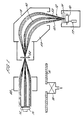
- an ion implanter apparatus embodying the present invention comprises an ion beam source 10 with an extraction assembly 11, directing an ion beam 12 through an ion mass selector 13 to impinge on a target substrate 14 mounted on a target substrate holder 15.
- the above elements of the ion implanter are housed in a vacuum housing of which a part 15 only is illustrated in the Figure.
- the vacuum housing may be evacuated by a vacuum pump 16.
- the ion source 10 may comprise any known ion source such as a Freeman source or a Bernas source.
- the ion source 10 comprises an arc chamber to which is fed a supply of atoms of or molecules containing the element, ions of which are to be implanted in the target substrate 14.
- the molecules may be supplied to the arc chamber in gaseous or vapour form, e.g. from a gas bottle 17.
- the extraction assembly 11 comprises a number of electrodes located immediately outside a front face of the arc chamber of the ion source 10 so as to extract ions from the arc chamber through an exit aperture in the front face.
- the arc chamber of the ion source is represented by the box 20 and ions formed in the arc chamber are extracted from the source 20 through an exit aperture 21 in a front face 22 of the source.
- the front face 22 of the ion source 20 forms a first apertured electrode at the potential of the ion source.
- the extraction assembly 11 ( Figure 1) is illustrated in Figure 2 by second, third and fourth apertured electrodes 23, 24 and 25 repsectively.
- Each of apertured electrodes 24 and 25 comprise a single electrically conductive plate having an aperture through the plate to allow the ion beam emerging from the ion source 20 to pass through.
- Electrode 23, however, comprises electrically separate, i.e.
- the ion source 20 is maintained by a voltage supply 28 at a positive voltage relative to ground 29.
- the fourth apertured electrode 25 is a ground electrode which restricts the penetration of the electric fields between the ground electrode 25 and the ion source 20 into the region to the right (in Figure 2) of the electrode 25.
- the energy of the ion beam emerging from the extraction assembly is determined by the voltage of the voltage supply unit 28. A typical value for this voltage is 20 kV, providing an extracted beam energy of 20 keV. However extracted beam energies of 80 keV and higher, or 2 keV or lower may also be contemplated.
- the third electrode 24 operates as a suppression electrode and is biased by a voltage supply 30 to a negative potential relative to ground 29.
- the negatively biased suppression electrode 24, operates to prevent electrons in the ion beam downstream of the ground electrode 25 (to the right in Figure 2) from being drawn into the extraction region and into the ion source. As is known to workers in this field, it is important to minimise the loss of electrons from the ion beam in zero electric field regions, so as to maintain ion beam neutralisation.
- the second electrode 23 forms a deflection lens and the electrically separate upper and lower parts 26 and 27 can be held at different voltages to produce a transverse electric field component across the ion beam which can deflect the ion beam emerging from the ion source 20.
- the differential voltage supply to the separate components 26 and 27 of the electrode 23 may be derived from a sawtooth voltage generator 31 feeding a differential unit 32 providing phase and antiphase components of the sawtooth waveform on respective outputs 33 and 34. These antiphase components are applied via amplifiers 35 and 36 to respective ones of the components 26 and 27 of the electrode 23.
- the precise shape of the waveform is selected to provide a desired uniform implant dose over the wafer.
- the entire sawtooth voltage supply assembly 37 is held at a negative potential relative to the ion source 21 by a voltage supply unit 38.
- the output voltage of the supply 38 may typically be 15 kV, although higher and lower voltages are also possible.
- the value of the power supply 38 is set to optimise the extraction efficiency of ions from the ion source 20.
- the differential voltage applied between the components 26 and 27 of the electrode 23 may typically have an amplitude considerably less than the value of the output voltage of the power supply 38. Typical differential sawtooth amplitudes on each of the electrode components 26 and 27 are plus or minus 500 volts.
- the power supply for the sawtooth differential supply 37 is supplied along lines 40 via a first isolator 41 to a power bus 42 on a chassis at the potential of the ion source 20, and then via a second isolator to the sawtooth voltage supply 37 which is at the potential relative to the ion source set by the power supply 38.
- the extraction assembly illustrated in Figure 2, comprising first, second, third and fourth electrodes as mentioned above, is a tetrode structure which has the following advantages.
- the potential between the arc chamber of the ion source 20 and the second electrode 23, immediately exterior to the exit aperture of the ion source, can be set independently of the potential between the ion source and ground (the shield electrode 25). In this way, the energy of the ion beam emerging from the extraction assembly can be determined independently of the potential at which ions are initially extracted from the arc chamber.
- Prior art triode extraction assemblies, which dispense with the second electrode 23, require mechanical adjustment of the electrodes to be made in order to optimise or "tune" the ion source for maximum beam current on the target substrate.
- the second electrode is in two parts allowing a transverse electric field component to be generated between them.
- the beam drawn from the arc chamber of the ion source 20 can be steered upwards and downwards, in the plane of Figure 2, relative to the centre line 45 on the axis of the assembly. Steering angles on either side of the centre line 45 of up to 10° may be achieved.
- a central beam 50 is directed along the centre line of the extraction assembly 11 and into the centre of the entrance aperture of the ion mass selector 13.
- beams 51 and 52 are also illustrated representing beams at maximum steering angle on either side of the centre line.
- the ion mass selector 13 illustrated in Figure 1 comprises a magnetic sector mass analyser 53, operating in conjunction with a mass selecting slit 54.
- the magnetic analyser 53 comprises a region of uniform magnetic field in the direction perpendicular to the plane of the paper in Figure 1. In such a magnetic field, all ions of constant energy and having the same mass-to-charge ratio will describe circular paths of uniform radius. The radius of curvature of the path is dependent on the mass-to-charge ratio of the ions, assuming uniform energy.
- the geometry of such paths tends to bring a cone of ion paths emanating from an origin focus outside the entrance aperture of the analyser 53, back to a focus beyond the exit aperture of the analyers.
- the origin focus or point of origin of the central beam 50 is a point close to, typically just inside, the exit aperture of the arc chamber of the ion source 10.
- the beam 50 is brought to a focus in the plane of the mass selection slit 54 beyond the exit aperture of the analyser.
- the beam 50 is drawn showing only ions of a single mass/charge ratio, so that the beam comes to a single focus at the aperture of the slit 54, so that the beam of ions of this mass/charge ratio can pass through the slit 54 towards the target substrate 14.
- the beam emitted by the ion source 10 will also contain ions of different mass/charge ratio from those desired for implantation in the substrate 14 and these undesired ions will be brought to a focus by the analyser 53 at a point in the plane of the slit 54 either side of the position of the slit, and will therefore be prevented from travelling on towards the substrate.
- the analyser 53 thus has a dispersion plane in the plane of the drawing.
- the described embodiment of the present invention exploits the above property of the magnetic sector analyser 53 to accommodate and mass select not only an ion beam 50 along the centre line, but also beams 51 and 52 deflected by the steering arrangement of the extraction assembly 11 to each side of the centre line in the dispersion plane of the analyser. Because of the properties of the magnetic sector analyser, these beams 51 and 52 also may be brought to a focus at the mass selection slit 54, so that only ions of desired mass/charge ratio in the deflected beams pass through the mass selection slit.
- the effect of repeatedly deflecting the ion beam at the extraction assembly 11, by applying the sawtooth waveform described with reference to Figure 2 to the two components 26 and 27 of the second electrode 23, is to provide, emerging from the mass selection slit 54, a beam of ions of desired mass which is correspondingly scanned angularly by a predetermined amount on either side of the centre line.
- this angularly scanned beam is passed through a magnetic collimator 60 which has the effect of parallelising the scanned beam, so that the angle of implant of ions from the beam into the substrate 14 on the substrate holder 15 is constant over the range of scanning.
- the angle of deflection of the ion beam produced by the extraction assembly 11, is determined in combination with the geometry of the ion beam path, so that the ion beam at the substrate 14 is scanned in the plane of the paper in Figure 1 by an amount sufficient so as fully to cover the width of the substrate 14.
- the substrate holder 15 may be reciprocated in a direction orthogonal to the direction of scanning of the ion beam, i.e. in and out of the plane of the paper in Figure 1.
- collimator magnet 60 may be located with its focal point at the mass selection slit 54, so that both the angular deflection of the ion beam and the divergeance of ions in the beam can be parallelised optimally.
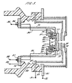
- Figure 3 illustrates a particular structure of ion source and extraction assembly which may be used in an embodiment of the present invention.
- the first, second, third and fourth electrodes forming the front face of the arc chamber of the ion source and the extraction assembly are shown at 70, 71, 72 and 73 respectively.
- the arc chamber of the ion source is illustrated schematically at 74 in reduced size for clarity.
- the front face of the arc chamber forming the first electrode 70 is mounted on a conducting cylinder 75, which is in turn mounted on a conducting flange 76.
- the second electrode 71 has upper and lower parts 77 and 78 which are respectively mounted by pins 79 and 80 on internal flange elements 81 and 82 of the conducting cylinder 75.
- the mounting pins 79 and 80 include insulating segments 83 and 84 within screening bells 85 and 86, so that the parts 77 and 78 are insulated from the cylinder 75 and the front face 70 of the arc chamber 74.
- the pins 79 effectively mount the parts 77 and 78 of the second electrode 71 securely in a predetermined spaced relation with respect to the front face 70 forming the first electrode.
- the third electrode 72 is mounted on a conducting flange 87 which is sandwiched between insulating collars 88 and 89.
- the fourth electrode 73, the shield electrode, is in turn mounted on a further conducting flange 90 which is insulated from the conducting flange 87 by the insulating collar 89.
- Connections to the third and fourth electrodes 72 and 73 may be made via the conducting flanges 87 and 90 at terminals 91 and 92 respectively. Connection to the ion source 74 and the front face 70 forming the first electrode may be made via the flange 76 at a terminal 93. Connections 94 and 95 to the parts 77 and 78 of the second electrode 71 are fed out through insulating feedthroughs 96 and 97 to respective terminals 98 and 99.
- each of electrodes 70, 71, 72 and 73 includes an aperture through which a beam of ions can pass.
- the apertures in the electrodes become progressively wider towards the outermost electrode 73.
Landscapes
- Chemical & Material Sciences (AREA)
- Analytical Chemistry (AREA)
- Physical Vapour Deposition (AREA)
Applications Claiming Priority (3)
| Application Number | Priority Date | Filing Date | Title |
|---|---|---|---|
| US962257 | 1997-10-31 | ||
| US08/962,257 US6060715A (en) | 1997-10-31 | 1997-10-31 | Method and apparatus for ion beam scanning in an ion implanter |
| EP98951570A EP1027718A1 (de) | 1997-10-31 | 1998-10-30 | Ionenstrahlabtastverfahren und vorrichtung in einem ionen-implantationsgerät |
Related Parent Applications (1)
| Application Number | Title | Priority Date | Filing Date |
|---|---|---|---|
| EP98951570A Division EP1027718A1 (de) | 1997-10-31 | 1998-10-30 | Ionenstrahlabtastverfahren und vorrichtung in einem ionen-implantationsgerät |
Publications (2)
| Publication Number | Publication Date |
|---|---|
| EP1235252A2 true EP1235252A2 (de) | 2002-08-28 |
| EP1235252A3 EP1235252A3 (de) | 2003-03-26 |
Family
ID=25505613
Family Applications (2)
| Application Number | Title | Priority Date | Filing Date |
|---|---|---|---|
| EP98951570A Withdrawn EP1027718A1 (de) | 1997-10-31 | 1998-10-30 | Ionenstrahlabtastverfahren und vorrichtung in einem ionen-implantationsgerät |
| EP02076746A Withdrawn EP1235252A3 (de) | 1997-10-31 | 1998-10-30 | Ionenstrahlabtastverfahren und vorrichtung in einem Ionenimplantationsgerät |
Family Applications Before (1)
| Application Number | Title | Priority Date | Filing Date |
|---|---|---|---|
| EP98951570A Withdrawn EP1027718A1 (de) | 1997-10-31 | 1998-10-30 | Ionenstrahlabtastverfahren und vorrichtung in einem ionen-implantationsgerät |
Country Status (4)
| Country | Link |
|---|---|
| US (1) | US6060715A (de) |
| EP (2) | EP1027718A1 (de) |
| JP (1) | JP2001522128A (de) |
| WO (1) | WO1999023685A1 (de) |
Families Citing this family (33)
| Publication number | Priority date | Publication date | Assignee | Title |
|---|---|---|---|---|
| GB2345574A (en) * | 1999-01-05 | 2000-07-12 | Applied Materials Inc | Apparatus and method for monitoring and tuning an ion beam in an ion implantation apparatus |
| WO2001001438A1 (en) * | 1999-06-23 | 2001-01-04 | Applied Materials, Inc. | Ion beam generation apparatus |
| US6489622B1 (en) * | 2000-03-01 | 2002-12-03 | Advanced Ion Beam Technology, Inc. | Apparatus for decelerating ion beams with minimal energy contamination |
| US7106425B1 (en) | 2000-09-20 | 2006-09-12 | Kla-Tencor Technologies Corp. | Methods and systems for determining a presence of defects and a thin film characteristic of a specimen |
| US6673637B2 (en) | 2000-09-20 | 2004-01-06 | Kla-Tencor Technologies | Methods and systems for determining a presence of macro defects and overlay of a specimen |
| US6812045B1 (en) | 2000-09-20 | 2004-11-02 | Kla-Tencor, Inc. | Methods and systems for determining a characteristic of a specimen prior to, during, or subsequent to ion implantation |
| US7130029B2 (en) | 2000-09-20 | 2006-10-31 | Kla-Tencor Technologies Corp. | Methods and systems for determining an adhesion characteristic and a thickness of a specimen |
| US6633831B2 (en) | 2000-09-20 | 2003-10-14 | Kla Tencor Technologies | Methods and systems for determining a critical dimension and a thin film characteristic of a specimen |
| US6919957B2 (en) | 2000-09-20 | 2005-07-19 | Kla-Tencor Technologies Corp. | Methods and systems for determining a critical dimension, a presence of defects, and a thin film characteristic of a specimen |
| US6694284B1 (en) | 2000-09-20 | 2004-02-17 | Kla-Tencor Technologies Corp. | Methods and systems for determining at least four properties of a specimen |
| US7349090B2 (en) | 2000-09-20 | 2008-03-25 | Kla-Tencor Technologies Corp. | Methods and systems for determining a property of a specimen prior to, during, or subsequent to lithography |
| US6782337B2 (en) | 2000-09-20 | 2004-08-24 | Kla-Tencor Technologies Corp. | Methods and systems for determining a critical dimension an a presence of defects on a specimen |
| US6891627B1 (en) | 2000-09-20 | 2005-05-10 | Kla-Tencor Technologies Corp. | Methods and systems for determining a critical dimension and overlay of a specimen |
| WO2002054442A2 (en) * | 2000-12-28 | 2002-07-11 | Proteros, Llc | Ion beam collimating system |
| US20020185607A1 (en) * | 2001-04-03 | 2002-12-12 | Reyes Jaime M. | Ion source filament and method |
| GB2386247B (en) | 2002-01-11 | 2005-09-07 | Applied Materials Inc | Ion beam generator |
| US6627466B1 (en) * | 2002-05-03 | 2003-09-30 | Lsi Logic Corporation | Method and apparatus for detecting backside contamination during fabrication of a semiconductor wafer |
| US6767809B2 (en) * | 2002-11-19 | 2004-07-27 | Silterra Malayisa Sdn. Bhd. | Method of forming ultra shallow junctions |
| US6777696B1 (en) * | 2003-02-21 | 2004-08-17 | Axcelis Technologies, Inc. | Deflecting acceleration/deceleration gap |
| US20050112853A1 (en) * | 2003-11-26 | 2005-05-26 | Raymond Kuzbyt | System and method for non-destructive implantation characterization of quiescent material |
| KR100510559B1 (ko) * | 2003-12-30 | 2005-08-26 | 삼성전자주식회사 | 이온 주입 장비의 매니퓰레이터 어셈블리 |
| US7598505B2 (en) * | 2005-03-08 | 2009-10-06 | Axcelis Technologies, Inc. | Multichannel ion gun |
| CN101322217B (zh) * | 2005-11-15 | 2012-02-29 | 瓦里安半导体设备公司 | 缎带状离子束的成形方法 |
| US7339179B2 (en) * | 2005-11-15 | 2008-03-04 | Varian Semiconductor Equipment Associates, Inc. | Technique for providing a segmented electrostatic lens in an ion implanter |
| US20070164205A1 (en) * | 2006-01-17 | 2007-07-19 | Truche Jean L | Method and apparatus for mass spectrometer diagnostics |
| US7394079B2 (en) * | 2006-01-27 | 2008-07-01 | Varian Semiconductor Equipment Associates, Inc. | Architecture for ribbon ion beam ion implanter system |
| US7675046B2 (en) * | 2006-09-27 | 2010-03-09 | Varian Semiconductor Equipment Associates, Inc | Terminal structure of an ion implanter |
| JP5329050B2 (ja) * | 2007-04-20 | 2013-10-30 | 株式会社Sen | ビーム処理装置 |
| US20090121149A1 (en) * | 2007-11-09 | 2009-05-14 | Varian Semiconductor Equipment Associates, Inc. | Techniques for shaping an ion beam |
| US7767986B2 (en) * | 2008-06-20 | 2010-08-03 | Varian Semiconductor Equipment Associates, Inc. | Method and apparatus for controlling beam current uniformity in an ion implanter |
| US7888653B2 (en) * | 2009-01-02 | 2011-02-15 | Varian Semiconductor Equipment Associates, Inc. | Techniques for independently controlling deflection, deceleration and focus of an ion beam |
| EP2809820A1 (de) * | 2012-02-03 | 2014-12-10 | Seagate Technology LLC | Verfahren zur herstellung von schichten |
| JP6076838B2 (ja) * | 2013-05-31 | 2017-02-08 | 住友重機械イオンテクノロジー株式会社 | 絶縁構造及び絶縁方法 |
Family Cites Families (6)
| Publication number | Priority date | Publication date | Assignee | Title |
|---|---|---|---|---|
| GB1280013A (en) * | 1969-09-05 | 1972-07-05 | Atomic Energy Authority Uk | Improvements in or relating to apparatus bombarding a target with ions |
| US3795833A (en) * | 1972-05-25 | 1974-03-05 | Hughes Aircraft Co | Ion beam deflection system |
| US5389793A (en) * | 1983-08-15 | 1995-02-14 | Applied Materials, Inc. | Apparatus and methods for ion implantation |
| EP0139377B1 (de) * | 1983-08-15 | 1991-03-27 | Applied Materials, Inc. | Vorrichtung und Verfahren zur Ionenimplantation |
| US4580058A (en) * | 1984-03-29 | 1986-04-01 | Zymet, Inc. | Scanning treatment apparatus |
| US4914305A (en) * | 1989-01-04 | 1990-04-03 | Eaton Corporation | Uniform cross section ion beam system |
-
1997
- 1997-10-31 US US08/962,257 patent/US6060715A/en not_active Expired - Lifetime
-
1998
- 1998-10-30 JP JP2000519455A patent/JP2001522128A/ja not_active Withdrawn
- 1998-10-30 EP EP98951570A patent/EP1027718A1/de not_active Withdrawn
- 1998-10-30 WO PCT/GB1998/003248 patent/WO1999023685A1/en not_active Ceased
- 1998-10-30 EP EP02076746A patent/EP1235252A3/de not_active Withdrawn
Also Published As
| Publication number | Publication date |
|---|---|
| JP2001522128A (ja) | 2001-11-13 |
| US6060715A (en) | 2000-05-09 |
| EP1235252A3 (de) | 2003-03-26 |
| EP1027718A1 (de) | 2000-08-16 |
| WO1999023685A1 (en) | 1999-05-14 |
Similar Documents
| Publication | Publication Date | Title |
|---|---|---|
| US6060715A (en) | Method and apparatus for ion beam scanning in an ion implanter | |
| US6130436A (en) | Acceleration and analysis architecture for ion implanter | |
| US5206516A (en) | Low energy, steered ion beam deposition system having high current at low pressure | |
| US6777882B2 (en) | Ion beam generator | |
| EP0501638B1 (de) | Ionenimplantierungsgerät mit verringertem Weg | |
| US6639227B1 (en) | Apparatus and method for charged particle filtering and ion implantation | |
| EP0875918B1 (de) | Elekrostatische Linse mit Beschleunigung und Abbremsung zur variablen Fokussierung und Massenauflösung eines Ionenstrahls in einer Ionenimplantationsanlage | |
| US6559454B1 (en) | Ion beam generation apparatus | |
| KR100479374B1 (ko) | 원추 자기 주사를 사용하는 이온 빔 주입 장치 및 방법 | |
| JP7492516B2 (ja) | イオン源のためのテトロード引出装置 | |
| WO1986007189A1 (en) | Apparatus for scanning a high current ion beam with a constant angle of incidence | |
| CN1809910B (zh) | 离子注入系统中用于等离子体发生的薄磁控管结构 | |
| WO2006014633A2 (en) | Electrostatic lens for ion beams | |
| US5554853A (en) | Producing ion beams suitable for ion implantation and improved ion implantation apparatus and techniques | |
| US6897457B1 (en) | Apparatus and method for monitoring and tuning an ion beam in ion implantation apparatus | |
| JPH11354064A (ja) | イオン注入装置 | |
| EP0066175B1 (de) | Ionenimplantationsvorrichtung | |
| KR20240163667A (ko) | 전환 가능한 분석 자석을 가지는 이중 소스 인젝터 | |
| JPH02260356A (ja) | イオン注入装置における平行走査系 | |
| JPH01252774A (ja) | イオン注入装置 |
Legal Events
| Date | Code | Title | Description |
|---|---|---|---|
| PUAI | Public reference made under article 153(3) epc to a published international application that has entered the european phase |
Free format text: ORIGINAL CODE: 0009012 |
|
| 17P | Request for examination filed |
Effective date: 20020502 |
|
| AC | Divisional application: reference to earlier application |
Ref document number: 1027718 Country of ref document: EP |
|
| AK | Designated contracting states |
Kind code of ref document: A2 Designated state(s): DE GB |
|
| PUAL | Search report despatched |
Free format text: ORIGINAL CODE: 0009013 |
|
| AK | Designated contracting states |
Kind code of ref document: A3 Designated state(s): DE GB Designated state(s): DE GB |
|
| RIC1 | Information provided on ipc code assigned before grant |
Ipc: 7H 01J 37/08 B Ipc: 7H 01J 37/147 B Ipc: 7H 01J 37/317 A |
|
| AKX | Designation fees paid |
Designated state(s): DE GB |
|
| STAA | Information on the status of an ep patent application or granted ep patent |
Free format text: STATUS: THE APPLICATION IS DEEMED TO BE WITHDRAWN |
|
| 18D | Application deemed to be withdrawn |
Effective date: 20030927 |