EP1235470A1 - Agencement de plages de contact pour un panneau à circuit imprimé et procédé de montage de composants sur celui-ci - Google Patents
Agencement de plages de contact pour un panneau à circuit imprimé et procédé de montage de composants sur celui-ci Download PDFInfo
- Publication number
- EP1235470A1 EP1235470A1 EP01107909A EP01107909A EP1235470A1 EP 1235470 A1 EP1235470 A1 EP 1235470A1 EP 01107909 A EP01107909 A EP 01107909A EP 01107909 A EP01107909 A EP 01107909A EP 1235470 A1 EP1235470 A1 EP 1235470A1
- Authority
- EP
- European Patent Office
- Prior art keywords
- sections
- connection
- circuit board
- adjacent
- printed circuit
- Prior art date
- Legal status (The legal status is an assumption and is not a legal conclusion. Google has not performed a legal analysis and makes no representation as to the accuracy of the status listed.)
- Withdrawn
Links
- 238000000034 method Methods 0.000 title claims abstract description 23
- 230000000295 complement effect Effects 0.000 claims abstract description 5
- 229910000679 solder Inorganic materials 0.000 claims description 26
- 238000005476 soldering Methods 0.000 claims description 14
- 238000012216 screening Methods 0.000 claims description 2
- 238000010438 heat treatment Methods 0.000 claims 1
- 230000015572 biosynthetic process Effects 0.000 abstract 1
- 238000011161 development Methods 0.000 description 7
- 230000018109 developmental process Effects 0.000 description 7
- 239000003292 glue Substances 0.000 description 4
- 238000004519 manufacturing process Methods 0.000 description 4
- 239000000853 adhesive Substances 0.000 description 2
- 230000001070 adhesive effect Effects 0.000 description 2
- 238000012545 processing Methods 0.000 description 2
- 239000003990 capacitor Substances 0.000 description 1
- 238000012856 packing Methods 0.000 description 1
- 230000005855 radiation Effects 0.000 description 1
Images
Classifications
-
- H—ELECTRICITY
- H05—ELECTRIC TECHNIQUES NOT OTHERWISE PROVIDED FOR
- H05K—PRINTED CIRCUITS; CASINGS OR CONSTRUCTIONAL DETAILS OF ELECTRIC APPARATUS; MANUFACTURE OF ASSEMBLAGES OF ELECTRICAL COMPONENTS
- H05K1/00—Printed circuits
- H05K1/02—Details
- H05K1/11—Printed elements for providing electric connections to or between printed circuits
- H05K1/111—Pads for surface mounting, e.g. lay-out
-
- H—ELECTRICITY
- H05—ELECTRIC TECHNIQUES NOT OTHERWISE PROVIDED FOR
- H05K—PRINTED CIRCUITS; CASINGS OR CONSTRUCTIONAL DETAILS OF ELECTRIC APPARATUS; MANUFACTURE OF ASSEMBLAGES OF ELECTRICAL COMPONENTS
- H05K1/00—Printed circuits
- H05K1/02—Details
- H05K1/0286—Programmable, customizable or modifiable circuits
- H05K1/0293—Individual printed conductors which are adapted for modification, e.g. fusable or breakable conductors, printed switches
-
- H—ELECTRICITY
- H05—ELECTRIC TECHNIQUES NOT OTHERWISE PROVIDED FOR
- H05K—PRINTED CIRCUITS; CASINGS OR CONSTRUCTIONAL DETAILS OF ELECTRIC APPARATUS; MANUFACTURE OF ASSEMBLAGES OF ELECTRICAL COMPONENTS
- H05K1/00—Printed circuits
- H05K1/02—Details
- H05K1/0286—Programmable, customizable or modifiable circuits
- H05K1/0295—Programmable, customizable or modifiable circuits adapted for choosing between different types or different locations of mounted components
-
- H—ELECTRICITY
- H05—ELECTRIC TECHNIQUES NOT OTHERWISE PROVIDED FOR
- H05K—PRINTED CIRCUITS; CASINGS OR CONSTRUCTIONAL DETAILS OF ELECTRIC APPARATUS; MANUFACTURE OF ASSEMBLAGES OF ELECTRICAL COMPONENTS
- H05K1/00—Printed circuits
- H05K1/02—Details
- H05K1/11—Printed elements for providing electric connections to or between printed circuits
-
- H—ELECTRICITY
- H05—ELECTRIC TECHNIQUES NOT OTHERWISE PROVIDED FOR
- H05K—PRINTED CIRCUITS; CASINGS OR CONSTRUCTIONAL DETAILS OF ELECTRIC APPARATUS; MANUFACTURE OF ASSEMBLAGES OF ELECTRICAL COMPONENTS
- H05K2201/00—Indexing scheme relating to printed circuits covered by H05K1/00
- H05K2201/03—Conductive materials
- H05K2201/0302—Properties and characteristics in general
- H05K2201/0305—Solder used for other purposes than connections between PCB or components, e.g. for filling vias or for programmable patterns
-
- H—ELECTRICITY
- H05—ELECTRIC TECHNIQUES NOT OTHERWISE PROVIDED FOR
- H05K—PRINTED CIRCUITS; CASINGS OR CONSTRUCTIONAL DETAILS OF ELECTRIC APPARATUS; MANUFACTURE OF ASSEMBLAGES OF ELECTRICAL COMPONENTS
- H05K2201/00—Indexing scheme relating to printed circuits covered by H05K1/00
- H05K2201/09—Shape and layout
- H05K2201/09209—Shape and layout details of conductors
- H05K2201/09372—Pads and lands
- H05K2201/09381—Shape of non-curved single flat metallic pad, land or exposed part thereof; Shape of electrode of leadless component
-
- H—ELECTRICITY
- H05—ELECTRIC TECHNIQUES NOT OTHERWISE PROVIDED FOR
- H05K—PRINTED CIRCUITS; CASINGS OR CONSTRUCTIONAL DETAILS OF ELECTRIC APPARATUS; MANUFACTURE OF ASSEMBLAGES OF ELECTRICAL COMPONENTS
- H05K2201/00—Indexing scheme relating to printed circuits covered by H05K1/00
- H05K2201/09—Shape and layout
- H05K2201/09818—Shape or layout details not covered by a single group of H05K2201/09009 - H05K2201/09809
- H05K2201/09954—More mounting possibilities, e.g. on same place of PCB, or by using different sets of edge pads
-
- H—ELECTRICITY
- H05—ELECTRIC TECHNIQUES NOT OTHERWISE PROVIDED FOR
- H05K—PRINTED CIRCUITS; CASINGS OR CONSTRUCTIONAL DETAILS OF ELECTRIC APPARATUS; MANUFACTURE OF ASSEMBLAGES OF ELECTRICAL COMPONENTS
- H05K2201/00—Indexing scheme relating to printed circuits covered by H05K1/00
- H05K2201/10—Details of components or other objects attached to or integrated in a printed circuit board
- H05K2201/10613—Details of electrical connections of non-printed components, e.g. special leads
- H05K2201/10621—Components characterised by their electrical contacts
- H05K2201/10636—Leadless chip, e.g. chip capacitor or resistor
-
- H—ELECTRICITY
- H05—ELECTRIC TECHNIQUES NOT OTHERWISE PROVIDED FOR
- H05K—PRINTED CIRCUITS; CASINGS OR CONSTRUCTIONAL DETAILS OF ELECTRIC APPARATUS; MANUFACTURE OF ASSEMBLAGES OF ELECTRICAL COMPONENTS
- H05K2203/00—Indexing scheme relating to apparatus or processes for manufacturing printed circuits covered by H05K3/00
- H05K2203/17—Post-manufacturing processes
- H05K2203/173—Adding connections between adjacent pads or conductors, e.g. for modifying or repairing
-
- Y—GENERAL TAGGING OF NEW TECHNOLOGICAL DEVELOPMENTS; GENERAL TAGGING OF CROSS-SECTIONAL TECHNOLOGIES SPANNING OVER SEVERAL SECTIONS OF THE IPC; TECHNICAL SUBJECTS COVERED BY FORMER USPC CROSS-REFERENCE ART COLLECTIONS [XRACs] AND DIGESTS
- Y02—TECHNOLOGIES OR APPLICATIONS FOR MITIGATION OR ADAPTATION AGAINST CLIMATE CHANGE
- Y02P—CLIMATE CHANGE MITIGATION TECHNOLOGIES IN THE PRODUCTION OR PROCESSING OF GOODS
- Y02P70/00—Climate change mitigation technologies in the production process for final industrial or consumer products
- Y02P70/50—Manufacturing or production processes characterised by the final manufactured product
Definitions
- the present invention relates to a connection device for a printed circuit board and method for assembling the same.
- SMD Surface Mounted Devices
- electrical components e.g. Resistors, capacitors, Diodes, transistors and integrated circuits the surface of printed circuit boards.
- a Solder for example a solder paste, or non-conductive Adhesive fixed and then soldered to connection devices.
- Miniature components are complementary to this, for example trained connection surfaces necessary. Such smaller components result in a higher packing density and the corresponding Printed circuit boards can be made smaller.
- Printed circuit board variants have to be created for different applications that also require different equipment. Often, several circuit boards with different Executions used.
- connection devices for a circuit board with of making bridge connections on combination circuit boards without additional components component glue and can be carried out without additional processing operations.
- each connection device arranged on the circuit board at least one component mounting section and at least one connecting section for at least one has adjacent connection device, wherein adjacent Connection sections to form an easily bridgeable Gaps are matched to each other.
- the connecting sections Adjacent connection devices complementary to each other Forms on.
- a good connection is made at Guaranteed application of a solder.
- connection sections of adjacent connection devices in each case non-contact comb-shaped. This makes one geometric ensures simple and effective connection and Manufacturing costs can be kept low.
- the component assembly sections are neighboring connection facilities opposite and the associated connecting sections between the corresponding connection devices arranged. This ensures that, for example in the case of wave or wave soldering, the connecting sections then be protected from a soldering process when a component on the corresponding component assembly sections is attached and thus protecting the connecting sections covers.
- application is carried out the components on the circuit board and for manufacturing the solder bridges at the desired locations, for example the so-called reflow process, the dip, wave or wave soldering process used.
- the so-called Reflow process for applying the solder to both the component mounting sections as well as on the connecting sections used at least one screening device. It is a sieve device, which the recesses for applying a solder to the desired one Places.
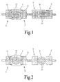
- connection facilities 3, 3 'each have a component mounting section 31 and a connecting section 32 are the connecting sections 32 of two adjacent connection devices 3, 3 'formed such that they according to the first embodiment of the present invention intermesh comb-like, an easily bridgeable Gap 6, i. H. with a predetermined slight width, is provided for a contactless structure. This ensures that the connection sections before a soldering process 32 of two adjacent connection devices 3, 3 ' do not contact.
- Components 7 to be assembled can be placed on the component assembly sections 31 two adjacent connection devices 3, 3 'are attached so that they are complete cover the connecting portions 32 protectively.
- Such a attached component 7 is shown in Fig. 1 schematically by the dashed line indicated.
- Fig. 2 shows connection devices 3, 3 'according to a second Embodiment of the present invention. Not explained Components or functions are analogous to the first Embodiment and therefore need no further explanation.
- connection sections 32 of two adjacent connection devices 3, 3 ' formed such that the connecting section the connection device 3 'circular and the correspondingly assigned connection section 32 of the connection device 3 is c-shaped, being the Connection section of the connection device 3 'contactless encloses, which in turn creates a contactless structure the gap 6 can be easily bridged.
- connection portions 32 of adjacent connection devices 3, 3 'to form an easily bridgeable Gaps 6 are matched to each other. This ensures that by applying a solder and one subsequent soldering process an electrical contact without use an additional component is created.
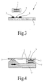
- the components to be assembled SMD components 7 such as glue 9 attached to the circuit board 2, that they, as in Fig. 1st can be seen on the component mounting sections 31 of the respective connection devices 3, 3 'are attached and cover the connecting portions 32 protectively.
- the contact points of the components 7 with the component mounting sections 31 by placing it in a solder bath introduced to form a "wave" and thus together soldered.
- a solder short circuit is caused by applied components 7 of the connecting sections 32 underneath, as seen in Fig. 4 prevented.
- the connecting sections 32 connected by a solder bridge the were not equipped with a component.
- the present invention proceeded as follows. First of all a solder through, for example, a sieve onto the component mounting sections 31 applied with a component 7 or solder bridges to be equipped.
- the components to be assembled are in the Solder paste on the corresponding component assembly sections 31 used and for example by infrared radiation, Hotplate or hot air fused, one Solder connection between the components 7 and the corresponding ones Component placement sections 31 and between the as Adjacent connecting sections 32 serving for soldering bridges will be produced.
- connection sections are more adjacent Connection facilities conceivable.
- Soldering processes mentioned here can only be seen as an example.
Landscapes
- Engineering & Computer Science (AREA)
- Microelectronics & Electronic Packaging (AREA)
- Combinations Of Printed Boards (AREA)
- Electric Connection Of Electric Components To Printed Circuits (AREA)
Applications Claiming Priority (2)
| Application Number | Priority Date | Filing Date | Title |
|---|---|---|---|
| DE10108780A DE10108780A1 (de) | 2001-02-23 | 2001-02-23 | Anschlusseinrichtung für eine Leiterplatte und Verfahren zum Bestücken derselben |
| DE10108780 | 2001-02-23 |
Publications (1)
| Publication Number | Publication Date |
|---|---|
| EP1235470A1 true EP1235470A1 (fr) | 2002-08-28 |
Family
ID=7675262
Family Applications (1)
| Application Number | Title | Priority Date | Filing Date |
|---|---|---|---|
| EP01107909A Withdrawn EP1235470A1 (fr) | 2001-02-23 | 2001-03-28 | Agencement de plages de contact pour un panneau à circuit imprimé et procédé de montage de composants sur celui-ci |
Country Status (2)
| Country | Link |
|---|---|
| EP (1) | EP1235470A1 (fr) |
| DE (1) | DE10108780A1 (fr) |
Cited By (1)
| Publication number | Priority date | Publication date | Assignee | Title |
|---|---|---|---|---|
| CN112566366A (zh) * | 2019-09-25 | 2021-03-26 | 崧虹科技股份有限公司 | 具有切换开关的焊接点 |
Families Citing this family (2)
| Publication number | Priority date | Publication date | Assignee | Title |
|---|---|---|---|---|
| DE10344631B4 (de) * | 2003-09-25 | 2013-12-24 | Robert Bosch Gmbh | Elektronische Schaltungsanordnung |
| DE202010008479U1 (de) * | 2010-09-08 | 2011-12-09 | Zumtobel Lighting Gmbh | Leiterplatte zum Bestücken mit Leuchtkörpern |
Citations (6)
| Publication number | Priority date | Publication date | Assignee | Title |
|---|---|---|---|---|
| DE2111502A1 (de) * | 1971-03-10 | 1972-09-21 | Siemens Ag | Verfahren zum Bestuecken von Bauplatten mit vorzugsweise elektrischen Bauteilen |
| US4379318A (en) * | 1979-09-21 | 1983-04-05 | Nissan Motor Company, Limited | Overcurrent safety construction for a printed circuit board |
| US4982892A (en) * | 1989-11-09 | 1991-01-08 | International Business Machines Corporation | Solder interconnects for selective line coupling |
| US5303122A (en) * | 1991-10-31 | 1994-04-12 | Ford Motor Company | Printed circuit board having a commonized mounting pad which different sized surface mounted devices can be mounted |
| JPH0786729A (ja) * | 1993-09-09 | 1995-03-31 | Ibiden Co Ltd | プリント配線板におけるジャンパーランドの接続構造及びジャンパーランドの接続方法 |
| JPH08279661A (ja) * | 1995-04-10 | 1996-10-22 | Matsushita Electric Ind Co Ltd | プリント基板 |
-
2001
- 2001-02-23 DE DE10108780A patent/DE10108780A1/de not_active Withdrawn
- 2001-03-28 EP EP01107909A patent/EP1235470A1/fr not_active Withdrawn
Patent Citations (6)
| Publication number | Priority date | Publication date | Assignee | Title |
|---|---|---|---|---|
| DE2111502A1 (de) * | 1971-03-10 | 1972-09-21 | Siemens Ag | Verfahren zum Bestuecken von Bauplatten mit vorzugsweise elektrischen Bauteilen |
| US4379318A (en) * | 1979-09-21 | 1983-04-05 | Nissan Motor Company, Limited | Overcurrent safety construction for a printed circuit board |
| US4982892A (en) * | 1989-11-09 | 1991-01-08 | International Business Machines Corporation | Solder interconnects for selective line coupling |
| US5303122A (en) * | 1991-10-31 | 1994-04-12 | Ford Motor Company | Printed circuit board having a commonized mounting pad which different sized surface mounted devices can be mounted |
| JPH0786729A (ja) * | 1993-09-09 | 1995-03-31 | Ibiden Co Ltd | プリント配線板におけるジャンパーランドの接続構造及びジャンパーランドの接続方法 |
| JPH08279661A (ja) * | 1995-04-10 | 1996-10-22 | Matsushita Electric Ind Co Ltd | プリント基板 |
Non-Patent Citations (3)
| Title |
|---|
| PARLA A ET AL: "SOLDER INTERCONNECTIONS FOR SMT SELECTIVE LINE COUPLING", IEEE TRANSACTIONS ON COMPONENTS,HYBRIDS,AND MANUFACTURING TECHNOLOGY, IEEE INC. NEW YORK, US, vol. 14, no. 4, 1 December 1991 (1991-12-01), pages 738 - 743, XP000274247, ISSN: 0148-6411 * |
| PATENT ABSTRACTS OF JAPAN vol. 1995, no. 06 31 July 1995 (1995-07-31) * |
| PATENT ABSTRACTS OF JAPAN vol. 1997, no. 02 28 February 1997 (1997-02-28) * |
Cited By (1)
| Publication number | Priority date | Publication date | Assignee | Title |
|---|---|---|---|---|
| CN112566366A (zh) * | 2019-09-25 | 2021-03-26 | 崧虹科技股份有限公司 | 具有切换开关的焊接点 |
Also Published As
| Publication number | Publication date |
|---|---|
| DE10108780A1 (de) | 2002-09-05 |
Similar Documents
| Publication | Publication Date | Title |
|---|---|---|
| EP0762817A1 (fr) | Blindage pour des plaquettes de circuit | |
| DE19651122C2 (de) | Halbleiterbauelement mit einem Halbleiterchip und einer Leiterplatte | |
| DE3535923C2 (fr) | ||
| DE3607049C2 (fr) | ||
| DE2852753B2 (de) | Verfahren zum Befestigen von Bauelementen mit flächigen Anschlußkontakten auf einer Leiterplatte | |
| WO2002100140A2 (fr) | Carte de circuits imprimes pourvue d'au moins un composant electronique | |
| DE60128537T2 (de) | Zusammenbau zur verbindung von mindestens zwei gedruckten schaltungen | |
| EP1665914A1 (fr) | Carte de circuits imprimes comprenant un dispositif de maintien concu pour maintenir des composants electroniques cables, procede pour produire une telle carte de circuits imprimes et son utilisation dans un four a braser | |
| DE3501710C2 (fr) | ||
| EP0613331B1 (fr) | Méthode d'attachement d'un circuit hybride sur un circuit imprimé | |
| WO2002093992A1 (fr) | Carte de circuits imprimes sur laquelle un connecteur femelle est monte | |
| DE3138987C2 (de) | Einrichtung zum Verhindern von Beschädigungen von Bausteinen bzw. Leiterbahnen auf einer Leiterplatte | |
| EP1606982B1 (fr) | Procede de connexion electrique et mecanique de deux cartes a circuits imprimes | |
| DE112015003374T5 (de) | Schaltungsanordnung | |
| EP1235470A1 (fr) | Agencement de plages de contact pour un panneau à circuit imprimé et procédé de montage de composants sur celui-ci | |
| DE102012112546A1 (de) | Verfahren zur Herstellung von mischbestückten Leiterplatten | |
| DE19512272C2 (de) | Verfahren zur Herstellung einer mehrschichtigen Leiterplatte für ein Chassis eines unterhaltungselektronischen Gerätes und Leiterplatte hergestellt nach diesem Verfahren | |
| DE3523646A1 (de) | Mehrschichtige schaltungsplatine mit plattierten durchgangsbohrungen | |
| DE69904424T2 (de) | Aufbau und Verfahren zum Montieren einer elektronischen Einheit auf eine gedruckte Schaltungsplatte | |
| EP0968629B1 (fr) | Module plat et procede de montage ulterieur de composants supplementaires sur une carte imprimee | |
| EP0304902B1 (fr) | Dispositif utilisé pour la modification et/ou la réparation des voies conductrices portées par un panneau comportant des composants montés en surface | |
| DE4208594A1 (de) | Verfahren zur herstellung einer elektrischen, vorgefertigten baueinheit und deren befestigung auf einer leiterplatte | |
| EP1111974B1 (fr) | Procédé de fabrication d'une connexion à soudage | |
| DE29617021U1 (de) | Leiterplatte | |
| DE2314566A1 (de) | Schaltkarte und verfahren zur herstellung der schaltkarte |
Legal Events
| Date | Code | Title | Description |
|---|---|---|---|
| PUAI | Public reference made under article 153(3) epc to a published international application that has entered the european phase |
Free format text: ORIGINAL CODE: 0009012 |
|
| AK | Designated contracting states |
Kind code of ref document: A1 Designated state(s): AT BE CH CY DE DK ES FI FR GB GR IE IT LI LU MC NL PT SE TR |
|
| AX | Request for extension of the european patent |
Free format text: AL;LT;LV;MK;RO;SI |
|
| 17P | Request for examination filed |
Effective date: 20021202 |
|
| AKX | Designation fees paid |
Designated state(s): DE FR |
|
| STAA | Information on the status of an ep patent application or granted ep patent |
Free format text: STATUS: THE APPLICATION HAS BEEN WITHDRAWN |
|
| 18W | Application withdrawn |
Effective date: 20060104 |