EP1238456B1 - Circuit de sortie equilibre et flottant - Google Patents
Circuit de sortie equilibre et flottant Download PDFInfo
- Publication number
- EP1238456B1 EP1238456B1 EP00993061A EP00993061A EP1238456B1 EP 1238456 B1 EP1238456 B1 EP 1238456B1 EP 00993061 A EP00993061 A EP 00993061A EP 00993061 A EP00993061 A EP 00993061A EP 1238456 B1 EP1238456 B1 EP 1238456B1
- Authority
- EP
- European Patent Office
- Prior art keywords
- output
- differential
- transconductance amplifier
- voltage
- section
- Prior art date
- Legal status (The legal status is an assumption and is not a legal conclusion. Google has not performed a legal analysis and makes no representation as to the accuracy of the status listed.)
- Expired - Lifetime
Links
Images





Classifications
-
- H—ELECTRICITY
- H03—ELECTRONIC CIRCUITRY
- H03F—AMPLIFIERS
- H03F3/00—Amplifiers with only discharge tubes or only semiconductor devices as amplifying elements
- H03F3/45—Differential amplifiers
- H03F3/45071—Differential amplifiers with semiconductor devices only
- H03F3/45479—Differential amplifiers with semiconductor devices only characterised by the way of common mode signal rejection
- H03F3/45484—Differential amplifiers with semiconductor devices only characterised by the way of common mode signal rejection in differential amplifiers with bipolar transistors as the active amplifying circuit
- H03F3/45488—Differential amplifiers with semiconductor devices only characterised by the way of common mode signal rejection in differential amplifiers with bipolar transistors as the active amplifying circuit by using feedback means
- H03F3/45493—Measuring at the loading circuit of the differential amplifier
- H03F3/45506—Controlling the active amplifying circuit of the differential amplifier
-
- H—ELECTRICITY
- H03—ELECTRONIC CIRCUITRY
- H03F—AMPLIFIERS
- H03F3/00—Amplifiers with only discharge tubes or only semiconductor devices as amplifying elements
- H03F3/45—Differential amplifiers
- H03F3/45071—Differential amplifiers with semiconductor devices only
- H03F3/45479—Differential amplifiers with semiconductor devices only characterised by the way of common mode signal rejection
- H03F3/45484—Differential amplifiers with semiconductor devices only characterised by the way of common mode signal rejection in differential amplifiers with bipolar transistors as the active amplifying circuit
- H03F3/45596—Differential amplifiers with semiconductor devices only characterised by the way of common mode signal rejection in differential amplifiers with bipolar transistors as the active amplifying circuit by offset reduction
- H03F3/45618—Differential amplifiers with semiconductor devices only characterised by the way of common mode signal rejection in differential amplifiers with bipolar transistors as the active amplifying circuit by offset reduction by using balancing means
-
- H—ELECTRICITY
- H03—ELECTRONIC CIRCUITRY
- H03F—AMPLIFIERS
- H03F3/00—Amplifiers with only discharge tubes or only semiconductor devices as amplifying elements
- H03F3/45—Differential amplifiers
- H03F3/45071—Differential amplifiers with semiconductor devices only
- H03F3/45479—Differential amplifiers with semiconductor devices only characterised by the way of common mode signal rejection
- H03F3/45928—Differential amplifiers with semiconductor devices only characterised by the way of common mode signal rejection using IC blocks as the active amplifying circuit
- H03F3/45968—Differential amplifiers with semiconductor devices only characterised by the way of common mode signal rejection using IC blocks as the active amplifying circuit by offset reduction
- H03F3/45991—Differential amplifiers with semiconductor devices only characterised by the way of common mode signal rejection using IC blocks as the active amplifying circuit by offset reduction by using balancing means
Definitions
- the present application relates to a floating, balanced output circuits, and more specifically to an improved floating, balanced output circuit that maintains control of the common-mode output current in both output legs of the circuit even when the differential voltage output is clipped and the circuit is driving a ground-referred load.
- the differential output impedance is substantially determined by the sum of output resistances R O1 , and R O2 , as negative feedback around the operational amplifiers OA1 and OA2 substantially reduces their internal closed-loop output impedances.
- R O1 and R O2 are typically between 10 and 100 ohms in order to keep the differential output impedance relatively low.
- the common-mode output impedance is quite high, and can be infinite if the ratios of the resistances labeled R and 2R in the schematic are precisely maintained. It should be noted that mismatches in these resistor ratios can either reduce the common-mode output impedance if the mismatches are in one direction, or can lead to instability if they are in the other direction. This requirement for precise resistor-ratio matching is a drawback to this circuit.
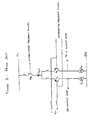
- Its output current will be the output voltage divided by the load resistance. What is not as obvious is that, while clipping is occurring, the output current of the grounded OUT- output will be quite high, typically limited only by any protective current limiting circuit in the opamp, or by the maximum opamp output voltage divided by the value of the 10-to-100 ohm output resistor. This current must flow through an indeterminate path through the ground structure of the load device to return to the output stage, which can lead to disturbances on the audio waveform that are more audible than simple clipping.
- Strahm's circuit includes separate feedback loops for differential and common-mode output signals.
- the differential loop is configured to force the differential output voltage to substantially equal the input voltage multiplied by some desired gain
- the common-mode feedback loop is configured to force the two output terminal currents to be equal and opposite. This at least opens up the possibility of preventing the clipping behavior and the audio waveform disturbances described above. Also, as described in the Strahm patent, precise resistor ratios are not necessary to maintain stability of the circuit.
- the common-mode feedback loop In order to prevent a grounded output of such a circuit from going into current limiting when the active output is driven into voltage clipping, the common-mode feedback loop must remain active even though the differential feedback loop is disabled.
- the integrated circuit device manufactured by the assignee (Audio Teknology Inc.) based on the Strahm patent is implemented in a way that does not preserve the functionality of the common-mode feedback loop when the differential feedback loop is broken due to voltage clipping into a grounded load.
- a differential pair of transistors, Q 1 and Q 2 accept the input signal and the differential feedback signal.
- Transistor Q 3 provides the tail current I tail for the differential pair.
- Q 3 is controlled by the common-mode feedback signal.
- the common-mode feedback signal is derived by sensing the sum of the output currents from the device, as described in the Strahm patent.
- the common-mode output voltage is adjusted via feedback through I tail until the two device output currents sum to nearly zero, and, are thus nearly equal and opposite.
- voltage clipping occurs at either amplifier output, one of Q 1 or Q 2 will saturate while the other will be cut off. If the circuit is driving a ground-referred load from the output amplifier that is driven by the cutoff transistor, then there is no way for Q 3 to affect the output voltage and common-mode feedback is also disabled. Without common-mode feedback to maintain control over the output currents, the grounded output amplifier conducts as much current as permitted by other aspects of the amplifier design, such as protective current limiting.
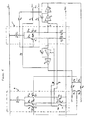
- FIG. 4 shows a schematic drawing of one embodiment of an improved circuit that uses separate differential and common-mode feedback loops to emulate a floating voltage source and controls the output common-mode current under clipping conditions while driving a ground-referred load.
- This transconductance amplifier along with identical inverting high-gain voltage amplifiers 2 and 3, identical buffer amplifiers 4 and 5, and identical compensation capacitors 6 and 7 form a two-stage fully-differential operational amplifier.
- Resistors R 1 and R 2 are connected from the input voltage terminals IN+ and IN-, respectively, to the non-inverting and inverting terminals of transconductance amplifier 1, respectively.
- Resistors R 1 and R 4 are connected from the outputs of buffer amplifiers 4 and 5, respectively, to the non-inverting and inverting inputs of transconductance amplifier 1, respectively, to provide differential negative feedback.
- a cld R 4 R 1
- output currents i 3 and i 4 respectively sum with the output currents i 2 and i 1 of transconductance amplifier 1. Note that the output currents i 3 and i 4 from transconductance amplifier 8 will cause both output voltages (V out+ and V out- ) to move in the same direction, while the output currents i 1 and i 2 from transconductance amplifier 1 will cause the two output voltages ( v out + and v out -) to move in opposite directions.
- Resistors R 9 and R 10 are used to sense the individual output currents, and preferably are of equal value between about 10 and about 100 ohms in order to maintain low differential output impedance, although the values can be outside this range.
- Resistors R 11 and R 12 serve to establish a minimum common-mode load for the circuit, and are preferably between about 1 k ⁇ and about 100 k ⁇ , although the values can be outside this range.
- transconductance amplifier 8 and voltage amplifiers 2 and 3 will tend to minimize the differential voltage at the transconductance amplifier's inputs via negative feedback. This will then tend to minimize the common-mode output current, leaving only differential (equal and opposite) currents.
- Both transconductance amplifiers must be designed to have a maximum possible output current that is achieved when the input voltage exceeds a predefined level. (This is a natural consequence of the preferred implementations, as will be illustrated below).
- the maximum output currents from transconductance amplifier 8 must be made greater than the maximum output currents from transconductance amplifier 1.
- R 11 is a short circuit, such that R 12 serves as a ground-referred load, and that the input voltage v in is sufficiently positive to drive v 2 to the maximum possible positive voltage allowed by the circuit power supplies.
- the negative feedback path via R 4 is now broken, as the voltage v 2 no longer responds to any change in the input voltage.
- i 1 and i 2 will be at their maximum possible values (in opposite directions). Current i 1 will tend to drive voltage v 1 negative, and, if left unchecked, will cause a large current to flow through low-valued resistor R 9 . However, if transconductance amplifier 8 has sufficient output current capability to sink the maximum value of i 1 , then the common-mode feedback loop will act to minimize the common-mode output current. Under these conditions, i 4 will be substantially equal to - i 1 , and i out- will be substantially equal to -i out + .
- output stages 9 and 10 consisting of voltage amplifiers 2 and 3, buffer stages 4 and 5, and compensation capacitors 6 and 7 may take many preferred forms without departing from the scope of the invention.
- voltage amplifiers 2 and 3 may consist of current-source-loaded common emitter amplifiers
- buffer amplifiers 4 and 5 may consist of complementary common-collector amplifiers.
- Other devices, such as MOS transistors, could also be substituted with no loss of essential functionality.
- differential feedback resistors R 3 and R 4 could alternately be connected directly to the OUT+ and OUT- terminals, rather than to the outputs of buffer amplifiers 4 and 5. Such an arrangement would result in lower differential output impedance, but would require more elaborate frequency compensation in order to maintain stability into capacitive loads.
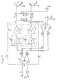
- transconductance amplifier 1 is shown in Figure 5 .
- This structure comprises differential pair transistors Q 1 and Q 2 , current sources I 1 , I 2 , and I 3 and optional equal-valued emitter degeneration resistors R 13 and R 14 .
- the differential input to the transconductance amplifier is applied to the bases of Q 1 and Q 2 .
- the differential output currents are taken from the collectors of Q 1 and Q 2 .
- the values of current sources I 2 and I 3 are each equal to one half of the value of current source I 1 . In this case, the maximum current available in either direction from the collectors of Q 1 and Q 2 is equal to I 1 /2.
- transconductance amplifier 8 is also shown in Figure 5 . It comprises transistors Q 3 , through Q 8 , current source I 4 , and optional emitter degeneration resistors R 15 through R 17 .
- transistor Q 3 has an emitter area twice that of Q 4 and Q 5 .
- the value emitter degeneration resistor R 17 is half the value of identically- valued resistors R 15 and R 16 .
- transistor Q 6 has an emitter area twice that of transistors Q 7 and Q 8 .
- the collector current of Q 6 will be mirrored to the collectors of Q 7 and Q 8 with a gain of 0.5, such that each will operate at a collector current equal to one half of Q 6 's collector current.
- the differential input voltage to transconductance amplifier 8 is applied between the base of transistor Q 3 and the common bases of transistors Q 4 and Q 5 . Identical output currents are taken from the collectors of Q 7 and Q 8 .
- the maximum output current available in either direction from the collectors of Q 4 and Q 5 is equal to one half the value of current source I 4 .
- current source I 4 should be made greater in value than current source I 1 in order to ensure that the common-mode feedback loop will remain active after the differential feedback loop is disabled by clipping.
- transistors Q 7 and Q 8 are sinking collector currents equal to at least I 1 /2, or transistors Q 4 and Q 5 are sourcing collector currents equal to at least I 1 /2.
- a current imbalance equal to the value of current source I 1 will exist between the collector current of Q 3 and the sum of the collector currents of Q 4 and Q 5 .
- This current imbalance will cause an input offset voltage (in addition to that caused by random transistor and resistor mismatches) at the inputs of transconductance amplifier 8 equal to I 1 /g m2 .
- transconductance amplifier 8 This additional input offset voltage will degrade the matching of the magnitudes of the currents in resistors R 9 and R 10 under the aforementioned conditions. If this degradation of performance is unacceptable, an additional gain stage can be added to transconductance amplifier 8 as illustrated in Figure 6 .
- Differential pair transistors Q 9 and Q 10 , optional identical emitter degeneration transistors R 18 and R 19 , current mirror transistors Q 11 and Q 12 , and current source I 5 make up a differential amplifier with a single-ended current output.
- the input voltage to transconductance amplifier 8 is applied between the bases of Q 9 and Q 10 .
- the output current from the collectors of Q 12 and Q 10 is applied to the base of Q 5 of the previously described differential-input, dual-output transconductance amplifier.
- the common bases of Q 3 and Q 4 are tied to an appropriate bias voltage source, preferably far enough below Vcc to ensure proper operation of current source I 4 and transistors Q 3 through Q 5 .
- the dual output currents are taken from the collectors of Q 7 and Q 8 as described above. With this modification to dual-output transconductance amplifier 8, the additional offset voltage created between the base of Q 5 and the common bases of Q 3 and Q 4 when the differential feedback loop is disabled due to clipping is reduced by the gain of differential amplifier stage 11. This results in very little change in input offset voltage at the bases of Q 9 and Q 10 .
- the functions of the circuits above can be implemented in different ways without departing from the scope of the invention.
- the current mirrors composed of Q 6 through Q 8 and Q 11 through Q 12 could be any of a number of improved current mirrors known in the art such as the Wilson current mirror, the cascoded current mirror, or the emitter-follower-augmented current mirror.
- each mirror could have emitter degeneration resistors added to increase the output impedance.
- the differential inputs of transconductance amplifiers 1 and 8 could have emitter follower buffers, and/or bias current cancellation circuitry added to minimize input bias current.
- all of the circuits could be implemented with a different transistor technology, such as MOS transistors.
- capacitor C 1 is inserted between the junction of resistors R 7 and R 8 and the inverting input of transconductance amplifier 8.
- Resistor R 20 is added from the inverting input of transconductance amplifier 8 to ground.
- R 20 is preferably chosen to be large enough in value so as not to significantly load R 7 and R 8 , preferably, although not necessarily 1 M ⁇ or larger if R 5 through R 8 are all about or within a small range of 10 k ⁇ .
- C 1 is chosen so that the high-pass filter formed by C 1 and R 20 has a pole frequency substantially lower than the operational frequencies of interest.
- the common-mode feedback loop will minimize the output common-mode current, forcing equal and opposite currents in R 9 and R 10 .
- the common-mode feedback loop will tend to force the junction of R 5 and R 6 (and thus the output common-mode voltage) to the ground potential, plus or minus any input offset voltage at transconductance amplifier 8's inputs.
- One of the primary applications for floating, balanced output circuits in the professional audio industry is to drive audio signals over cables of up to 1000 feet long. Such cables represent a reactive load on the circuit, with resonant frequencies that may coincide with the unity-gain frequency of the common-mode feedback loop. Such resonances can cause peaks in the loop transmission that will compromise the stability of the loop.
- the common-mode feedback loop can be isolated from these loading effects with the addition of C 2 , also shown in Figure 7 .
- C 2 is preferably chosen so that the lowpass filter that it forms with the parallel combination of R 7 and R 8 is substantially higher than the operation frequencies of interest, but below the unity-gain crossover frequency of the common-mode feedback loop.
- C 2 is equal to about 10 pF.
- C 2 will shunt the inverting input of transconductance amplifier 8 to ground, isolating it from the response peaks due to resonant loads.
- Figure 8 illustrates an alternative and preferred method of minimizing the output common-mode voltage.
- Capacitor C 3 is inserted between the OUT- terminal and resistor R 7 .
- capacitor C 4 is inserted between the OUT+ terminal and resistor R 8 .
- Resistor R 21 is added from the junction of C 3 and R 7 to ground
- resistor R 22 is added from the junction of C 4 and R 8 to ground.
- C 3 and C 4 are each about 10 ⁇ F
- R 21 and R 22 are each about 20 k ⁇ .
- this circuit will minimize the common-mode output current in the audio band, but force the output common-mode voltage to the ground potential at DC.
- the circuit in Figure 8 will maintain a superior match between the output current magnitudes when driving a ground referred load compared with the circuit in Figure 7 . This is due to the absence of any loading on R 7 and R 8 . However, this comes at the expense of an additional capacitor and an additional resistor.
Landscapes
- Engineering & Computer Science (AREA)
- Power Engineering (AREA)
- Amplifiers (AREA)
- Networks Using Active Elements (AREA)
- Circuits Of Receivers In General (AREA)
- Stereo-Broadcasting Methods (AREA)
- Valve Device For Special Equipments (AREA)
Claims (20)
- Circuit à sortie équilibrée flottante destiné à fournir une tension de sortie différentielle en réponse à une tension d'entrée, avec une impédance de sortie différentielle relativement basse et une impédance de sortie de mode commun relativement élevée, comprenant :une première section d'amplificateur de transconductance (1) destinée à fournir une paire différentielle de courants de sortie (i1, i2) en réponse à la tension d'entrée, les courants (i1, i2) étant d'intensités globalement identiques et de polarités opposées, et une section suivante (9) connectée de manière à générer un signal de sortie en réponse à la paire de courants de sortie du premier amplificateur de transconductance,une configuration de boucle de rétroaction différentielle (R3, R4) connectée autour de la première section d'amplificateur de transconductance (1) de manière à fournir une rétroaction négative différentielle, etune configuration de boucle de rétroaction de mode commun comprenant une deuxième section d'amplificateur de transconductance (8) connectée autour de la section suivante (9) de manière à ajouter respectivement une paire de courants de sortie globalement adaptés (i3, i4) aux courants de sortie du premier étage d'amplificateur de transconductance (1) en réponse au signal de sortie,dans lequel les premier et deuxième amplificateurs de transconductance (1, 8) sont conçus de sorte que la configuration de boucle de rétroaction de mode commun reste active lorsque la configuration de boucle de rétroaction différentielle a été inhibée en raison de l'écrêtage lorsque la tension d'entrée dépasse un niveau prédéfini.
- Circuit selon la revendication 1, dans lequel la section suivante comprend une section intermédiaire (9) connectée de manière à générer une tension différentielle intermédiaire (V1, V2) en réponse à la paire de courants de sortie (i1, i2) du premier amplificateur de transconductance (1), le circuit comprenant en outre une section de sortie (R9, R10) destinée à générer une tension de sortie différentielle (Vout) en réponse à la tension différentielle intermédiaire (V1, V2).
- Circuit selon la revendication 2, dans lequel la configuration de boucle de rétroaction différentielle (R3, R4) est connectée autour de la première section d'amplificateur de transconductance (1) et de la section intermédiaire (9) de manière à fournir une rétroaction négative différentielle en réponse à la tension différentielle intermédiaire (V1, V2), et la deuxième section d'amplificateur de transconductance (8) est connectée autour de la section intermédiaire (9) de manière à ajouter respectivement une paire de courants de sortie globalement adaptés (i3, i4) aux courants de sortie (i1, i2) du premier étage d'amplificateur de transconductance (1) en réponse au courant de mode commun.
- Circuit selon la revendication 2 ou 3, comprenant en outre un amplificateur opérationnel totalement différentiel comprenant le premier amplificateur de transconductance (1) et la section intermédiaire (9).
- Circuit selon l'une quelconque des revendications 1 à 4, dans lequel les intensités des courants de sortie maximaux provenant du deuxième amplificateur de transconductance (8) sont supérieures aux intensités des courants de sortie maximaux provenant du premier amplificateur de transconductance (1).
- Circuit selon l'une quelconque des revendications précédentes, comprenant en outre une entrée (R1, R2) reliée au premier amplificateur de transconductance (1) configurée pour recevoir une tension d'entrée différentielle (Vin).
- Circuit selon l'une quelconque des revendications 1 à 4, comprenant en outre une entrée (R1, R2) reliée au premier amplificateur de transconductance (1) configurée pour recevoir une tension d'entrée asymétrique.
- Circuit selon l'une quelconque des revendications 1 à 7, dans lequel la configuration de boucle de rétroaction de mode commun comprend une section de détection de courant (R9, R10) qui est configurée pour détecter le courant de sortie de mode commun et appliquant une tension proportionnelle audit courant de sortie de mode commun aux entrées dudit amplificateur de transconductance de section (8).
- Circuit selon la revendication 8, dans lequel la section de détection de courant (R9, R10) comprend une paire de résistances de sortie identiques (R9, R10) en série avec lesdites deux sorties de la section intermédiaire (9), et un pont à quatre résistance (R5, R6, R7, R8) configuré pour produire une tension de sortie proportionnelle à la somme des courants dans lesdites résistances de sortie identiques (R9, R10).
- Circuit selon l'une quelconque des revendications précédentes, comprenant en outre un réseau de découplage destiné à découpler le pont de résistances (R5, R6, R7, R8) de charges réactives connectées à la sortie du circuit à hautes fréquences.
- Circuit selon la revendication 10, dans lequel le réseau de découplage comprend un condensateur (C2) connectant une sortie du pont (R5, R6, R7, R8) à la masse.
- Circuit selon la revendication 11, dans lequel ladite tension proportionnelle auxdits courants de sortie de mode commun est reliée en courant alternatif audit pont de résistances (R5, R6, R7, R8) avec une paire de condensateurs (C3, C4) et une paire de résistances (R21, R22) à la masse.
- Circuit selon l'une quelconque des revendications précédentes, dans lequel ledit premier amplificateur de transconductance (1) comprend une paire différentielle de transistors (Q1, Q2) avec une source de courant émettrice (I1) et une charge de source de courant (I2, I3) pour chaque collecteur de ladite paire différentielle de transistors (Q1, Q2).
- Circuit selon l'une quelconque des revendications précédentes, dans lequel la configuration de boucle de rétroaction de mode commun comprend une section de détection de courant (R9, R10) qui est configurée pour détecter le courant de sortie de mode commun et appliquant une tension proportionnelle audit courant de sortie de mode commun aux entrées dudit deuxième amplificateur de transconductance (8), et le deuxième amplificateur de transconductance (8) comprend une configuration de transistor différentielle ayant des premier et deuxième transistors (Q3, Q5) dont les bases sont connectées pour la tension appliquée provenant de la section de détection de courant, et un troisième transistor (Q4) connecté avec sa base liée à la base du deuxième transistor, et les collecteurs des deuxième et troisième transistors (Q4, Q5) étant respectivement reliés à la sortie du deuxième amplificateur de transconductance (8).
- Circuit selon la revendication 14, dans lequel une surface émettrice du premier transistor (Q3) est le double de la surface émettrice de chacun des premier et deuxième transistors (Q5, Q4).
- Circuit selon l'une quelconque des revendications précédentes, dans lequel ladite tension proportionnelle audit courant de sortie de mode commun est reliée en courant alternatif audit amplificateur de transconductance à deux entrées et à entrée différentielle (8) de manière à minimiser l'effet de toute tension de décalage appliquée à l'entrée du deuxième amplificateur de transconductance (8).
- Circuit selon la revendication 16, dans lequel ladite tension proportionnelle audit courant de sortie de mode commun est reliée en courant alternatif à l'entrée du deuxième amplificateur de transconductance (8).
- Procédé de configuration d'un circuit à sortie équilibrée flottante destiné à fournir une tension de sortie différentielle en réponse à une tension d'entrée, avec une impédance de sortie différentielle relativement basse et une impédance de sortie de mode commun relativement élevée, comprenant les étapes consistant à :fournir une paire différentielle de courants de sortie (i1, i2) en réponse à la tension d'entrée (Vin) au moyen d'une première section d'amplificateur de transconductance (1), les courants (i1, i2) étant d'intensités globalement identiques et de polarités opposées,générer un signal de sortie en réponse à la paire de courants de sortie (i1, i2) du premier amplificateur de transconductance (1) au moyen d'une section suivante (9),fournir une rétroaction négative différentielle au moyen d'une configuration de boucle de rétroaction différentielle (R3, R4) connectée autour de la première section d'amplificateur de transconductance,ajouter respectivement une paire de courants de sortie globalement adaptés (i3, i4) aux courants de sortie (i1, i2) du premier étage d'amplificateur de transconductance (1) au moyen d'une configuration de boucle de rétroaction de mode commun comprenant une deuxième section d'amplificateur de transconductance (8) connectée autour de la section suivante (9) en réponse au signal de sortie,dans lequel les premier et deuxième amplificateurs de transconductance (1, 8) sont conçus de sorte que la configuration de boucle de rétroaction de mode commun reste active lorsque la configuration de boucle de rétroaction différentielle a été inhibée en raison de l'écrêtage lorsque la tension d'entrée dépasse un niveau prédéfini.
- Procédé selon la revendication 18, dans lequel la première section d'amplificateur de transconductance fournit la paire différentielle de courants de sortie en réponse à la tension d'entrée, les courants étant d'intensités globalement identiques et de polarités opposées, et la section suivante est connectée de manière à générer une tension différentielle intermédiaire en réponse à la paire de courants de sortie du premier amplificateur de transconductance, le circuit étant en outre connecté et configuré de manière à comprendre une section de sortie destinée à générer une tension de sortie différentielle en réponse à la tension différentielle intermédiaire.
- Procédé selon la revendication 18 ou 19, dans lequel la configuration de boucle de rétroaction différentielle est connectée autour de la première section d'amplificateur de transconductance et de la section intermédiaire de manière à fournir une rétroaction négative différentielle en réponse à la tension différentielle intermédiaire, et la deuxième section d'amplificateur de transconductance est connectée autour de la section intermédiaire de manière à ajouter respectivement une paire de courants de sortie globalement adaptés aux courants de sortie du premier étage d'amplificateur de transconductance en réponse au courant de mode commun.
Applications Claiming Priority (3)
| Application Number | Priority Date | Filing Date | Title |
|---|---|---|---|
| US16435999P | 1999-11-09 | 1999-11-09 | |
| US164359P | 1999-11-09 | ||
| PCT/US2000/041941 WO2001035526A2 (fr) | 1999-11-09 | 2000-11-07 | Circuit de sortie equilibre et flottant |
Publications (3)
| Publication Number | Publication Date |
|---|---|
| EP1238456A2 EP1238456A2 (fr) | 2002-09-11 |
| EP1238456A4 EP1238456A4 (fr) | 2004-12-22 |
| EP1238456B1 true EP1238456B1 (fr) | 2010-10-13 |
Family
ID=22594129
Family Applications (1)
| Application Number | Title | Priority Date | Filing Date |
|---|---|---|---|
| EP00993061A Expired - Lifetime EP1238456B1 (fr) | 1999-11-09 | 2000-11-07 | Circuit de sortie equilibre et flottant |
Country Status (16)
| Country | Link |
|---|---|
| US (1) | US6316970B1 (fr) |
| EP (1) | EP1238456B1 (fr) |
| JP (1) | JP4459499B2 (fr) |
| KR (1) | KR100808856B1 (fr) |
| CN (1) | CN1185792C (fr) |
| AT (1) | ATE484883T1 (fr) |
| AU (1) | AU777890B2 (fr) |
| BR (1) | BR0015415B8 (fr) |
| CA (1) | CA2388039C (fr) |
| DE (1) | DE60045105D1 (fr) |
| DK (1) | DK1238456T3 (fr) |
| ES (1) | ES2360236T3 (fr) |
| MX (1) | MXPA02004632A (fr) |
| PT (1) | PT1238456E (fr) |
| TW (1) | TW496037B (fr) |
| WO (1) | WO2001035526A2 (fr) |
Families Citing this family (32)
| Publication number | Priority date | Publication date | Assignee | Title |
|---|---|---|---|---|
| DE10045720C2 (de) * | 2000-09-15 | 2003-05-08 | Infineon Technologies Ag | Differentielle voll-symmetrische Leitungstreiberschaltung mit volldifferentiellem Operationsverstärker sowie deren Verwendung |
| US6700359B2 (en) * | 2001-09-12 | 2004-03-02 | Texas Instruments Incorporated | Method for simultaneous output ramp up of multiple regulators |
| US6515459B1 (en) * | 2002-01-11 | 2003-02-04 | George T. Ottinger | Apparatus and method for effecting controlled start up of a plurality of supply voltage signals |
| US7378881B1 (en) * | 2003-04-11 | 2008-05-27 | Opris Ion E | Variable gain amplifier circuit |
| WO2007029737A1 (fr) * | 2005-09-09 | 2007-03-15 | Pioneer Corporation | Amplificateur symétrique et circuit électronique |
| EP1811652B1 (fr) * | 2006-01-18 | 2019-03-27 | Marvell World Trade Ltd. | Amplificateur à transimpédance avec des boucles imbriquées |
| JP4961163B2 (ja) * | 2006-05-08 | 2012-06-27 | ラピスセミコンダクタ株式会社 | 直流結合増幅回路 |
| US7692495B2 (en) * | 2007-03-08 | 2010-04-06 | Marvell International Ltd. | Tunable RF bandpass transconductance amplifier |
| US7471148B2 (en) * | 2007-05-21 | 2008-12-30 | Sekio Epson Corporation | Differential low noise amplifier (LNA) with common mode feedback and gain control |
| EP2341616B1 (fr) * | 2009-12-23 | 2013-04-24 | STMicroelectronics Design and Application S.R.O. | Amplificateur de commande de charge capacitive |
| CN102136827B (zh) * | 2011-05-10 | 2013-11-06 | 覃超 | 可补偿输入失调电压的差分放大器及补偿方法 |
| US8570099B2 (en) * | 2011-06-15 | 2013-10-29 | Synopsys, Inc. | Single-ended-to-differential filter using common mode feedback |
| US8723604B2 (en) | 2012-05-04 | 2014-05-13 | Analog Devices, Inc. | Compensation technique for feedback amplifiers |
| US8773199B2 (en) * | 2012-05-04 | 2014-07-08 | Analog Devices, Inc. | Compensation technique for feedback amplifiers |
| US9590694B2 (en) | 2012-11-20 | 2017-03-07 | Polycom, Inc. | Configurable audio transmitter circuitry |
| CN105073618A (zh) * | 2013-02-21 | 2015-11-18 | 奥的斯电梯公司 | 电梯缆绳健康监测 |
| US9013221B2 (en) | 2013-09-17 | 2015-04-21 | Stmicroelectronics (Grenoble 2) Sas | Low-voltage differential signal receiver circuitry |
| JP5993886B2 (ja) * | 2014-03-04 | 2016-09-14 | 株式会社豊田中央研究所 | ノイズフィルタ |
| CN104122930B (zh) * | 2014-07-21 | 2016-01-20 | 钟其炳 | 差动式平衡电流传输器 |
| US9231542B1 (en) * | 2014-11-24 | 2016-01-05 | Dialog Semiconductor (Uk) Limited | Amplifier common-mode control method |
| US9841326B2 (en) * | 2015-06-17 | 2017-12-12 | Taiwan Semiconductor Manufacturing Co., Ltd. | Thermal detection circuit |
| JP6646380B2 (ja) * | 2015-08-21 | 2020-02-14 | 株式会社コルグ | 電流検出回路 |
| US10587234B2 (en) * | 2017-07-12 | 2020-03-10 | Honeywell International Inc. | Non-inverting differential amplifier with configurable common-mode output signal and reduced common-mode gain |
| US10979009B2 (en) | 2017-07-12 | 2021-04-13 | Honeywell International Inc. | Non-inverting differential amplifier with configurable common-mode output signal and reduced common-mode gain |
| US10084421B1 (en) | 2017-07-31 | 2018-09-25 | Harman International Industries, Incorporated | Plural feedback loops instrumentation folded cascode amplifier |
| US10199999B1 (en) | 2017-11-09 | 2019-02-05 | Texas Instruments Incorporated | Transconductor systems |
| US10897234B2 (en) * | 2019-03-22 | 2021-01-19 | Stmicroelectronics S.R.L. | Fully differential operational amplifier common mode current sensing feedback |
| US11422044B2 (en) | 2020-05-19 | 2022-08-23 | Stmicroelectronics S.R.L. | Resistive bridge sensor with temperature compensation |
| TWI721932B (zh) * | 2020-10-08 | 2021-03-11 | 立錡科技股份有限公司 | 多級放大電路 |
| CN114448368A (zh) * | 2020-11-06 | 2022-05-06 | 炬芯科技股份有限公司 | 一种交流耦合放大电路及其幅度衰减方法 |
| CN112491369B (zh) * | 2020-11-23 | 2021-09-21 | 苏州森斯微电子技术有限公司 | 一种传感器信号处理电路 |
| US20260058621A1 (en) * | 2024-08-26 | 2026-02-26 | Airoha Technology Corp. | Transconductance-transimpedance amplifier with one or more common-mode feedback loops |
Family Cites Families (5)
| Publication number | Priority date | Publication date | Assignee | Title |
|---|---|---|---|---|
| US4979218A (en) * | 1989-05-01 | 1990-12-18 | Audio Teknology Incorporated | Balanced output circuit |
| US5311088A (en) * | 1992-07-23 | 1994-05-10 | At&T Bell Laboratories | Transconductance cell with improved linearity |
| US5491447A (en) * | 1994-05-13 | 1996-02-13 | International Business Machines Corporation | Operational transconductance amplifier with independent transconductance and common mode feedback control |
| US5574678A (en) | 1995-03-01 | 1996-11-12 | Lattice Semiconductor Corp. | Continuous time programmable analog block architecture |
| ATE218767T1 (de) * | 1996-09-13 | 2002-06-15 | Cit Alcatel | Rauscharmer verstärker |
-
2000
- 2000-11-07 JP JP2001537162A patent/JP4459499B2/ja not_active Expired - Lifetime
- 2000-11-07 AU AU29225/01A patent/AU777890B2/en not_active Ceased
- 2000-11-07 MX MXPA02004632A patent/MXPA02004632A/es active IP Right Grant
- 2000-11-07 AT AT00993061T patent/ATE484883T1/de not_active IP Right Cessation
- 2000-11-07 WO PCT/US2000/041941 patent/WO2001035526A2/fr not_active Ceased
- 2000-11-07 DK DK00993061.1T patent/DK1238456T3/da active
- 2000-11-07 ES ES00993061T patent/ES2360236T3/es not_active Expired - Lifetime
- 2000-11-07 CN CNB008154864A patent/CN1185792C/zh not_active Expired - Lifetime
- 2000-11-07 KR KR1020027005876A patent/KR100808856B1/ko not_active Expired - Fee Related
- 2000-11-07 PT PT00993061T patent/PT1238456E/pt unknown
- 2000-11-07 BR BRPI0015415-6A patent/BR0015415B8/pt not_active IP Right Cessation
- 2000-11-07 CA CA2388039A patent/CA2388039C/fr not_active Expired - Fee Related
- 2000-11-07 DE DE60045105T patent/DE60045105D1/de not_active Expired - Lifetime
- 2000-11-07 EP EP00993061A patent/EP1238456B1/fr not_active Expired - Lifetime
- 2000-11-08 US US09/708,869 patent/US6316970B1/en not_active Expired - Lifetime
- 2000-11-09 TW TW089123666A patent/TW496037B/zh not_active IP Right Cessation
Also Published As
| Publication number | Publication date |
|---|---|
| CA2388039C (fr) | 2011-10-04 |
| US6316970B1 (en) | 2001-11-13 |
| PT1238456E (pt) | 2011-02-15 |
| CN1390384A (zh) | 2003-01-08 |
| BR0015415A (pt) | 2002-10-15 |
| JP2003514426A (ja) | 2003-04-15 |
| AU2922501A (en) | 2001-06-06 |
| EP1238456A4 (fr) | 2004-12-22 |
| ES2360236T3 (es) | 2011-06-02 |
| DK1238456T3 (da) | 2011-02-07 |
| BR0015415B1 (pt) | 2013-01-08 |
| MXPA02004632A (es) | 2003-09-10 |
| BR0015415B8 (pt) | 2013-02-19 |
| KR100808856B1 (ko) | 2008-03-07 |
| WO2001035526A3 (fr) | 2002-03-14 |
| CN1185792C (zh) | 2005-01-19 |
| WO2001035526A2 (fr) | 2001-05-17 |
| CA2388039A1 (fr) | 2001-05-17 |
| ATE484883T1 (de) | 2010-10-15 |
| TW496037B (en) | 2002-07-21 |
| HK1049744A1 (en) | 2003-05-23 |
| JP4459499B2 (ja) | 2010-04-28 |
| AU777890B2 (en) | 2004-11-04 |
| KR20020062640A (ko) | 2002-07-26 |
| EP1238456A2 (fr) | 2002-09-11 |
| DE60045105D1 (de) | 2010-11-25 |
Similar Documents
| Publication | Publication Date | Title |
|---|---|---|
| US6316970B1 (en) | Floating, balanced output circuit | |
| CN102594273B (zh) | 直流偏移跟踪电路及相关方法 | |
| WO2005029711A2 (fr) | Amplificateur a faible bruit a sortie differentielle, a entree asymetrique | |
| CN103748786B (zh) | 具有共模反馈的宽带宽c类放大器 | |
| US6646508B1 (en) | Wide bandwidth, current sharing, MOSFET audio power amplifier with multiple feedback loops | |
| US20060267685A1 (en) | Fast settling, low noise, low offset operational amplifier and method | |
| JP2001223546A (ja) | 多段信号増幅回路 | |
| US6160446A (en) | Balanced differential amplifier without common-mode feedback circuit | |
| US20230155604A1 (en) | Single-ended analog signal receiver apparatus | |
| US7411451B2 (en) | Class AB folded cascode stage and method for low noise, low power, low-offset operational amplifier | |
| EP1434348A1 (fr) | Regulateur à large bande de mode commun | |
| HK1049744B (en) | Improved floating, balanced output circuit | |
| JPS62272705A (ja) | 増幅回路 | |
| US7612609B1 (en) | Self-stabilizing differential load circuit with well controlled complex impedance | |
| US20050275464A1 (en) | Transistor amplifying stage | |
| US6346855B1 (en) | Amplifier arrangement | |
| JPH0494203A (ja) | 増幅回路 | |
| EP0700597A1 (fr) | Recepteur de ligne audio a differentiel | |
| JPH08250943A (ja) | 平衡増幅回路 | |
| TW200303115A (en) | Semiconductor circuit | |
| US20060202759A1 (en) | Transistor biasing independent of inductor voltage drop | |
| WO2006030169A1 (fr) | Amplificateurs lineaires | |
| JPH0155776B2 (fr) | ||
| JPH0398305A (ja) | 差動増幅器 | |
| JPS58166811A (ja) | 増幅器と負荷とのインタ−フエ−ス回路 |
Legal Events
| Date | Code | Title | Description |
|---|---|---|---|
| PUAI | Public reference made under article 153(3) epc to a published international application that has entered the european phase |
Free format text: ORIGINAL CODE: 0009012 |
|
| AK | Designated contracting states |
Kind code of ref document: A2 Designated state(s): AT BE CH CY DE DK ES FI FR GB GR IE IT LI LU MC NL PT SE TR |
|
| AX | Request for extension of the european patent |
Free format text: AL;LT;LV;MK;RO;SI |
|
| 17P | Request for examination filed |
Effective date: 20020916 |
|
| RIC1 | Information provided on ipc code assigned before grant |
Free format text: 7H 03K 5/22 A |
|
| A4 | Supplementary search report drawn up and despatched |
Effective date: 20041105 |
|
| RIC1 | Information provided on ipc code assigned before grant |
Ipc: 7H 03K 5/22 A Ipc: 7H 03F 3/45 B |
|
| 17Q | First examination report despatched |
Effective date: 20080228 |
|
| GRAP | Despatch of communication of intention to grant a patent |
Free format text: ORIGINAL CODE: EPIDOSNIGR1 |
|
| GRAS | Grant fee paid |
Free format text: ORIGINAL CODE: EPIDOSNIGR3 |
|
| GRAA | (expected) grant |
Free format text: ORIGINAL CODE: 0009210 |
|
| AK | Designated contracting states |
Kind code of ref document: B1 Designated state(s): AT BE CH CY DE DK ES FI FR GB GR IE IT LI LU MC NL PT SE TR |
|
| REG | Reference to a national code |
Ref country code: GB Ref legal event code: FG4D |
|
| REG | Reference to a national code |
Ref country code: CH Ref legal event code: EP |
|
| REG | Reference to a national code |
Ref country code: IE Ref legal event code: FG4D |
|
| REF | Corresponds to: |
Ref document number: 60045105 Country of ref document: DE Date of ref document: 20101125 Kind code of ref document: P |
|
| REG | Reference to a national code |
Ref country code: DK Ref legal event code: T3 |
|
| REG | Reference to a national code |
Ref country code: PT Ref legal event code: SC4A Free format text: AVAILABILITY OF NATIONAL TRANSLATION Effective date: 20110208 |
|
| REG | Reference to a national code |
Ref country code: NL Ref legal event code: VDEP Effective date: 20101013 |
|
| PGFP | Annual fee paid to national office [announced via postgrant information from national office to epo] |
Ref country code: DK Payment date: 20110121 Year of fee payment: 11 Ref country code: IE Payment date: 20110117 Year of fee payment: 11 |
|
| PG25 | Lapsed in a contracting state [announced via postgrant information from national office to epo] |
Ref country code: NL Free format text: LAPSE BECAUSE OF FAILURE TO SUBMIT A TRANSLATION OF THE DESCRIPTION OR TO PAY THE FEE WITHIN THE PRESCRIBED TIME-LIMIT Effective date: 20101013 Ref country code: FI Free format text: LAPSE BECAUSE OF FAILURE TO SUBMIT A TRANSLATION OF THE DESCRIPTION OR TO PAY THE FEE WITHIN THE PRESCRIBED TIME-LIMIT Effective date: 20101013 Ref country code: SE Free format text: LAPSE BECAUSE OF FAILURE TO SUBMIT A TRANSLATION OF THE DESCRIPTION OR TO PAY THE FEE WITHIN THE PRESCRIBED TIME-LIMIT Effective date: 20101013 Ref country code: AT Free format text: LAPSE BECAUSE OF FAILURE TO SUBMIT A TRANSLATION OF THE DESCRIPTION OR TO PAY THE FEE WITHIN THE PRESCRIBED TIME-LIMIT Effective date: 20101013 |
|
| PGFP | Annual fee paid to national office [announced via postgrant information from national office to epo] |
Ref country code: PT Payment date: 20110217 Year of fee payment: 11 |
|
| REG | Reference to a national code |
Ref country code: ES Ref legal event code: FG2A Ref document number: 2360236 Country of ref document: ES Kind code of ref document: T3 Effective date: 20110602 |
|
| REG | Reference to a national code |
Ref country code: HK Ref legal event code: GR Ref document number: 1049744 Country of ref document: HK |
|
| PG25 | Lapsed in a contracting state [announced via postgrant information from national office to epo] |
Ref country code: MC Free format text: LAPSE BECAUSE OF NON-PAYMENT OF DUE FEES Effective date: 20101130 Ref country code: GR Free format text: LAPSE BECAUSE OF FAILURE TO SUBMIT A TRANSLATION OF THE DESCRIPTION OR TO PAY THE FEE WITHIN THE PRESCRIBED TIME-LIMIT Effective date: 20110114 Ref country code: BE Free format text: LAPSE BECAUSE OF FAILURE TO SUBMIT A TRANSLATION OF THE DESCRIPTION OR TO PAY THE FEE WITHIN THE PRESCRIBED TIME-LIMIT Effective date: 20101013 |
|
| REG | Reference to a national code |
Ref country code: CH Ref legal event code: PL |
|
| PG25 | Lapsed in a contracting state [announced via postgrant information from national office to epo] |
Ref country code: CH Free format text: LAPSE BECAUSE OF NON-PAYMENT OF DUE FEES Effective date: 20101130 Ref country code: LI Free format text: LAPSE BECAUSE OF NON-PAYMENT OF DUE FEES Effective date: 20101130 |
|
| PGFP | Annual fee paid to national office [announced via postgrant information from national office to epo] |
Ref country code: ES Payment date: 20110114 Year of fee payment: 11 |
|
| PLBE | No opposition filed within time limit |
Free format text: ORIGINAL CODE: 0009261 |
|
| STAA | Information on the status of an ep patent application or granted ep patent |
Free format text: STATUS: NO OPPOSITION FILED WITHIN TIME LIMIT |
|
| 26N | No opposition filed |
Effective date: 20110714 |
|
| REG | Reference to a national code |
Ref country code: DE Ref legal event code: R097 Ref document number: 60045105 Country of ref document: DE Effective date: 20110714 |
|
| PG25 | Lapsed in a contracting state [announced via postgrant information from national office to epo] |
Ref country code: IT Free format text: LAPSE BECAUSE OF FAILURE TO SUBMIT A TRANSLATION OF THE DESCRIPTION OR TO PAY THE FEE WITHIN THE PRESCRIBED TIME-LIMIT Effective date: 20101013 |
|
| PGFP | Annual fee paid to national office [announced via postgrant information from national office to epo] |
Ref country code: FR Payment date: 20111227 Year of fee payment: 12 |
|
| REG | Reference to a national code |
Ref country code: DK Ref legal event code: EBP |
|
| REG | Reference to a national code |
Ref country code: PT Ref legal event code: MM4A Free format text: LAPSE DUE TO NON-PAYMENT OF FEES Effective date: 20120807 |
|
| REG | Reference to a national code |
Ref country code: IE Ref legal event code: MM4A |
|
| PG25 | Lapsed in a contracting state [announced via postgrant information from national office to epo] |
Ref country code: CY Free format text: LAPSE BECAUSE OF FAILURE TO SUBMIT A TRANSLATION OF THE DESCRIPTION OR TO PAY THE FEE WITHIN THE PRESCRIBED TIME-LIMIT Effective date: 20101013 |
|
| PG25 | Lapsed in a contracting state [announced via postgrant information from national office to epo] |
Ref country code: LU Free format text: LAPSE BECAUSE OF NON-PAYMENT OF DUE FEES Effective date: 20101107 |
|
| PG25 | Lapsed in a contracting state [announced via postgrant information from national office to epo] |
Ref country code: DK Free format text: LAPSE BECAUSE OF NON-PAYMENT OF DUE FEES Effective date: 20111130 Ref country code: IE Free format text: LAPSE BECAUSE OF NON-PAYMENT OF DUE FEES Effective date: 20111107 Ref country code: TR Free format text: LAPSE BECAUSE OF FAILURE TO SUBMIT A TRANSLATION OF THE DESCRIPTION OR TO PAY THE FEE WITHIN THE PRESCRIBED TIME-LIMIT Effective date: 20101013 |
|
| PG25 | Lapsed in a contracting state [announced via postgrant information from national office to epo] |
Ref country code: PT Free format text: LAPSE BECAUSE OF NON-PAYMENT OF DUE FEES Effective date: 20120807 |
|
| REG | Reference to a national code |
Ref country code: FR Ref legal event code: ST Effective date: 20130731 Ref country code: ES Ref legal event code: FD2A Effective date: 20130823 |
|
| PG25 | Lapsed in a contracting state [announced via postgrant information from national office to epo] |
Ref country code: ES Free format text: LAPSE BECAUSE OF NON-PAYMENT OF DUE FEES Effective date: 20111108 |
|
| PG25 | Lapsed in a contracting state [announced via postgrant information from national office to epo] |
Ref country code: FR Free format text: LAPSE BECAUSE OF NON-PAYMENT OF DUE FEES Effective date: 20121130 |
|
| PGFP | Annual fee paid to national office [announced via postgrant information from national office to epo] |
Ref country code: GB Payment date: 20131127 Year of fee payment: 14 |
|
| GBPC | Gb: european patent ceased through non-payment of renewal fee |
Effective date: 20141107 |
|
| PG25 | Lapsed in a contracting state [announced via postgrant information from national office to epo] |
Ref country code: GB Free format text: LAPSE BECAUSE OF NON-PAYMENT OF DUE FEES Effective date: 20141107 |
|
| PGFP | Annual fee paid to national office [announced via postgrant information from national office to epo] |
Ref country code: DE Payment date: 20191127 Year of fee payment: 20 |
|
| REG | Reference to a national code |
Ref country code: DE Ref legal event code: R071 Ref document number: 60045105 Country of ref document: DE |