EP1241402A1 - Couche mince et affichage à cristaux liquides - Google Patents
Couche mince et affichage à cristaux liquides Download PDFInfo
- Publication number
- EP1241402A1 EP1241402A1 EP02006002A EP02006002A EP1241402A1 EP 1241402 A1 EP1241402 A1 EP 1241402A1 EP 02006002 A EP02006002 A EP 02006002A EP 02006002 A EP02006002 A EP 02006002A EP 1241402 A1 EP1241402 A1 EP 1241402A1
- Authority
- EP
- European Patent Office
- Prior art keywords
- light
- light output
- optical film
- output portions
- liquid
- Prior art date
- Legal status (The legal status is an assumption and is not a legal conclusion. Google has not performed a legal analysis and makes no representation as to the accuracy of the status listed.)
- Withdrawn
Links
- 239000004973 liquid crystal related substance Substances 0.000 title claims abstract description 149
- 239000012788 optical film Substances 0.000 title claims abstract description 129
- 239000010408 film Substances 0.000 claims abstract description 130
- 230000003287 optical effect Effects 0.000 claims abstract description 92
- 238000002834 transmittance Methods 0.000 claims abstract description 20
- 239000010410 layer Substances 0.000 description 84
- 238000000034 method Methods 0.000 description 44
- 239000000758 substrate Substances 0.000 description 38
- 238000005286 illumination Methods 0.000 description 26
- 229920005989 resin Polymers 0.000 description 23
- 239000011347 resin Substances 0.000 description 23
- 230000000052 comparative effect Effects 0.000 description 20
- 230000000007 visual effect Effects 0.000 description 18
- 239000000463 material Substances 0.000 description 13
- 238000011282 treatment Methods 0.000 description 13
- 229920000642 polymer Polymers 0.000 description 12
- 230000005540 biological transmission Effects 0.000 description 11
- NIXOWILDQLNWCW-UHFFFAOYSA-N acrylic acid group Chemical group C(C=C)(=O)O NIXOWILDQLNWCW-UHFFFAOYSA-N 0.000 description 9
- 239000000853 adhesive Substances 0.000 description 9
- 239000012790 adhesive layer Substances 0.000 description 8
- 230000009467 reduction Effects 0.000 description 8
- 206010052128 Glare Diseases 0.000 description 6
- 239000011247 coating layer Substances 0.000 description 6
- 230000004313 glare Effects 0.000 description 6
- 230000008569 process Effects 0.000 description 6
- 230000008859 change Effects 0.000 description 5
- 150000001875 compounds Chemical class 0.000 description 5
- 230000002349 favourable effect Effects 0.000 description 5
- 229910052751 metal Inorganic materials 0.000 description 5
- 239000002184 metal Substances 0.000 description 5
- 239000002245 particle Substances 0.000 description 5
- 230000002265 prevention Effects 0.000 description 5
- VYPSYNLAJGMNEJ-UHFFFAOYSA-N Silicium dioxide Chemical compound O=[Si]=O VYPSYNLAJGMNEJ-UHFFFAOYSA-N 0.000 description 4
- 238000010521 absorption reaction Methods 0.000 description 4
- 238000009826 distribution Methods 0.000 description 4
- 239000011521 glass Substances 0.000 description 4
- 230000010287 polarization Effects 0.000 description 4
- 229920000515 polycarbonate Polymers 0.000 description 4
- 239000004417 polycarbonate Substances 0.000 description 4
- 239000010409 thin film Substances 0.000 description 4
- 239000003513 alkali Substances 0.000 description 3
- 239000002585 base Substances 0.000 description 3
- 229920005601 base polymer Polymers 0.000 description 3
- 230000015572 biosynthetic process Effects 0.000 description 3
- 239000011248 coating agent Substances 0.000 description 3
- 238000000576 coating method Methods 0.000 description 3
- 208000037265 diseases, disorders, signs and symptoms Diseases 0.000 description 3
- 230000001747 exhibiting effect Effects 0.000 description 3
- 230000006870 function Effects 0.000 description 3
- 230000007246 mechanism Effects 0.000 description 3
- 239000011241 protective layer Substances 0.000 description 3
- 239000002356 single layer Substances 0.000 description 3
- 229920005992 thermoplastic resin Polymers 0.000 description 3
- LFQSCWFLJHTTHZ-UHFFFAOYSA-N Ethanol Chemical compound CCO LFQSCWFLJHTTHZ-UHFFFAOYSA-N 0.000 description 2
- PXHVJJICTQNCMI-UHFFFAOYSA-N Nickel Chemical compound [Ni] PXHVJJICTQNCMI-UHFFFAOYSA-N 0.000 description 2
- BQCADISMDOOEFD-UHFFFAOYSA-N Silver Chemical compound [Ag] BQCADISMDOOEFD-UHFFFAOYSA-N 0.000 description 2
- PPBRXRYQALVLMV-UHFFFAOYSA-N Styrene Chemical compound C=CC1=CC=CC=C1 PPBRXRYQALVLMV-UHFFFAOYSA-N 0.000 description 2
- GWEVSGVZZGPLCZ-UHFFFAOYSA-N Titan oxide Chemical compound O=[Ti]=O GWEVSGVZZGPLCZ-UHFFFAOYSA-N 0.000 description 2
- MCMNRKCIXSYSNV-UHFFFAOYSA-N Zirconium dioxide Chemical compound O=[Zr]=O MCMNRKCIXSYSNV-UHFFFAOYSA-N 0.000 description 2
- 238000005266 casting Methods 0.000 description 2
- 229920001971 elastomer Polymers 0.000 description 2
- 239000000945 filler Substances 0.000 description 2
- 239000011888 foil Substances 0.000 description 2
- 230000006872 improvement Effects 0.000 description 2
- 239000010954 inorganic particle Substances 0.000 description 2
- 239000007788 liquid Substances 0.000 description 2
- 238000004519 manufacturing process Methods 0.000 description 2
- 239000011159 matrix material Substances 0.000 description 2
- 239000011146 organic particle Substances 0.000 description 2
- 239000003566 sealing material Substances 0.000 description 2
- 239000000377 silicon dioxide Substances 0.000 description 2
- 229910052709 silver Inorganic materials 0.000 description 2
- 239000004332 silver Substances 0.000 description 2
- 238000007740 vapor deposition Methods 0.000 description 2
- UWCWUCKPEYNDNV-LBPRGKRZSA-N 2,6-dimethyl-n-[[(2s)-pyrrolidin-2-yl]methyl]aniline Chemical compound CC1=CC=CC(C)=C1NC[C@H]1NCCC1 UWCWUCKPEYNDNV-LBPRGKRZSA-N 0.000 description 1
- ZCYVEMRRCGMTRW-UHFFFAOYSA-N 7553-56-2 Chemical compound [I] ZCYVEMRRCGMTRW-UHFFFAOYSA-N 0.000 description 1
- 239000004925 Acrylic resin Substances 0.000 description 1
- 229920000178 Acrylic resin Polymers 0.000 description 1
- VYZAMTAEIAYCRO-UHFFFAOYSA-N Chromium Chemical compound [Cr] VYZAMTAEIAYCRO-UHFFFAOYSA-N 0.000 description 1
- RYGMFSIKBFXOCR-UHFFFAOYSA-N Copper Chemical compound [Cu] RYGMFSIKBFXOCR-UHFFFAOYSA-N 0.000 description 1
- 229920001651 Cyanoacrylate Polymers 0.000 description 1
- 239000004985 Discotic Liquid Crystal Substance Substances 0.000 description 1
- 229920006257 Heat-shrinkable film Polymers 0.000 description 1
- 229920000106 Liquid crystal polymer Polymers 0.000 description 1
- MWCLLHOVUTZFKS-UHFFFAOYSA-N Methyl cyanoacrylate Chemical compound COC(=O)C(=C)C#N MWCLLHOVUTZFKS-UHFFFAOYSA-N 0.000 description 1
- 239000004988 Nematic liquid crystal Substances 0.000 description 1
- 239000004721 Polyphenylene oxide Substances 0.000 description 1
- 239000004372 Polyvinyl alcohol Substances 0.000 description 1
- 230000002745 absorbent Effects 0.000 description 1
- 239000002250 absorbent Substances 0.000 description 1
- 229910052782 aluminium Inorganic materials 0.000 description 1
- XAGFODPZIPBFFR-UHFFFAOYSA-N aluminium Chemical compound [Al] XAGFODPZIPBFFR-UHFFFAOYSA-N 0.000 description 1
- PNEYBMLMFCGWSK-UHFFFAOYSA-N aluminium oxide Inorganic materials [O-2].[O-2].[O-2].[Al+3].[Al+3] PNEYBMLMFCGWSK-UHFFFAOYSA-N 0.000 description 1
- 238000000137 annealing Methods 0.000 description 1
- 229910000410 antimony oxide Inorganic materials 0.000 description 1
- 239000012300 argon atmosphere Substances 0.000 description 1
- 239000011324 bead Substances 0.000 description 1
- RWCCWEUUXYIKHB-UHFFFAOYSA-N benzophenone Chemical compound C=1C=CC=CC=1C(=O)C1=CC=CC=C1 RWCCWEUUXYIKHB-UHFFFAOYSA-N 0.000 description 1
- 239000012965 benzophenone Substances 0.000 description 1
- QRUDEWIWKLJBPS-UHFFFAOYSA-N benzotriazole Chemical compound C1=CC=C2N[N][N]C2=C1 QRUDEWIWKLJBPS-UHFFFAOYSA-N 0.000 description 1
- 239000012964 benzotriazole Substances 0.000 description 1
- 239000011230 binding agent Substances 0.000 description 1
- CXKCTMHTOKXKQT-UHFFFAOYSA-N cadmium oxide Inorganic materials [Cd]=O CXKCTMHTOKXKQT-UHFFFAOYSA-N 0.000 description 1
- CFEAAQFZALKQPA-UHFFFAOYSA-N cadmium(2+);oxygen(2-) Chemical compound [O-2].[Cd+2] CFEAAQFZALKQPA-UHFFFAOYSA-N 0.000 description 1
- 229920002678 cellulose Polymers 0.000 description 1
- 239000001913 cellulose Substances 0.000 description 1
- 239000003795 chemical substances by application Substances 0.000 description 1
- 229910052804 chromium Inorganic materials 0.000 description 1
- 239000011651 chromium Substances 0.000 description 1
- 230000001427 coherent effect Effects 0.000 description 1
- 238000004040 coloring Methods 0.000 description 1
- 239000000470 constituent Substances 0.000 description 1
- 238000011109 contamination Methods 0.000 description 1
- 229910052802 copper Inorganic materials 0.000 description 1
- 239000010949 copper Substances 0.000 description 1
- RKTYLMNFRDHKIL-UHFFFAOYSA-N copper;5,10,15,20-tetraphenylporphyrin-22,24-diide Chemical compound [Cu+2].C1=CC(C(=C2C=CC([N-]2)=C(C=2C=CC=CC=2)C=2C=CC(N=2)=C(C=2C=CC=CC=2)C2=CC=C3[N-]2)C=2C=CC=CC=2)=NC1=C3C1=CC=CC=C1 RKTYLMNFRDHKIL-UHFFFAOYSA-N 0.000 description 1
- 229920006037 cross link polymer Polymers 0.000 description 1
- 230000007423 decrease Effects 0.000 description 1
- 230000000994 depressogenic effect Effects 0.000 description 1
- 230000006866 deterioration Effects 0.000 description 1
- 238000009792 diffusion process Methods 0.000 description 1
- 238000004049 embossing Methods 0.000 description 1
- 150000002148 esters Chemical class 0.000 description 1
- 125000005670 ethenylalkyl group Chemical group 0.000 description 1
- RTZKZFJDLAIYFH-UHFFFAOYSA-N ether Substances CCOCC RTZKZFJDLAIYFH-UHFFFAOYSA-N 0.000 description 1
- 239000005038 ethylene vinyl acetate Substances 0.000 description 1
- 238000011156 evaluation Methods 0.000 description 1
- 239000005262 ferroelectric liquid crystals (FLCs) Substances 0.000 description 1
- 150000002222 fluorine compounds Chemical class 0.000 description 1
- PCHJSUWPFVWCPO-UHFFFAOYSA-N gold Chemical compound [Au] PCHJSUWPFVWCPO-UHFFFAOYSA-N 0.000 description 1
- 229910052737 gold Inorganic materials 0.000 description 1
- 239000010931 gold Substances 0.000 description 1
- 238000007731 hot pressing Methods 0.000 description 1
- 229910003437 indium oxide Inorganic materials 0.000 description 1
- PJXISJQVUVHSOJ-UHFFFAOYSA-N indium(iii) oxide Chemical compound [O-2].[O-2].[O-2].[In+3].[In+3] PJXISJQVUVHSOJ-UHFFFAOYSA-N 0.000 description 1
- AMGQUBHHOARCQH-UHFFFAOYSA-N indium;oxotin Chemical compound [In].[Sn]=O AMGQUBHHOARCQH-UHFFFAOYSA-N 0.000 description 1
- 150000002484 inorganic compounds Chemical class 0.000 description 1
- 229910052740 iodine Inorganic materials 0.000 description 1
- 239000011630 iodine Substances 0.000 description 1
- ORUIBWPALBXDOA-UHFFFAOYSA-L magnesium fluoride Chemical compound [F-].[F-].[Mg+2] ORUIBWPALBXDOA-UHFFFAOYSA-L 0.000 description 1
- 229910001635 magnesium fluoride Inorganic materials 0.000 description 1
- 238000005259 measurement Methods 0.000 description 1
- 229910001507 metal halide Inorganic materials 0.000 description 1
- 150000005309 metal halides Chemical class 0.000 description 1
- 239000000203 mixture Substances 0.000 description 1
- 229910052759 nickel Inorganic materials 0.000 description 1
- JFNLZVQOOSMTJK-KNVOCYPGSA-N norbornene Chemical compound C1[C@@H]2CC[C@H]1C=C2 JFNLZVQOOSMTJK-KNVOCYPGSA-N 0.000 description 1
- 239000005304 optical glass Substances 0.000 description 1
- 150000002894 organic compounds Chemical class 0.000 description 1
- VTRUBDSFZJNXHI-UHFFFAOYSA-N oxoantimony Chemical compound [Sb]=O VTRUBDSFZJNXHI-UHFFFAOYSA-N 0.000 description 1
- 238000009832 plasma treatment Methods 0.000 description 1
- 229920001200 poly(ethylene-vinyl acetate) Polymers 0.000 description 1
- 229920002647 polyamide Polymers 0.000 description 1
- 229920000728 polyester Polymers 0.000 description 1
- 229920000570 polyether Polymers 0.000 description 1
- 230000000379 polymerizing effect Effects 0.000 description 1
- 229920001296 polysiloxane Polymers 0.000 description 1
- 229920002635 polyurethane Polymers 0.000 description 1
- 239000004814 polyurethane Substances 0.000 description 1
- 229920002451 polyvinyl alcohol Polymers 0.000 description 1
- 239000000843 powder Substances 0.000 description 1
- 238000004080 punching Methods 0.000 description 1
- 230000002040 relaxant effect Effects 0.000 description 1
- 238000007788 roughening Methods 0.000 description 1
- 150000003839 salts Chemical class 0.000 description 1
- 238000005488 sandblasting Methods 0.000 description 1
- 230000035807 sensation Effects 0.000 description 1
- 238000004513 sizing Methods 0.000 description 1
- 239000002904 solvent Substances 0.000 description 1
- 238000004528 spin coating Methods 0.000 description 1
- 239000000126 substance Substances 0.000 description 1
- XOLBLPGZBRYERU-UHFFFAOYSA-N tin dioxide Chemical compound O=[Sn]=O XOLBLPGZBRYERU-UHFFFAOYSA-N 0.000 description 1
- 229910001887 tin oxide Inorganic materials 0.000 description 1
- 239000012780 transparent material Substances 0.000 description 1
Images
Classifications
-
- G—PHYSICS
- G02—OPTICS
- G02B—OPTICAL ELEMENTS, SYSTEMS OR APPARATUS
- G02B6/00—Light guides; Structural details of arrangements comprising light guides and other optical elements, e.g. couplings
- G02B6/0001—Light guides; Structural details of arrangements comprising light guides and other optical elements, e.g. couplings specially adapted for lighting devices or systems
- G02B6/0011—Light guides; Structural details of arrangements comprising light guides and other optical elements, e.g. couplings specially adapted for lighting devices or systems the light guides being planar or of plate-like form
- G02B6/0033—Means for improving the coupling-out of light from the light guide
- G02B6/005—Means for improving the coupling-out of light from the light guide provided by one optical element, or plurality thereof, placed on the light output side of the light guide
- G02B6/0053—Prismatic sheet or layer; Brightness enhancement element, sheet or layer
-
- G—PHYSICS
- G02—OPTICS
- G02F—OPTICAL DEVICES OR ARRANGEMENTS FOR THE CONTROL OF LIGHT BY MODIFICATION OF THE OPTICAL PROPERTIES OF THE MEDIA OF THE ELEMENTS INVOLVED THEREIN; NON-LINEAR OPTICS; FREQUENCY-CHANGING OF LIGHT; OPTICAL LOGIC ELEMENTS; OPTICAL ANALOGUE/DIGITAL CONVERTERS
- G02F1/00—Devices or arrangements for the control of the intensity, colour, phase, polarisation or direction of light arriving from an independent light source, e.g. switching, gating or modulating; Non-linear optics
- G02F1/01—Devices or arrangements for the control of the intensity, colour, phase, polarisation or direction of light arriving from an independent light source, e.g. switching, gating or modulating; Non-linear optics for the control of the intensity, phase, polarisation or colour
- G02F1/13—Devices or arrangements for the control of the intensity, colour, phase, polarisation or direction of light arriving from an independent light source, e.g. switching, gating or modulating; Non-linear optics for the control of the intensity, phase, polarisation or colour based on liquid crystals, e.g. single liquid crystal display cells
- G02F1/133—Constructional arrangements; Operation of liquid crystal cells; Circuit arrangements
- G02F1/1333—Constructional arrangements; Manufacturing methods
- G02F1/1335—Structural association of cells with optical devices, e.g. polarisers or reflectors
-
- C—CHEMISTRY; METALLURGY
- C09—DYES; PAINTS; POLISHES; NATURAL RESINS; ADHESIVES; COMPOSITIONS NOT OTHERWISE PROVIDED FOR; APPLICATIONS OF MATERIALS NOT OTHERWISE PROVIDED FOR
- C09K—MATERIALS FOR MISCELLANEOUS APPLICATIONS, NOT PROVIDED FOR ELSEWHERE
- C09K2323/00—Functional layers of liquid crystal optical display excluding electroactive liquid crystal layer characterised by chemical composition
-
- C—CHEMISTRY; METALLURGY
- C09—DYES; PAINTS; POLISHES; NATURAL RESINS; ADHESIVES; COMPOSITIONS NOT OTHERWISE PROVIDED FOR; APPLICATIONS OF MATERIALS NOT OTHERWISE PROVIDED FOR
- C09K—MATERIALS FOR MISCELLANEOUS APPLICATIONS, NOT PROVIDED FOR ELSEWHERE
- C09K2323/00—Functional layers of liquid crystal optical display excluding electroactive liquid crystal layer characterised by chemical composition
- C09K2323/03—Viewing layer characterised by chemical composition
-
- Y—GENERAL TAGGING OF NEW TECHNOLOGICAL DEVELOPMENTS; GENERAL TAGGING OF CROSS-SECTIONAL TECHNOLOGIES SPANNING OVER SEVERAL SECTIONS OF THE IPC; TECHNICAL SUBJECTS COVERED BY FORMER USPC CROSS-REFERENCE ART COLLECTIONS [XRACs] AND DIGESTS
- Y10—TECHNICAL SUBJECTS COVERED BY FORMER USPC
- Y10T—TECHNICAL SUBJECTS COVERED BY FORMER US CLASSIFICATION
- Y10T428/00—Stock material or miscellaneous articles
- Y10T428/24—Structurally defined web or sheet [e.g., overall dimension, etc.]
- Y10T428/24479—Structurally defined web or sheet [e.g., overall dimension, etc.] including variation in thickness
-
- Y—GENERAL TAGGING OF NEW TECHNOLOGICAL DEVELOPMENTS; GENERAL TAGGING OF CROSS-SECTIONAL TECHNOLOGIES SPANNING OVER SEVERAL SECTIONS OF THE IPC; TECHNICAL SUBJECTS COVERED BY FORMER USPC CROSS-REFERENCE ART COLLECTIONS [XRACs] AND DIGESTS
- Y10—TECHNICAL SUBJECTS COVERED BY FORMER USPC
- Y10T—TECHNICAL SUBJECTS COVERED BY FORMER US CLASSIFICATION
- Y10T428/00—Stock material or miscellaneous articles
- Y10T428/24—Structurally defined web or sheet [e.g., overall dimension, etc.]
- Y10T428/24479—Structurally defined web or sheet [e.g., overall dimension, etc.] including variation in thickness
- Y10T428/24612—Composite web or sheet
-
- Y—GENERAL TAGGING OF NEW TECHNOLOGICAL DEVELOPMENTS; GENERAL TAGGING OF CROSS-SECTIONAL TECHNOLOGIES SPANNING OVER SEVERAL SECTIONS OF THE IPC; TECHNICAL SUBJECTS COVERED BY FORMER USPC CROSS-REFERENCE ART COLLECTIONS [XRACs] AND DIGESTS
- Y10—TECHNICAL SUBJECTS COVERED BY FORMER USPC
- Y10T—TECHNICAL SUBJECTS COVERED BY FORMER US CLASSIFICATION
- Y10T428/00—Stock material or miscellaneous articles
- Y10T428/31504—Composite [nonstructural laminate]
-
- Y—GENERAL TAGGING OF NEW TECHNOLOGICAL DEVELOPMENTS; GENERAL TAGGING OF CROSS-SECTIONAL TECHNOLOGIES SPANNING OVER SEVERAL SECTIONS OF THE IPC; TECHNICAL SUBJECTS COVERED BY FORMER USPC CROSS-REFERENCE ART COLLECTIONS [XRACs] AND DIGESTS
- Y10—TECHNICAL SUBJECTS COVERED BY FORMER USPC
- Y10T—TECHNICAL SUBJECTS COVERED BY FORMER US CLASSIFICATION
- Y10T428/00—Stock material or miscellaneous articles
- Y10T428/31504—Composite [nonstructural laminate]
- Y10T428/31855—Of addition polymer from unsaturated monomers
- Y10T428/31909—Next to second addition polymer from unsaturated monomers
- Y10T428/31913—Monoolefin polymer
Definitions
- the present invention relates to an optical film by which the optical path of light incident on a side surface of a liquid-crystal display panel is changed to a viewing direction efficiently to thereby make it possible to form a liquid-crystal display device which is thin in thickness and light in weight with display bright, little in disorder of an image and easy to view both in an external light mode and in an illumination mode.
- An object of the invention is to develop an optical film by which the optical path of light incident on a side surface of a liquid-crystal panel is changed to a viewing direction efficiently to thereby make it possible to form a liquid-crystal display device thin in thickness and light in weight with display bright and easy to view both in an external light mode and in an illumination mode.
- the invention provides an optical film having a transparent film including light output portions distributed over one of opposite surfaces of the transparent film so as to make the total luminous transmittance and the haze of the optical film be set in a range of from 75 to 92 % and in a range of from 4 to 20 % respectively, the light output portions being constituted by concave or convex portions having optical path changing slopes each inclined at an inclination angle of from 35 to 48 degrees with respect to a film plane of the transparent film.
- the invention provides a liquid-crystal display device having the optical film, and a liquid-crystal display panel, wherein the optical film is disposed on one of opposite surfaces of the liquid-crystal display panel so that a surface of the optical film in which the light output portions are provided faces outward.
- the optical path of light emitted from the light source and entering the panel can be changed toward the film surface opposite to the surface having the light output portions by the optical path changing slopes of the light output portions and in a direction of a line normal to the panel with good directivity, so that liquid-crystal display can be achieved in an illumination mode.
- the optical film is disposed on the visual side of the panel to form a front light system, external light can be made to enter the panel efficiently, and when the system is formed so that the incident light is inverted by a reflection layer disposed in a predetermined position, liquid-crystal display can be achieved in an external light mode.
- An optical film according to the invention having a transparent film including light output portions distributed over one of opposite surfaces of the transparent film so as to make the total luminous transmittance and the haze of the optical film be set in a range of from 75 to 92 % and in a range of from 4 to 20 % respectively, the light output portions being constituted by concave or convex portions having optical path changing slopes each inclined at an inclination angle of from 35 to 48 degrees with respect to a film plane of the transparent film.
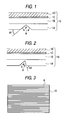
- Examples of the optical film are shown in Figs. 1 and 2.
- Figs. 1 and 2 are side views each showing a cross section of each of the light output portions (optical path changing slopes) in the optical film. In each of Figs.
- the optical film (transparent film) 10 includes light output portions A having optical path changing slopes a .
- the reference numeral 1C designates a bonding layer; and 1D, a release film.
- Figs. 1 and 2 show the case where a base material film 1B is used in the condition that a light output portions-forming layer 1A is attached to the base material film 1B, the invention may be applied also to the case where a single layer having the light output portions-forming layer is used alone without using any based material film.
- the optical film 10 is disposed in a direction along a panel plane of a liquid-crystal display panel having a light source 51 on a side surface of the panel so that the light-output-portions-A-forming surface of the optical film 10 faces outward.
- the optical film 10 is provided so that light incident on the side surface of the panel from the light source or transmitted light thereof is reflected by the optical path changing slopes a so that the optical path of the light is changed toward a rear surface of the transparent film 10 opposite to the light output portions-forming surface of the transparent film 10 and, accordingly, in a viewing direction of the liquid-crystal display panel.
- the reflected light finally exits from the transparent film so that the outgoing light can be used as illumination light (display light) of the liquid-crystal display panel.
- the transparent film can be made of one member or two or more members selected from the group of suitable materials exhibiting transparency to a wavelength region of light made incident on the transparent film from a light source.
- suitable materials exhibiting transparency to a wavelength region of light made incident on the transparent film from a light source.
- examples of the materials used in a visible light region include: transparent resins represented by acrylic-based resin, polycarbonate-based resin, cellulose-based resin and norbornene-based resin; and curable resins polymerizable by heat or by radial rays such as ultraviolet rays or electron rays.
- the preferred refractive index of the transparent film from the point of view to improve the efficiency of incidence of light onto the optical path changing slopes to thereby obtain a liquid-crystal display device with display excellent in brightness and uniformity of brightness is equal to or higher than that of the liquid-crystal display panel, particularly that of each of the panel substrates.
- the preferred refractive index is not lower than 1.49, particularly not lower than 1.52.
- the refractive index is not higher than 1.6, particularly not higher than 1.56, more particularly not higher than 1.54.
- the refractive index is generally based on a D line when light is in a visible light region.
- the refractive index need not be limited to the range as described above but may be set in accordance with the wavelength region of incident light when the wavelength region of incident light has specificity (this rule applies hereunder).
- the preferred transparent film from the point of view to suppress luminance unevenness and color unevenness to obtain a liquid-crystal display device little in display unevenness is a transparent film exhibiting no or little birefringence, particularly having an average in-plane retardation of 30 nm or smaller.
- a transparent film having such a small retardation is used, the state of polarization of incident light can be kept good to be favorable for prevention of the display quality from being deteriorated in the condition that the incident light is linearly polarized by a polarizer.
- the preferred average in-plane retardation in the transparent film from the point of view to prevent display unevenness is not larger than 20 nm, particularly not larger than 15 nm, more particularly not larger than 10 nm. It is further preferable that variation in the retardation in accordance with the place is as small as possible. From the point of view to suppress internal stress easily generated in the transparent film by a bonding process to thereby prevent the retardation from being generated by the internal stress, it is further preferable that the transparent film is made of a material having a small photoelastic coefficient.
- the average thicknesswise retardation of the transparent film is not larger than 50 nm, particularly not larger than 30 nm, more particularly not larger than 20 nm.
- Such a low-retardation transparent film can be formed by a suitable method such as a method of removing internal optical distortion of an existing film by annealing the existing film.
- the preferred method for forming such a low-retardation transparent film is a casting method.
- the retardation in the transparent film is based on light in a visible light region, particularly light with a wavelength of 550 nm.
- the transparent film is generally formed as a single layer film but may be formed as a laminate of one kind or different kinds of materials.
- the thickness of the transparent film can be determined suitably without any particular limitation. From the point of view of reduction in thickness and weight, it is preferable that the thickness of the transparent film is set to be in a range of from 5 to 500 ⁇ m, particularly in a range of from 10 to 300 ⁇ m, more particularly in a range of from 20 to 100 ⁇ m. When the thickness of the transparent film is set to be in this range, sizing can be performed easily by a punching process or the like.
- Light output portions A for obtaining this exit characteristic are provided on one of opposite surfaces of the transparent film to thereby form an optical film.
- the light output portions A are constituted by concave or convex portions having optical path changing slopes a each inclined at an inclination angle ⁇ 1 of from 35 to 48 degrees with respect to a film plane of the transparent film.
- each of the light output portions A has two optical path changing slopes a shaped like two sides of an isosceles triangle in section.
- Fig. 1 by way of example, each of the light output portions A has two optical path changing slopes a shaped like two sides of an isosceles triangle in section.
- each of the light output portions A has an optical path changing slope a inclined at an inclination angle ⁇ 1 of from 35 to 48 degrees with respect to the film plane, and a steep slope b inclined at a large inclination angle ⁇ 2 with respect to the film plane, the two slopes being shaped like two sides of an approximate triangle in section.
- the optical path of light incident on a side surface of a liquid-crystal display panel from a light source disposed on the side surface or the optical path of transmitted light of the incident light is changed toward the rear surface (opposite to the surface having the light output portions) of the transparent film by the optical path changing slopes a so that light excellent in directivity in a direction of a line normal to the liquid-crystal display panel can be made to exit from the transparent film with good efficiency of utilizing light emitted from the light source.
- the optical path of the light is changed by the optical path changing slopes each having an inclination angle lower than 35 degrees, and the light is then reflected by a reflection plate disposed on the back side (opposite to the visual side) of the liquid-crystal displaypanel, the angle of display light exiting from the panel on the basis of the reflected light exceeds 30 degrees to thereby result in a disadvantage in visibility.
- the inclination angle of each of the optical path changing slopes is higher than 48 degrees, total reflection cannot be performed and light leakage from the slopes occurs easily to thereby result in deterioration in light-utilizing efficiency.
- discrimination between the concave portions and the convex portions is based on whether the light output portions are depressed (as grooves) in the optical film or whether the light output portions are protruded (as peaks) from the optical film.
- the inclination angle ⁇ 1 of each of the optical path changing slopes is in a range of from 38 to 45 degrees, particularly in a range of from 40 to 43 degrees.
- the optical path changing slopes a are provided so that incident light from the light source in an illumination mode is reflected toward the rear surface of the transparent film to thereby change the optical path of the light.
- the light output portions having such optical path changing slopes are distributed over a surface of the transparent film so that the total luminous transmittance is in a range of from 75 to 92 % and the haze is in a range of from 4 to 20 %, there can be obtained a surface light source in which the optical path of light incident on a side surface from the light source is changed to illuminate the liquid-crystal display panel efficiently.
- the optical film has the total luminous transmittance in a range of from 80 to 91 % and the haze to be not larger than 15 %, particularly to be not larger than 12 %.
- the characteristic such as total luminous transmittance and haze can be achieved by controlling the size of each light output portion, or the distribution density of the light output portions. In this case, if the size is too large or if the density is too high, the probability that light transmitted inside the liquid-crystal display panel will become incident on the optical path changing slopes increases to be thereby favorable for illumination of the LCD, but, on the other hand, the probability that light reflected by a reflection plate on the rear surface will strike the light output portions when the reflected light used as illumination light is transmitted through the optical film again also increases. As a result, liquid-crystal display is disordered and contrast is lowered.
- the total luminous transmittance and haze in the invention are provided for determining the size and distribution density of the light output portions in order to achieve good display quality.
- the projected area occupied by the light output portions in the light output portions-forming surface of the transparent film is set to be in a range of from 1/100 to 1/8, particularly in a range of from 1/50 to 1/10, more particularly in a range of from 1/30 to 1/15, the total luminous transmittance and haze in the invention can be achieved.
- the light output portions may be constituted by concave or convex portions continuous from one side to the other side or may be constituted by concave or convex portions discontinuously intermittent.
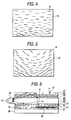
- the light output portions may be distributed in parallel with one another as shown in Fig. 3, may be distributed at random as shown in Fig. 4 or may be distributed in the form of pits arranged on concentric circles with a virtual center as their centers as shown in Fig. 5, on the basis of the optical path changing slopes in the condition that the light output portions are continuous or discontinuous.
- Each of the concave or convex portions constituting the light output portions may be formed into any suitable shape such as an approximate triangular shape, an approximate tetragonal shape or an approximate pentagonal shape in cross section with respect to the optical path changing slopes .
- the light output portions are generally constituted by concave or convex portions each shaped like an approximate triangle in section as shown in Figs. 1 and 2.
- the word "approximate" used in the approximate triangle or the like means that deformation such as changing of angles between sides, or rounding of angles formed between intersection points of sides is allowed.
- the achievement of the characteristic such as the total luminous transmittance and haze can be determined suitably in accordance with the shape of each light output portion, the method of distributing the light output portions, and so on.
- the repetition pitch thereof is set to be not larger than 2 mm, particularly in a range of from 20 ⁇ m to 1 mm, more particularly in a range of from 50 to 500 ⁇ m, while the projected width of each of the optical path changing slopes on the film plane is set to be not larger than 40 ⁇ m, particularly in a range of from 3 to 20 ⁇ m, more particularly in a range of from 5 to 15 ⁇ m.
- the parallel distribution of the continuous light output portions may be performed so that the light output portions are parallel with one side of the optical film or arranged to cross one side of the optical film at an angle of not higher than 30 degrees.
- the latter case is effective in preventing moire from being caused by interference of the light output portions with pixels of the liquid-crystal display panel.
- Prevention of moire can be also performed by adjustment of the repetition pitch of the parallel arrangement. Accordingly, the repetition pitch may vary and need not be constant.
- discontinuous light output portions are to be distributed in parallel with one another or at random as shown in Fig. 4 or to be distributed in the form of pits on concentric circles with a virtual center as their centers as shown in Fig. 5, it is preferable from the point of view to achieve the characteristic such as total luminous transmittance and haze that the light output portions are formed so that the length of each of the optical path changing slopes in a direction of the long side thereof is not smaller than 5 times, particularly not smaller than 8 times, more particularly not smaller than 10 times as large as the depth or height of each of the concave or convex portions.
- each of the optical path changing slopes is set to be not larger than 200 ⁇ m, particularly not larger than 170 ⁇ m, more particularly in a range of from 10 to 150 ⁇ m, while the depth or height of each of the concave or convex portions is set to be not smaller than 2 ⁇ m, particularly not larger than 20 ⁇ m, more particularly not larger than 10 ⁇ m.
- the width of each of the light output portions is set to be in a range of from 3 to 20 ⁇ m, particularly in a range of from 5 to 15 ⁇ m, and that the length of each of the light output portions is set to be not smaller than 5 times, particularly not smaller than 8 times as large as the width thereof.
- the length is based on the length of each of the optical path changing slopes in a direction of the long side thereof, that is, based on the continuous direction of grooves or peaks of the concave or convex portions, and the depth or height is based on the light output portions-forming surface of the transparent film.
- the width is based on a length in a direction perpendicular to the length, that is, based on a length in a direction of projection of the short side of each of the optical path changing slopes onto the film plane.
- the surfaces which form the light output portions but do not satisfy the optical path changing slopes a with a predetermined inclination angle, for example, the steep slopes b opposite to the optical path changing slopes a do not contribute to exiting of light incident on a side surface of the panel from the rear surface and do not have any influence on display quality and transmission/exiting of light as much as possible.
- the inclination angle ⁇ 2 of each of the steep slopes with respect to the film plane is too small, the projected area of the steep slopes on the film plane becomes large. As a result, surface-reflected light by the steep slopes is apt to return to an observing direction to thereby disturb display quality in an external light mode using front light arrangement.
- the inclination angle ⁇ 2 of each of the steep slopes increases.
- the projected area of the steep slopes on the film plane can be reduced, so that lowering of the total luminous transmittance and increase of the haze can be suppressed.
- the vertical angle between each of the optical path changing slopes and a corresponding one of the steep slopes can be also reduced, so that surface-reflected light can be reduced.
- the reflected light can be inclined in a direction of the plane (film plane) of the optical film, so that the influence on liquid-crystal display can be suppressed.
- the preferred inclination angle ⁇ 2 of each of the steep slopes is not smaller than 50 degrees, particularly not smaller than 60 degrees, more particularly in a range of from 75 to 90 degrees.
- Each of the slopes which form the light output portions A may be formed into a suitable surface shape such as a linear surface shape, a bent surface shape, or a curved surface shape.
- the sectional shape of the light output portions A may be formed so that the inclination angles of the light output portions take a constant value on the whole surface of a sheet.
- the light output portions may be formed so that the size of the light output portions A increases as the location thereof becomes farther from the side surface on which the light is incident, in order to cope with absorption loss and attenuation of transmitted light due to the changing of the optical path to thereby attain uniformity of light emission on the optical film.
- the light output portions A may be arranged at intervals of a constant pitch. Alternatively, as shown in Figs.
- the light output portions A may be arranged so that the pitch becomes narrow gradually to increase the distribution density of the light output portions A as the location of the light output portions A becomes farther from the side surface on which the light is incident. Further, the light output portions A may be arranged at intervals of a random pitch so that uniformity of light emission on the optical film can be attained. The random pitch is also advantageous from the point of view to prevent moire from being caused by interference of the light output portions with pixels. Accordingly, the light output portions A may be constituted by a combination of concave portions or convex portions different in shape or the like as well as different in pitch.
- each of the concave or convex portions is provided as a surface inclined at an angle of not lower than 30 degrees, particularly not lower than 45 degrees, more particularly not lower than 60 degrees.
- the concave shape of the light output portion is preferred to the convex shape.
- a point light source is disposed on a side surface of the liquid-crystal display panel.
- the optical path of light radiated from the point light source so as to be incident on the side surface or transmitted light thereof is changed by the optical path changing slopes a so that the rear surface of the optical film is made luminous as evenly as possible.
- light excellent in directivity in a direction normal to the liquid-crystal display panel is made to exit from the transparent film with good efficiency of utilizing light emitted from the light source.
- the pit-like arrangement of the light output portions A is preferably performed so that the point light source can be arranged easily and so that at least one virtual center can be formed on or outside an end surface of the transparent film.
- One virtual center may be formed or two or more virtual centers may be formed with respect to one film end surface or different film end surfaces.
- the transparent film having the light output portions can be formed by a suitable method.
- the method include: a method of transferring a shape to a thermoplastic resin by hot-pressing the thermoplastic resin against a mold capable of forming a predetermined shape; a method of filling a mold capable of forming a predetermined shape with a hot-melted thermoplastic resin or with a resin fluidized by heat or by a solvent; and a method of performing a polymerizing process after filling a mold capable of forming a predetermined shape with a liquid resin polymerizable by heat or by radial rays such as ultraviolet rays or electron rays or after casting the liquid resin in the mold.
- the method is particularly advantageous in the case where a transparent film and light output portions are integrally molded to form a body having structural layers of the transparent film and the light output portions.
- the preferred method of forming the transparent film having the light output portions is a method of adding the light output portions having optical path changing slopes onto a surface of the transparent film through a mold having a predetermined concave/convex structure.
- the preferred method include: a method in which a surface of a transparent film is coated with a curable resin polymerizable by ultraviolet rays, radial rays or the like, the coating layer is disposed close to the surface of the mold having the predetermined concave/convex structure therein and is cured by irradiation with ultraviolet rays, radial rays or the like and then the transparent film is separated from the mold and collected; and a method in which the surface of the mold having the predetermined concave/convex structure therein is filled with the curable resin, the transparent film is disposed closely onto the filler layer, the filler layer is cured by irradiation with ultraviolet rays, radial rays or the like and then the transparent film is separated from the mold and
- the efficiency in exiting of light may be reduced greatly because of interface reflection if the refractive index difference between the structural layer of the light output portions to be added and the transparent film is large.
- the refractive index difference between the transparent film and the structural layer of the light output portions is set to be as small as possible, particularly not larger than 0.10, more particularly not larger than 0.05.
- the refractive index of the structural layer of the light output portions to be added is set to be higher than that of the transparent film.
- a suitable transparent material selected in accordance with the wavelength region of incident light as listed as materials for the transparent film can be used for forming the structural layer of the light output portions.
- the front and rear surfaces of the optical film except the portion of the light output portions are flat surfaces as smooth as possible, particularly flat surfaces with an angular change in a range of ⁇ 2 degrees, more particularly flat surfaces with an angular change of zero degree.
- the angular change is preferably set to be not larger than 1 degree per 5 mm.
- the optical film may be formed so that a transparent bonding layer 1C is provided on the surface of the transparent film 1B opposite to the surface having the light output portions A as occasion demands.
- the bonding layer is provided for bonding the optical film to a support member such as a liquid-crystal display panel.
- the bonding process through the bonding layer is provided for improving the efficiency of reflection by the optical path changing slopes a of the light output portions A and, accordingly, for improving luminance on the basis of effective utilization of light incident on the side surface. It is preferable from these purposes that the refractive index difference between the transparent film and the bonding layer is small.
- the bonding layer has a refractive index which is not lower than a value lower by 0.07 than that of the transparent film and which is higher than or substantially equal to that of each of panel substrates of the liquid-crystal display panel.
- the refractive index of the bonding layer is lower than that of each of the panel substrates of the liquid-crystal display panel, light incident on the side surface is apt to be totally reflected when the incident light is transmitted.
- a resin plate or an optical glass plate is generally used as each of the panel substrates.
- the refractive index thereof is generally in a range of from about 1.51 to about 1.52.
- the non-alkali glass plate when the non-alkali glass plate is ideally subjected to a bonding process through a bonding layer having a refractive index of not lower than 1.52, a large part of the transmitted light with the angle allowed to be made incident onto the optical film from the panel can be made incident on the optical film without total reflection in the bonding interface between the panel and the bonding layer.
- the refractive index difference in each interface between transmission type optical layers such as the bonding layer, the liquid-crystal display panel, and the transparent film is set to be not larger than 0.15, particularly not larger than 0.10, more particularly not larger than 0.05.
- a suitable material satisfying this refractive index such as an adhesive agent curable by heat or by irradiation with ultraviolet rays, radial rays or the like, can be used for forming the bonding layer without any limitation.
- an adhesive layer can be used preferably.
- An adhesive agent containing a suitable polymer as a base polymer can be used for forming the adhesive layer.
- the base polymer examples include a rubber-based polymer, an acrylic-based polymer, a vinyl-alkyl ether-based polymer, a silicone-based polymer, a polyester-based polymer, a polyurethane-based polymer, a polyether-based polymer, a polyamide-based polymer, and a styrene-based polymer.
- an adhesive agent excellent in transparency, weather resistance and heat resistance can be used preferably.
- An example of the preferred adhesive agent is an acrylic-based adhesive agent in which a polymer mainly containing acrylic or metacrylic alkyl ester is used as a base polymer.
- the bonding layer may contain one member or two or more members selected from the group of suitable transparent particles so as to be provided as a light-diffusing bonding layer.
- suitable transparent particles include inorganic particles and organic particles.
- the inorganic particles are made of silica, alumina, titania, zirconia, tin oxide, indium oxide, cadmium oxide, antimony oxide, etc. and may be electrically conductive.
- the organic particles are made of a crosslinked or non-crosslinked polymer.
- a release sheet may be preferably temporarily bonded to the bonding layer so that the bonding layer is covered with the release sheet before the adhesive layer is put into practical use for the purpose of anti-contamination against foreign matters.
- the light output portions-forming surface of the optical film may be subjected to a non-glare treatment or an anti-reflection treatment in accordance with necessity for preventing viewing from being disturbed by surface reflection of external light.
- the light output portions-forming surface of the optical film may be subjected to a hard coat treatment for preventing the optical film from being injured.
- the optical film subjected to such a treatment can be preferably used particularly in a front light system.
- the surface By conducting a non-glare treatment on a surface, the surface can be formed as a fine concave/convex structure.
- Various methods may be used in the non-glare treatment.
- Examples of the methods include: a surface roughening method such as a sandblasting method and an embossing method; and a method of coating a surface with a resin containing transparent particles of silica or the like as listed above.
- the anti-reflection treatment can be made by a method of forming a coherent vapor-deposited film.
- the hard coat treatment can be made by a method of coating a surface with a hard resin such as curable resin.
- the non-glare treatment, the anti-reflection treatment or the hard coat treatment can be made by a method in which films subjected to one kind or two or more kinds of the treatments are bonded to one another.
- the optical film may at least have a linear polarizing element which is bonded and laminated onto the surface of the transparent film opposite to the surface with the light output portions so that the optical film is disposed on a liquid-crystal display panel.
- the optical film of the type having such a linear polarizing element bonded and laminated in advance is favorable for stability of quality, and improvement of efficiency in production of the liquid-crystal display device.
- the linear polarizing element it is possible to use a suitable one without any particular limitation. From the point of view of obtaining display with a good contrast ratio based on the incidence of highly linearly polarized light, a polarizing element with a high degree of polarization can be preferably used.
- the polarizing element is an absorption type polarizing film formed in such a manner that a dichromatic substance such as iodine or dichromatic dye is adsorbed into a hydrophilic polymeric film such as a polivinyl alcohol-based film, a partially formalized polivinyl alcohol-based film, or a partially saponified ethylene-vinyl acetate copolymer-based film, and then the film is oriented.
- a dichromatic substance such as iodine or dichromatic dye
- a hydrophilic polymeric film such as a polivinyl alcohol-based film, a partially formalized polivinyl alcohol-based film, or a partially saponified ethylene-vinyl acetate copolymer-based film
- a transparent protective layer in accordance with the related art may be provided on one or each of opposite surfaces of the linear polarizing element to be used.
- a material excellent in transparency, mechanical strength, heat stability, and moisture sealability, and having a reflective index as listed in the transparent film can be preferably used for forming the transparent protective layer.
- the optical film can be provided to serve also as a transparent protective layer for protecting the linear polarizing element. In this case, the size and weight of the liquid-crystal display device can be reduced more greatly.
- a transparent bonding layer for bonding the optical film to another member may be provided on the surface of the laminate opposite to the transparent film, that is, on the surface in which the linear polarizing element is provided, in accordance with necessity.
- the bonding layer can be formed in accordance with the case for the transparent film.
- the optical path of light incident on the side surface from the light source or transmitted light thereof is changed by the light exit portions (optical path changing slopes) in a direction (of a normal line) excellent in perpendicularity favorable for viewing so that the light can exit with good light-utilizing efficiency.
- the optical film can exhibit good transparency to external light.
- various kinds of devices such as a reflection type or transmission type liquid-crystal display device which is bright and easy to view both in an external light mode and in an illumination mode, and which is thin in thickness and light in weight.
- Fig. 6 shows an example of the liquid-crystal display device. The device shown in Fig.
- FIG. 6 is a reflection type liquid-crystal display device which can be used both in an external light mode and in an illumination mode.
- the reference numerals 20 and 30 designate panel substrates of a liquid-crystal display panel; 40, a liquid-crystal layer; and 31, a reflection layer.
- the liquid-crystal display device can be formed by arrangement of the optical film 10 on one surface of the liquid-crystal display panel so that the surface of the optical film 10 having the light output portions A faces outward.
- one light source 51 or two or more light sources 51 are arranged on one side surface or two or more side surfaces of the liquid-crystal display panel, particularly on one side surface or two or more side surfaces of the panel substrate 20 where the optical film 10 is disposed.
- an illuminating mechanism can be formed.
- a point light source is disposed on a side surface of the liquid-crystal display panel on a perpendicular line containing a virtual center of the light output portions A arranged in the form of pits, from the point of view to achieve bright display by efficiently using incident light radiated from the point light source.
- a suitable measure such as a measure of protruding the side of the panel substrate 20 on which the point light source will be disposed as shown in Fig. 6 can be taken in accordance with whether the virtual center of the light output portions A is disposed on or outside the end surface of the optical film.
- the light source disposed on the side surface of the liquid-crystal display panel it is possible to use a suitable one.
- the light source include: a point light source such as a light-emitting diode as described above; a linear light source such as a (cold or hot) cathode tube; an array in which such point light sources are set in a linear or planar array; and a combination of a point light source and a linear light guide plate through which incident light from the point light source is converted into a linear light source.
- the light source is disposed on a side surface of the panel so that the optical path changing slopes of the optical film face the light source.
- the optical path changing slopes are arranged, including the case of the pit-like arrangement, so that the optical path changing slopes face the light source as perpendicularly as possible, light incident on the side surface from the light source can be converted into light of a surface light source efficiently so that light can be emitted with high efficiency.
- two light sources may be disposed on opposite side surfaces of the panel substrate.
- one point light source or two or more point light sources may be disposed in accordance with one virtual center or two or more virtual centers of the light output portions in the optical film.
- the light source is provided so that viewing can be performed in an illumination mode in which the light source is switched on.
- the light source need not be switched on when viewing is performed in an external light mode using external light. Therefore, the light source is formed so as to be able to be switched on/off.
- the method for switching on/off the light source it is possible to use any method. Any one of related-art methods can be used.
- the light source may be of a different color emission type in which the color of emitted light can be changed. Further, different kinds of light sources maybe provided so that different color emission can be made through the different kinds of light sources.
- the light source 51 may be provided with a suitable auxiliary unit such as a reflector 52 for enclosing the light source 51 to lead diverging light onto a side surface of the liquid-crystal display panel as occasion demands. That is, the light source 51 is combined with the suitable auxiliary unit to form a combination body.
- a suitable reflection sheet such as a resin sheet coated with a high-reflectance metal thin film, a white sheet, or a sheet of metal foil.
- the reflector can be used as a fixing unit serving also as a unit for enclosing the light source by a method of bonding end portions of the reflector to end portions of the panel substrate.
- the liquid-crystal display device is formed by suitably assembling a liquid-crystal display panel functioning as a liquid-crystal shutter, a driver attached to the liquid-crystal display panel and a front light or backlight and by suitably assembling constituent parts such as a polarizer, a reflection layer or a compensating phase retarder as occasion demands.
- the invention is not particularly limited except that the optical film and the light source are used for forming an illuminating mechanism.
- the liquid-crystal display device can be formed in accordance with a related-art front light or backlight type device. Hence, the liquid-crystal displaypanel used is not particularly limited. As shown in Fig.
- liquid-crystal display panel examples include: a twisted or non-twisted liquid-crystal display panel such as a TN type liquid-crystal display panel, an STN type liquid-crystal display panel, an IPS type liquid-crystal display panel, an HAN type liquid-crystal display panel, an OCB type liquid-crystal display panel, and a VA type liquid-crystal display panel; a guest-host-based or ferroelectric liquid-crystal-based liquid-crystal display panel; and a light-diffusing liquid-crystal display panel such as an internal diffusion type liquid-crystal display panel.
- a suitable one such as an active matrix method or a passive matrix method may be used as Driving liquid crystal is generally performed through electrodes 21 and 31 provided on the inner sides of the panel substrates respectively as shown in Fig. 6.
- the arrangement of a reflection layer is essential to a reflection type liquid-crystal display device.
- the position of arrangement of the reflection layer is optional.
- the reflection layer may be provided inside the liquid-crystal display panel as shown in Fig. 6 or may be provided outside the liquid-crystal display panel.
- the electrode 31 serves also as a reflection layer.
- the reflection layer can be formed as a suitable reflection layer according to the related art.
- the reflection layer examples include: a coating layer containing powder of a high-reflectance metal such as aluminum, silver, gold, copper or chromium in a binder resin; a layer of a metal thin film deposited by a vapor deposition method; a reflection sheet having the coating or deposited layer supported by a base material; a sheet of metal foil; a transparent electrically conductive film; and a dielectric multilayer film.
- a coating layer containing powder of a high-reflectance metal such as aluminum, silver, gold, copper or chromium in a binder resin
- a layer of a metal thin film deposited by a vapor deposition method a reflection sheet having the coating or deposited layer supported by a base material
- a sheet of metal foil a transparent electrically conductive film
- a dielectric multilayer film When the liquid-crystal display device is provided as a transmission type one which can be used both in an external light mode and in an illumination mode, a suitable reflection film in the same manner as described above can be
- a transmission type liquid-crystal display device can be formed by arrangement of the optical film on the back side (opposite to the visual side) of the liquid-crystal display panel.
- the reflection layer is provided on the back side (outside) of the optical film, light leaked from the optical path changing slopes of the light output portions can be reflected by the reflection layer to return toward the liquid-crystal display panel.
- the leaked light can be utilized for illuminating the panel, so that improvement of luminance can be attained.
- the reflection layer is provided as a diffuse reflection surface, the reflected light can be diffused toward the frontal direction, that is, toward a direction more effective in viewing.
- the liquid-crystal display device can be used as transmission type one which can be used both in an external light mode and in an illumination mode.
- the panel substrates and electrodes of the panel need to be formed as transparent substrates and transparent electrodes to make liquid-crystal display possible.
- the electrode 31 serving also as a reflection layer is provided inside the liquid-crystal display panel as shown in Fig. 6, the visual side panel substrate 20 and electrode 21 need to be formed as a transparent substrate and a transparent electrode respectively to make liquid-crystal display possible.
- the back side panel substrate 30 need not be transparent as well as the reflection layer 31 need not be transparent. That is, the back side panel substrate 30 may be formed as an opaque body.
- each of the panel substrates is not particularly limited but may be determined suitably in accordance with the strength of enclosure of liquid crystal, the magnitude of the light source disposed, and so on. Generally, from the point of view of the balance between efficiency in light transmission and reduction in thickness and weight, it is preferable that the thickness is set to be in a range of from 10 ⁇ m to 5 mm, particularly in a range of from 50 ⁇ m to 2 mm, more particularly in a range of from 100 ⁇ m to 1 mm.
- the thickness of the panel substrate may vary so that a thickness difference is formed between the side where the light source is disposed and the side where the light source is not disposed.
- alignment films 22 and 32 such as rubbing films for aligning liquid crystal, a color filter 23 for achieving color display, a low-refractive-index layer 24, a linear polarizing element or polarizer 25, and a phase retarder 26, as shown in Fig. 6, may be provided as occasion demands.
- the alignment films are generally disposed so as to be adjacent to the liquid-crystal layer.
- the color filter is generally disposed between one of the panel substrates and a corresponding one of the electrodes.
- the polarizer is provided for controlling display light through linear polarization.
- the polarizer is disposed in a suitable position on one or each of the visual and back sides of the liquid-crystal display panel.
- the polarizer is used in accordance with necessity and in accordance with the display type based on the liquid crystal in the liquid-crystal display panel.
- the liquid-crystal display device can be formed as a device having nopolarizer.
- the polarizer it is possible to use a suitable one in accordance with the linear polarizing element. From the point of view of obtaining display with a good contrast ratio on the basis of incidence of highly linearly polarized light, a polarizer with a high degree of polarization can be used preferably.
- the low-refractive-index layer is provided so that light incident on the side surface from the light source is transmitted rearward in a direction of moving farther from the light source efficiently by interface reflection.
- the low-refractive-index layer can be formed as a transparent layer made of a suitable low-refractive-index material formed from inorganic or organic compounds such as a fluorine compound.
- the low-refractive-index layer is disposed on the inner side of the panel substrate 20 on which the light source 51 is disposed as shown in Fig. 6, that is, on the surface of the substrate opposite to the surface on which the optical film is provided.
- the refractive index of the low-refractive-index layer is lower by 0.01 or more, particularly by a value of from 0.02 to 0.15, more particularly by a value of from 0.05 to 0.10 than that of the panel substrate.
- the liquid-crystal display panel may be additionally provided with one suitable optical layer or two or more suitable optical layers such as a light-diffusing layer and a phase retarder, in accordance with necessity, as well as the non-glare layer.
- the light-diffusing layer is provided for the purposes of: enlargement of the display area by diffusing display light; uniformity of luminance by leveling light emission; increase in the quantity of light incident on the optical film by diffusing transmitted light inside the liquid-crystal display panel; and so on.
- the optical layer to be added may be integrally laminated on the optical film through an adhesive layer or the like in accordance with necessity so that the integrated body can be applied to the liquid-crystal display panel.
- the light-diffusing layer can be provided by a suitable method using a coating layer or a diffusing sheet having a surface fine concave/convex structure in accordance with the non-glare layer.
- the light-diffusing layer may be provided with an adhesive layer containing transparent particles so that the light-diffusing layer serves also as a bonding layer. In this case, reduction in thickness of the liquid-crystal display device can be attained.
- One light-diffusing layer or two or more light-diffusing layers may be disposed in one suitable positioner two or more suitable positions, for example, between the optical film and the visual side panel substrate.
- the phase retarder is provided for the purposes of: enlargement of the viewing angle by optical compensation; prevention of coloring; and so on. As shown in Fig. 6, the phase retarder is generally disposed between the visual side or back side polarizer and a corresponding one of the panel substrates. A suitable phase retarder in accordance with the wavelength region may be used as a compensating phase retarder.
- the phase retarder may be formed as one retardation layer or as a superposed layer of two or more retardation layers.
- the retarter plate may be formed as a suitable plate, such as: a birefringent film obtained in a manner so that a film formed from any suitable transparent polymer is oriented by a suitable method such as a uniaxal or biaxial orienting method; an alignment film of a suitable nematic or discotic liquid-crystal polymer; or a film in which such an alignment layer is supported by a transparent substrate.
- the phase retarder may have a thicknesswise refractive index controlled plate under the function of heat-shrinking force of a heat-shrinkable film.
- the transmission type liquid-crystal display device viewing both in an external light mode and in an illumination mode is performed as follows.
- an illumination mode in which the light source is switched on
- display light transmitted is viewed.
- an external light mode in which the light source is switched off, external light entering through the visual side surface and passing through the polarizer or the like is transmitted through the liquid-crystal display panel and reaches the optical film.
- light entering through other portions than the light output portions of the light output portions-forming surface of the optical film is inverted by the reflection layer provided on the back and transmitted inside the liquid-crystal display panel in the reverse course.
- display light is viewed.
- parts for forming the liquid-crystal display panel for forming the liquid-crystal display device may be wholly or partially integrally laminated and fixed to one another or may be disposed so as to be easily separable. From the point of view of suppressing interface reflection to prevent lowering of contrast, it is preferable that such parts are fixed to one another. It is preferable that at least the optical film and the liquid-crystal display panel are fixed and stuck to each other.
- a suitable transparent adhesive agent such as an adhesive agent can be used for the fixing process.
- Transparent particles may be contained in the transparent adhesive layer so that the transparent adhesive layer can be provided as an adhesive layer exhibiting a light-diffusing function.
- the parts for forming the liquid-crystal display panel may be made to have ultraviolet absorptive power, for example, by a method of treating them with an ultraviolet absorbent such as a salicylic ester-based compound, a benzophenone-based compound, a benzotriazole-based compound, a cyanoacrylate-based compound, or a nickel complex salt-based compound.
- an ultraviolet absorbent such as a salicylic ester-based compound, a benzophenone-based compound, a benzotriazole-based compound, a cyanoacrylate-based compound, or a nickel complex salt-based compound.
- a transparent film of polycarbonate (PC) 60 ⁇ m thick was coated with an ultraviolet-curable acrylic-based resin about 100 ⁇ m thick by use of an applicator.
- the coating layer of the acrylic-based resin was brought into close contact with a mold processed into a predetermined shape in advance by a rubber roller so that excessive resin and air bubbles were extruded out.
- the coating layer of the acrylic-based resin was cured by irradiation with ultraviolet rays from a metal halide lamp.
- the PC film coated with the acrylic resin was separated from the mold and cut into a predetermined size.
- the PC film was separated from the coating layer of the acrylic-based resin.
- the refractive index of the ultraviolet-curable resin measured after curing was 1.515.
- the optical film was 30 mm wide and 40 mm long.
- the optical film had light output portions constituted by concave portions which had optical path changing slopes and slopes opposite to the optical path changing slopes respectively.
- the optical path changing slopes were continuous in a direction of the width of the optical film and arranged in parallel with one another at intervals of a pitch of 210 ⁇ m in a direction of the length of the optical film.
- Each of the optical path changing slopes and a corresponding one of the slopes opposite to the optical path changing slopes formed two sides of a triangle in section.
- the projected width of each of the optical path changing slopes on a film plane of the optical film was 10 ⁇ m
- the inclination angle of each of the optical path changing slopes was 42.5 degrees
- the inclination angle of a corresponding one of the slopes opposite to the optical path changing slopes was about 75 degrees.
- the area of flat surfaces constituted by other portions than the light output portions in the surface in which the light output portions were formed was not smaller than 12 times as large as the sum of the area of the optical path changing slopes and the area of the slopes opposite to the optical path changing slopes.
- the measured total luminous transmittance and haze of the optical film were 89 % and 7 % respectively.
- An optical film was obtained in the same manner as in Example 1 except that a mold different in concave/convex shape was used in Example 2 .
- the optical film had light output portions each 100 ⁇ m long and 10 ⁇ m wide.
- Each of the light output portions was constituted by a combination of an optical path changing slope having an inclination angle of 42 degrees and an opposite slope having an inclination angle of 75 degrees.
- the combination of the two kinds of slopes formed two sides of a triangle in section.
- the light output portions were arranged in parallel with one another at intervals of a pitch of 210 ⁇ m in a direction of the length of the optical film in the condition that the light output portions were intermittent in a direction of the width of the optical film.
- the measured total luminous transmittance and haze of the optical film were 85 % and 10 % respectively.
- An optical film of the type having large-size light output portions disposed densely was obtained in the same manner as in Example 1 except that a mold different in concave/convex shape was used in Comparative Example 1.
- the optical film had optical path changing slopes disposed at intervals of a pitch of 130 ⁇ m.
- the projected width of each of the optical path changing slopes on the film plane was in a range of from 20 to 25 ⁇ m.
- Each of the optical path changing slopes satisfied a predetermined inclination angle.
- the total luminous transmittance and haze of the optical film were 70 % and 28 % respectively.
- An optical film of the type having small-size light output portions disposed roughly was obtained in the same manner as in Example 1 except that a mold different in concave/convex shape was used in Comparative Example 2.
- the optical film had optical path changing slopes disposed at intervals of a pitch of 500 ⁇ m.
- the projected width of each of the optical path changing slopes on the film plane was 5 ⁇ m.
- Each of the optical path changing slopes satisfied a predetermined inclination angle.
- the total luminous transmittance and haze of the optical film were 93 % and 3 % respectively.
- An optical film of the type having optical path changing slopes each not satisfying a predetermined inclination angle was obtained in the same manner as in Example 1 except that a mold different in concave/convex shape was used in Comparative Example 3.
- the projected width of each of the optical path changing slopes on the film plane was 10 ⁇ m.
- the maximum inclination angle of the optical path changing slopes was 15 degrees.
- the inclination angle of slopes opposite to the optical path changing slopes was 55 degrees.
- the pitch of the optical path changing slopes was 210 ⁇ m.
- the total luminous transmittance and haze of the optical film measured were 90 % and 6 % respectively.
- Magnesium fluoride was applied onto a polished non-alkali glass plate by vapor deposition to thereby form a low-refractive-index layer. Then, a plasma treatment was applied to the low-refractive-index layer in an argon atmosphere and an indium-tin oxide thin film was sputtered on the low-refractive-index layer to thereby form a transparent electrode. In this manner, a pair of transparent panel substrates were produced. As the visual side panel substrate on this occasion, substrates each having ten transparent electrodes 1 mm wide, 0.5 mm wide, 0.4 mm wide, 0.3 mm wide, 0.2 mm wide or 0.1 mm wide were formed.
- a polyvinyl alcohol film was formed on each of the transparent electrodes in the pair of substrates by spin coating. After the film was subjected to a rubbing treatment, the pair of substrates were disposed so that the transparent electrodes faced each other and so that the rubbing axes crossed each other perpendicularly. Then, a gap adjusting material made of spherical glass beads was disposed between the pair of substrates and the pair of substrates were fixed to each other by a sealing material. Then, a mixture solution containing 200 parts by weight of liquid crystal (E-7, made by BDH COMPANY) and 1 part by weight of a chiral agent (MC-32, made by MERCK & CO., INC.) was injected between the pair of substrates. Thus, a liquid-crystal cell was obtained.
- E-7 liquid crystal
- MC-32 chiral agent
- a polarizer was stuck onto the outer side of the visual side transparent substrate in the liquid-crystal cell obtained as described above so that the rubbing axis was made coincident with the absorption axis .
- Apolarizer having a reflection layer was stuck onto the outer side of the back side substrate so that the absorption axis of the back side polarizer crossed that of the visual side polarizer perpendicularly and so that the reflection layer was disposed outward.
- An acrylic-based adhesive agent with a refractive index of 1.515 was used as an agent for bonding each of the polarizers.
- a cold-cathode tube as an illumination light source was disposed on a side surface of the visual side substrate in the reflection type TN liquid-crystal display panel.
- the cold-cathode tube was covered with a reflection film having a film surface made of a silver thin film. Opposite ends of the reflection film were stuck to upper and lower end portions of the liquid-crystal display panel so that light was prevented from being leaked.
- the optical film obtained in each of Examples 1 and 2 and Comparative Examples 1 to 3 was stuck to the visual side of the reflection type TN liquid-crystal display panel by use of an adhesive agent with a refractive index of 1.515 so that the light output portions-forming surface of the optical film faced outward and so that the direction of the length of the optical path changing slopes was parallel with the end surface on which the cold-cathode tube was disposed.
- a reflection type liquid-crystal display device was produced and disposed on a black board.
- Example 1 Example 2 Compa-rative Example 1 Compa-rative Example 2 Compa-rative Example 3 Frontal Luminance (cd/m 2 ) 24 22 16 4 4
- Examples 1 and 2 were superior in brightness to Comparative Examples 1 to 3. In terms of external appearance in light emission, brightness in each of Examples 1 and 2 was more uniform than that in each of Comparative Examples 1 to 3.
- Comparative Example 1 when light reflected by the back side reflection layer passed through the optical film again, the haze was so large that the light could not exit toward the observer. Hence, in Comparative Example 1, display was dark because the light could not substantially contribute to illumination for the liquid-crystal display device.
- the total luminous transmittance of the film was high and the haze thereof was small so that the optical path of light from the light source could not be changed sufficiently. Hence, in Comparative Example 2, display was very dark.
- Comparative Example 3 the direction of outgoing light was inclined largely so that the light could not contribute to illumination for the panel. Hence, in Comparative Example 3, display was dark.
- the light source can be provided on a side surface of the liquid-crystal display panel to illuminate the panel without necessity of using any separately provided light guide plate to thereby make it possible to form a transmission type or reflection type liquid-crystal display device which is thin, lightweight and capable of being used both in an external light mode and in an illumination mode.
Landscapes
- Physics & Mathematics (AREA)
- General Physics & Mathematics (AREA)
- Optics & Photonics (AREA)
- Nonlinear Science (AREA)
- Mathematical Physics (AREA)
- Chemical & Material Sciences (AREA)
- Crystallography & Structural Chemistry (AREA)
- Liquid Crystal (AREA)
- Optical Elements Other Than Lenses (AREA)
- Planar Illumination Modules (AREA)
- Polarising Elements (AREA)
Applications Claiming Priority (2)
| Application Number | Priority Date | Filing Date | Title |
|---|---|---|---|
| JP2001073243 | 2001-03-15 | ||
| JP2001073243A JP4986198B2 (ja) | 2001-03-15 | 2001-03-15 | 光学フィルム及び液晶表示装置 |
Publications (1)
| Publication Number | Publication Date |
|---|---|
| EP1241402A1 true EP1241402A1 (fr) | 2002-09-18 |
Family
ID=18930697
Family Applications (1)
| Application Number | Title | Priority Date | Filing Date |
|---|---|---|---|
| EP02006002A Withdrawn EP1241402A1 (fr) | 2001-03-15 | 2002-03-15 | Couche mince et affichage à cristaux liquides |
Country Status (5)
| Country | Link |
|---|---|
| US (1) | US7871680B2 (fr) |
| EP (1) | EP1241402A1 (fr) |
| JP (1) | JP4986198B2 (fr) |
| KR (1) | KR100802743B1 (fr) |
| TW (1) | TWI312428B (fr) |
Cited By (3)
| Publication number | Priority date | Publication date | Assignee | Title |
|---|---|---|---|---|
| WO2005124399A1 (fr) * | 2004-06-18 | 2005-12-29 | Toray Industries, Inc. | Film de diffusion anisotrope |
| US9188732B2 (en) | 2012-12-14 | 2015-11-17 | Lg Display Co., Ltd. | Display device and method for fabricating reflective sheet for the same |
| EP2905532A3 (fr) * | 2014-02-07 | 2015-12-09 | Himax Display, Inc. | Module d'affichage et dispositif de guidage de lumière |
Families Citing this family (22)
| Publication number | Priority date | Publication date | Assignee | Title |
|---|---|---|---|---|
| CN101829429B (zh) * | 2004-12-03 | 2011-12-07 | 世嘉股份有限公司 | 游戏装置 |
| US20060158437A1 (en) * | 2005-01-20 | 2006-07-20 | Blythe Michael M | Display device |
| US8603288B2 (en) | 2008-01-18 | 2013-12-10 | Rockwell Collins, Inc. | Planarization treatment of pressure sensitive adhesive for rigid-to-rigid substrate lamination |
| US8936057B2 (en) * | 2005-08-30 | 2015-01-20 | Rockwell Collins, Inc. | Substrate lamination system and method |
| US8137498B2 (en) | 2005-08-30 | 2012-03-20 | Rockwell Collins Inc. | System and method for completing lamination of rigid-to-rigid substrates by the controlled application of pressure |
| US9939526B2 (en) | 2007-09-06 | 2018-04-10 | Rockwell Collins, Inc. | Display system and method using weather radar sensing |
| US9733349B1 (en) | 2007-09-06 | 2017-08-15 | Rockwell Collins, Inc. | System for and method of radar data processing for low visibility landing applications |
| KR101763710B1 (ko) | 2008-01-18 | 2017-08-01 | 로크웰 콜린스 인코포레이티드 | 기판 적층 시스템 및 방법 |
| JP5221193B2 (ja) * | 2008-04-17 | 2013-06-26 | 住友電気工業株式会社 | 配光制御パネルおよび移動体搭載用表示装置 |
| KR20100135295A (ko) * | 2008-04-17 | 2010-12-24 | 스미토모덴키고교가부시키가이샤 | 배광 제어 패널, 이동체 탑재용 표시 장치, 배광 제어 시트, 광학 부품, 조명 장치 및 표시 장치 |
| KR101252092B1 (ko) * | 2009-04-01 | 2013-04-12 | 엘지디스플레이 주식회사 | 백라이트 유닛과 이를 이용한 액정표시장치 |
| US8486535B1 (en) | 2010-05-24 | 2013-07-16 | Rockwell Collins, Inc. | Systems and methods for adherable and removable thin flexible glass |
| US8647727B1 (en) * | 2012-06-29 | 2014-02-11 | Rockwell Colllins, Inc. | Optical assembly with adhesive layers configured for diffusion |
| US9262932B1 (en) | 2013-04-05 | 2016-02-16 | Rockwell Collins, Inc. | Extended runway centerline systems and methods |
| US9981460B1 (en) | 2014-05-06 | 2018-05-29 | Rockwell Collins, Inc. | Systems and methods for substrate lamination |
| US10928510B1 (en) | 2014-09-10 | 2021-02-23 | Rockwell Collins, Inc. | System for and method of image processing for low visibility landing applications |
| US10705201B1 (en) | 2015-08-31 | 2020-07-07 | Rockwell Collins, Inc. | Radar beam sharpening system and method |
| US10228460B1 (en) | 2016-05-26 | 2019-03-12 | Rockwell Collins, Inc. | Weather radar enabled low visibility operation system and method |
| US10353068B1 (en) | 2016-07-28 | 2019-07-16 | Rockwell Collins, Inc. | Weather radar enabled offshore operation system and method |
| US11119330B2 (en) * | 2017-06-02 | 2021-09-14 | Nikon Corporation | Reticle, reticle unit, rifle scope, and optical apparatus |
| TWI800176B (zh) * | 2021-12-23 | 2023-04-21 | 元太科技工業股份有限公司 | 前光模組與電泳顯示器 |
| CN116339033A (zh) * | 2021-12-23 | 2023-06-27 | 川奇光电科技(扬州)有限公司 | 前光模块与电泳显示器 |
Citations (11)
| Publication number | Priority date | Publication date | Assignee | Title |
|---|---|---|---|---|
| JPH05158033A (ja) * | 1991-12-03 | 1993-06-25 | Sharp Corp | 液晶表示装置 |
| US6027220A (en) * | 1996-11-19 | 2000-02-22 | Enplas Corporation | Surface light source device outputting polarized frontal illumination light |
| JP2000147449A (ja) * | 1998-11-09 | 2000-05-26 | Matsushita Electric Ind Co Ltd | 液晶プロジェクションテレビ |
| EP1111440A2 (fr) * | 1999-12-20 | 2001-06-27 | Nitto Denko Corporation | Dispositif d'affichage à cristal liquide |
| EP1113310A2 (fr) * | 1999-12-27 | 2001-07-04 | Nitto Denko Corporation | Dispositif à cristal liquide opérant en mode dual en réflexion et transmission |
| US20010010630A1 (en) * | 2000-01-13 | 2001-08-02 | Seiji Umemoto | Light pipe and method for producing the same |
| EP1122586A2 (fr) * | 2000-02-02 | 2001-08-08 | Nitto Denko Corporation | Film optique |
| US20010012159A1 (en) * | 2000-02-02 | 2001-08-09 | Seiji Umemoto | Optical film |
| EP1126312A2 (fr) * | 2000-02-14 | 2001-08-22 | Nitto Denko Corporation | Réflecteur et dispositif d'affichage à cristaux liquides |
| US20010020984A1 (en) * | 1999-12-06 | 2001-09-13 | Seiji Umemoto | Light pipe, plane light source unit and liquid-crystal display device |
| EP1154306A1 (fr) * | 2000-05-12 | 2001-11-14 | Nitto Denko Corporation | Dispositif d'affichage à cristaux liquides du type réflectif |
Family Cites Families (25)
| Publication number | Priority date | Publication date | Assignee | Title |
|---|---|---|---|---|
| JPS5570816A (en) * | 1978-11-22 | 1980-05-28 | Seiko Epson Corp | Production of liquid crystal panel |
| US4374612A (en) * | 1980-07-25 | 1983-02-22 | Canon Kabushiki Kaisha | Mark indicating device for optical apparatus |
| EP0201323B1 (fr) * | 1985-05-07 | 1994-08-17 | Dai Nippon Insatsu Kabushiki Kaisha | Article comprenant un hologramme transparent |
| US5485354A (en) | 1993-09-09 | 1996-01-16 | Precision Lamp, Inc. | Flat panel display lighting system |
| US6159608A (en) * | 1995-09-28 | 2000-12-12 | Saint-Gobain Performance Plastics Corporation | Thermoplastic interlayer film |
| JP3373106B2 (ja) * | 1996-03-27 | 2003-02-04 | 株式会社きもと | 光学フィルム |
| JP3644787B2 (ja) * | 1996-05-09 | 2005-05-11 | 松下電器産業株式会社 | 面状照明系 |
| JPH103813A (ja) * | 1996-06-14 | 1998-01-06 | Sharp Corp | バックライト装置 |
| US6097514A (en) * | 1996-07-31 | 2000-08-01 | Dai Nippon Printing Co., Ltd. | Hologram replicating method, and volume hologram |
| JPH10123329A (ja) * | 1996-10-16 | 1998-05-15 | Seiko Epson Corp | 照明装置および液晶表示装置 |
| JPH10260640A (ja) * | 1997-03-19 | 1998-09-29 | Sanyo Electric Co Ltd | バックライト装置 |
| JP3518237B2 (ja) * | 1997-03-28 | 2004-04-12 | カシオ計算機株式会社 | 液晶表示装置 |
| EP0879991A3 (fr) * | 1997-05-13 | 1999-04-21 | Matsushita Electric Industrial Co., Ltd. | Système d'illumination |
| TW505685B (en) * | 1997-09-05 | 2002-10-11 | Mitsubishi Materials Corp | Transparent conductive film and composition for forming same |
| JPH11184388A (ja) * | 1997-12-19 | 1999-07-09 | Stanley Electric Co Ltd | 反射型液晶表示装置 |
| JP3680903B2 (ja) * | 1998-02-13 | 2005-08-10 | オムロン株式会社 | 面光源装置 |
| JPH11260132A (ja) * | 1998-03-12 | 1999-09-24 | Omron Corp | 面光源装置 |
| JPH11271768A (ja) * | 1998-03-23 | 1999-10-08 | Sekisui Chem Co Ltd | 導光板及び面状光源装置 |
| JPH11297115A (ja) * | 1998-04-14 | 1999-10-29 | Nitto Denko Corp | 導光板、面光源装置及び反射型液晶表示装置 |
| JPH11352479A (ja) * | 1998-06-12 | 1999-12-24 | Dainippon Printing Co Ltd | バックライト装置及び透過型表示装置 |
| JP2000056138A (ja) * | 1998-08-11 | 2000-02-25 | Taiho Ind Co Ltd | 導光板及び面発光体 |
| JP3410977B2 (ja) * | 1998-09-14 | 2003-05-26 | シャープ株式会社 | フロントライト及び反射型液晶表示装置 |
| JP3394460B2 (ja) * | 1998-11-09 | 2003-04-07 | 株式会社日立製作所 | 反射型液晶表示装置 |
| JP2000251515A (ja) * | 1998-12-28 | 2000-09-14 | Seiko Epson Corp | 面状発光体、反射型表示装置及び電子機器 |
| JP2001028202A (ja) * | 1999-07-14 | 2001-01-30 | Citizen Electronics Co Ltd | フロントライト光源 |
-
2001
- 2001-03-15 JP JP2001073243A patent/JP4986198B2/ja not_active Expired - Fee Related
-
2002
- 2002-03-14 KR KR1020020013736A patent/KR100802743B1/ko not_active Expired - Fee Related
- 2002-03-14 US US10/096,935 patent/US7871680B2/en not_active Expired - Fee Related
- 2002-03-15 EP EP02006002A patent/EP1241402A1/fr not_active Withdrawn
- 2002-03-15 TW TW091104944A patent/TWI312428B/zh not_active IP Right Cessation
Patent Citations (11)
| Publication number | Priority date | Publication date | Assignee | Title |
|---|---|---|---|---|
| JPH05158033A (ja) * | 1991-12-03 | 1993-06-25 | Sharp Corp | 液晶表示装置 |
| US6027220A (en) * | 1996-11-19 | 2000-02-22 | Enplas Corporation | Surface light source device outputting polarized frontal illumination light |
| JP2000147449A (ja) * | 1998-11-09 | 2000-05-26 | Matsushita Electric Ind Co Ltd | 液晶プロジェクションテレビ |
| US20010020984A1 (en) * | 1999-12-06 | 2001-09-13 | Seiji Umemoto | Light pipe, plane light source unit and liquid-crystal display device |
| EP1111440A2 (fr) * | 1999-12-20 | 2001-06-27 | Nitto Denko Corporation | Dispositif d'affichage à cristal liquide |
| EP1113310A2 (fr) * | 1999-12-27 | 2001-07-04 | Nitto Denko Corporation | Dispositif à cristal liquide opérant en mode dual en réflexion et transmission |
| US20010010630A1 (en) * | 2000-01-13 | 2001-08-02 | Seiji Umemoto | Light pipe and method for producing the same |
| EP1122586A2 (fr) * | 2000-02-02 | 2001-08-08 | Nitto Denko Corporation | Film optique |
| US20010012159A1 (en) * | 2000-02-02 | 2001-08-09 | Seiji Umemoto | Optical film |
| EP1126312A2 (fr) * | 2000-02-14 | 2001-08-22 | Nitto Denko Corporation | Réflecteur et dispositif d'affichage à cristaux liquides |
| EP1154306A1 (fr) * | 2000-05-12 | 2001-11-14 | Nitto Denko Corporation | Dispositif d'affichage à cristaux liquides du type réflectif |
Non-Patent Citations (1)
| Title |
|---|
| PATENT ABSTRACTS OF JAPAN vol. 2000, no. 08 6 October 2000 (2000-10-06) * |
Cited By (5)
| Publication number | Priority date | Publication date | Assignee | Title |
|---|---|---|---|---|
| WO2005124399A1 (fr) * | 2004-06-18 | 2005-12-29 | Toray Industries, Inc. | Film de diffusion anisotrope |
| CN100430756C (zh) * | 2004-06-18 | 2008-11-05 | 东丽株式会社 | 各向异性扩散薄膜 |
| US9188732B2 (en) | 2012-12-14 | 2015-11-17 | Lg Display Co., Ltd. | Display device and method for fabricating reflective sheet for the same |
| EP2905532A3 (fr) * | 2014-02-07 | 2015-12-09 | Himax Display, Inc. | Module d'affichage et dispositif de guidage de lumière |
| US9341883B2 (en) | 2014-02-07 | 2016-05-17 | Himax Display, Inc. | Display module and light guide device |
Also Published As
| Publication number | Publication date |
|---|---|
| KR100802743B1 (ko) | 2008-02-12 |
| JP2002277615A (ja) | 2002-09-25 |
| KR20020073404A (ko) | 2002-09-26 |
| US7871680B2 (en) | 2011-01-18 |
| JP4986198B2 (ja) | 2012-07-25 |
| US20020187284A1 (en) | 2002-12-12 |
| TWI312428B (en) | 2009-07-21 |
Similar Documents
| Publication | Publication Date | Title |
|---|---|---|
| US7871680B2 (en) | Optical film and liquid-crystal display device | |
| US7227685B2 (en) | Optical film and liquid-crystal display device | |
| EP1209510B1 (fr) | Film optique et dispositif d'affichage à cristaux liquides du type réflectif | |
| JP4442836B2 (ja) | 光学フィルム | |
| US6950155B2 (en) | Liquid-crystal display device | |
| US6603520B2 (en) | Optical film and liquid-crystal display device | |
| EP1199512A1 (fr) | Substrat en verre et dispositif d'affichage à cristaux liquides | |
| US20030210367A1 (en) | Reflection-type liquid-crystal display, and optical film | |
| US6888595B2 (en) | Reflector and liquid-crystal display device | |
| US6882474B2 (en) | Optical path changing polarizer | |
| US6768529B2 (en) | Reflection-transmission double type liquid-crystal display device | |
| JP2012022336A (ja) | 光学フィルム及び液晶表示装置 | |
| JP2003131227A (ja) | 液晶表示装置 | |
| JP4462517B2 (ja) | 光学フィルム及び液晶表示装置 | |
| JP4462514B2 (ja) | 光学フィルムおよび液晶表示装置 | |
| JP2002341344A (ja) | 透過型液晶表示装置 | |
| JP2004184790A (ja) | 光学フィルム及び液晶表示装置 |
Legal Events
| Date | Code | Title | Description |
|---|---|---|---|
| PUAI | Public reference made under article 153(3) epc to a published international application that has entered the european phase |
Free format text: ORIGINAL CODE: 0009012 |
|
| AK | Designated contracting states |
Kind code of ref document: A1 Designated state(s): AT BE CH CY DE DK ES FI FR GB GR IE IT LI LU MC NL PT SE TR |
|
| AX | Request for extension of the european patent |
Free format text: AL;LT;LV;MK;RO;SI |
|
| 17P | Request for examination filed |
Effective date: 20030129 |
|
| AKX | Designation fees paid |
Designated state(s): NL |
|
| REG | Reference to a national code |
Ref country code: DE Ref legal event code: 8566 |
|
| STAA | Information on the status of an ep patent application or granted ep patent |
Free format text: STATUS: THE APPLICATION IS DEEMED TO BE WITHDRAWN |
|
| 18D | Application deemed to be withdrawn |
Effective date: 20090925 |