EP1248128B1 - Optischer Stecker, Halterungsvorrichtung für optisches Element und Montageteil für einen optischen Stecker - Google Patents
Optischer Stecker, Halterungsvorrichtung für optisches Element und Montageteil für einen optischen Stecker Download PDFInfo
- Publication number
- EP1248128B1 EP1248128B1 EP02007167A EP02007167A EP1248128B1 EP 1248128 B1 EP1248128 B1 EP 1248128B1 EP 02007167 A EP02007167 A EP 02007167A EP 02007167 A EP02007167 A EP 02007167A EP 1248128 B1 EP1248128 B1 EP 1248128B1
- Authority
- EP
- European Patent Office
- Prior art keywords
- main body
- housing
- section
- body section
- optical
- Prior art date
- Legal status (The legal status is an assumption and is not a legal conclusion. Google has not performed a legal analysis and makes no representation as to the accuracy of the status listed.)
- Expired - Lifetime
Links
- 230000003287 optical effect Effects 0.000 title claims description 69
- 239000007769 metal material Substances 0.000 claims description 7
- 239000011347 resin Substances 0.000 claims description 6
- 229920005989 resin Polymers 0.000 claims description 6
- 230000005693 optoelectronics Effects 0.000 claims 4
- 238000003780 insertion Methods 0.000 description 12
- 230000037431 insertion Effects 0.000 description 12
- 230000000717 retained effect Effects 0.000 description 5
- 238000004891 communication Methods 0.000 description 4
- 229910052751 metal Inorganic materials 0.000 description 4
- 239000002184 metal Substances 0.000 description 4
- 230000000694 effects Effects 0.000 description 3
- 230000005855 radiation Effects 0.000 description 2
- 229910000838 Al alloy Inorganic materials 0.000 description 1
- 229910052782 aluminium Inorganic materials 0.000 description 1
- XAGFODPZIPBFFR-UHFFFAOYSA-N aluminium Chemical compound [Al] XAGFODPZIPBFFR-UHFFFAOYSA-N 0.000 description 1
- 239000004020 conductor Substances 0.000 description 1
- 238000010276 construction Methods 0.000 description 1
- 238000005516 engineering process Methods 0.000 description 1
- 238000010438 heat treatment Methods 0.000 description 1
- 238000009413 insulation Methods 0.000 description 1
- 238000000034 method Methods 0.000 description 1
Images


Classifications
-
- G—PHYSICS
- G02—OPTICS
- G02B—OPTICAL ELEMENTS, SYSTEMS OR APPARATUS
- G02B6/00—Light guides; Structural details of arrangements comprising light guides and other optical elements, e.g. couplings
- G02B6/24—Coupling light guides
- G02B6/42—Coupling light guides with opto-electronic elements
- G02B6/4201—Packages, e.g. shape, construction, internal or external details
- G02B6/4274—Electrical aspects
- G02B6/4277—Protection against electromagnetic interference [EMI], e.g. shielding means
-
- G—PHYSICS
- G02—OPTICS
- G02B—OPTICAL ELEMENTS, SYSTEMS OR APPARATUS
- G02B6/00—Light guides; Structural details of arrangements comprising light guides and other optical elements, e.g. couplings
- G02B6/24—Coupling light guides
- G02B6/42—Coupling light guides with opto-electronic elements
- G02B6/4201—Packages, e.g. shape, construction, internal or external details
- G02B6/4219—Mechanical fixtures for holding or positioning the elements relative to each other in the couplings; Alignment methods for the elements, e.g. measuring or observing methods especially used therefor
- G02B6/4236—Fixing or mounting methods of the aligned elements
- G02B6/4245—Mounting of the opto-electronic elements
-
- G—PHYSICS
- G02—OPTICS
- G02B—OPTICAL ELEMENTS, SYSTEMS OR APPARATUS
- G02B6/00—Light guides; Structural details of arrangements comprising light guides and other optical elements, e.g. couplings
- G02B6/24—Coupling light guides
- G02B6/42—Coupling light guides with opto-electronic elements
- G02B6/4201—Packages, e.g. shape, construction, internal or external details
- G02B6/4266—Thermal aspects, temperature control or temperature monitoring
- G02B6/4268—Cooling
- G02B6/4269—Cooling with heat sinks or radiation fins
-
- G—PHYSICS
- G02—OPTICS
- G02B—OPTICAL ELEMENTS, SYSTEMS OR APPARATUS
- G02B6/00—Light guides; Structural details of arrangements comprising light guides and other optical elements, e.g. couplings
- G02B6/24—Coupling light guides
- G02B6/42—Coupling light guides with opto-electronic elements
- G02B6/4292—Coupling light guides with opto-electronic elements the light guide being disconnectable from the opto-electronic element, e.g. mutually self aligning arrangements
-
- G—PHYSICS
- G02—OPTICS
- G02B—OPTICAL ELEMENTS, SYSTEMS OR APPARATUS
- G02B6/00—Light guides; Structural details of arrangements comprising light guides and other optical elements, e.g. couplings
- G02B6/24—Coupling light guides
- G02B6/42—Coupling light guides with opto-electronic elements
- G02B6/4201—Packages, e.g. shape, construction, internal or external details
- G02B6/4256—Details of housings
- G02B6/426—Details of housings mounting, engaging or coupling of the package to a board, a frame or a panel
Definitions
- the present invention relates to an optical connector, an optical element holding structure, and a structure of a mount section of an optical connector to be employed in the field of optical communication such as that used in office automation, factory automation, and vehicle-mounted equipment.
- optical connector which is to be fixedly mounted on a mount board while incorporating optical elements has been improved in terms of a noise resistance characteristic of optical elements for withstanding external noise.
- the optical elements are built into a connector housing while being housed in a shielding shell made of highly conductive material, such as metal.
- US 5,259,053 shows an optical connector formed of a main section and an end panel section, within which active optical devices are seated. The optical devices are urged into alignment when the end section is inserted in the main section.
- EP 0 524 406 A1 discloses an optical module in which a photoelectric transfer element is shielded on five sides by a metal cage having above to let out the light, and is soldered with its terminals to a plate or circuit board on the sixth side.
- US 4 737 008 and EP 0 320 214 show an optical connector similar to connector of US 5 259 053 where the electro-optical devices are urged into a housing recess of the connector housing by an end panel section.
- Figs. 4 and 5 show conceivable constructions for grounding a shielding shell of an optical connector of this type.
- a lead. terminal 106 is provided at right angles on a shielding shell 102 for sheathing an optical element D, so as to project downward beyond a connector housing 105. While the optical connector 101 is mounted on a mount board 108, the lead terminal 106 penetrates through the mount board 108 and is soldered to a trace for grounding purpose formed on a lower surface of the mount board 108 . As a result, the shielding shell 102 is grounded by way of the lead terminal 106.
- ground tab pieces 113 are formed on both sides of a shielding shell 112 so as to jut outward from both sides of a main body section of a connector housing 115.
- the optical connector 110 is fixedly mounted on a mount board 118 such that the tab pieces 113 are brought, in an overlappedmanner, into plane contact with ground traces 119 formed on an upper surface of the mount board 118.
- the shielding shell 112 is grounded by way of the tab pieces 113.
- the shielding shell 102 is merely grounded by way of the pin-shaped lead terminal 106. Hence, high ground resistance arises, and an insufficient electromagnetic shielding effect is achieved.
- an optical element is fittingly inserted into a housing recess formed in a metal case; an opening of the housing recess is formed so as to become slightly larger than the element main body so that the element main body of the optical element can be fitted into the recess.
- the tab pieces 113 are brought into plane contact with the ground traces 119. Hence, low ground resistance arises, and a sufficient electromagnetic shielding effect is achieved.
- the ground tab pieces 113 significantly jut outward from both sides of the main body section of the connector housing 115. Hence, there arises a problem of a necessity for using a large area for fixedly mounting the connector 101.
- the present invention has been conceived in light of the problem and is aimed at providing an optical connector and an optical element holding structure which are superior in countermeasures against heat as well as against noise.
- Another aim of the present invention is to provide a structure to be used for mounting an optical connector and provision of an optical connector, which enable minimizing of ground resistance of a shielding shell and minimizing of an area required for mounting an optical connector.
- the first aspect of this invention is an optical connector according to claim 1.
- a non-joint plane opposite to a joint plane of the closure section to be connected to the housing main body section may be housed in the connector housing in an outwardly exposed state, and a corrugated heatsinking fin section may be provided in the non-joint plane.
- the optical element may be embodied as a plurality of optical elements, and housing recesses into which the optical elements are to be housed may be formed in the case main body section independently and side by side while being partitioned from each other.
- the housing main body section and the closure section may be formed from metal material or conductive resin.
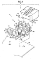
- an optical connector 1 is primarily constituted of, e.g., resin having an insulation characteristic; a shielding case 3 made of metal material having conductivity, such as aluminum or an aluminum alloy; and a light-emitting element 4 and a light-receiving element 5, which act as optical elements and are paired with each other.
- the shielding case 3 is formed in the shape of a substantially-rectangular parallelepiped.
- the shielding case 3 has a two-way split structure consisting of a case main body section 8 and a heatsink mechanism section 9.
- Housing recesses 7-into which are formed a rectangularly-parallelepiped element main body section 4a of the light-emitting element 4 and a rectangularly-parallelepiped element main body section 5a of the light-receiving element 5 are formed side by side in the case main body section 8 with reference to a widthwise direction thereof while being partitioned independently from each other.
- the heatsink mechanism section 9 acts as a closure section to be attached to the case main body section 8 from its back in order to close rear opening sections of the respective housing recesses 7 in the case main body section 8.
- a flat mount piece section 8a is projectingly formed in a lower end section on either side surface of the case main body section 8.
- a screw insertion hole 8b is formed in each mount piece section 8a.
- a front surface of the heat sink mechanism section 9 namely, a joint plane 9a to be connected to the rear surface of the case main body section 8, is formed into the shape of a flat plane.
- Trench sections 10 are formed in a rear surface of the heatsink mechanism section 9; that is, a non-joint plane 9b opposite to the joint plane 9a, so as to become spaced apart from each other at appropriate intervals in a widthwise direction and extend vertically, thus constituting a corrugated heatsink fin 11.
- Aplate-like mount piece section 9c is projectingly formed at a lower position on either side surface of the heatsink mechanism section 9.
- the mount piece sections 9c are superimposed on respective upper surfaces of the mount piece sections 8a.
- a screw insertion hole 9d to be brought into communication with the corresponding screw insertion hole 8b is formed in each of the mount piece sections 9c.
- each housing recess 7 is set so as to become slightly smaller than the cross directional thickness "t" of each of the element main body sections 4a, 5a such that the element main body sections 4a, 5a are retained in the corresponding housing recesses 7 in a sandwiched manner while the joint plane 9a of the heatsink mechanism section 9 is fitted into the back of the case main body section 8.
- a case housing recess 13 opens rearward in the back of the connector housing 2.
- the case main body section 8 of the shielding case 3 is fitted into the case housing recess 13.
- mount piece sections 2a are projectingly formed at lower positions on respective rear side surfaces of the connector housing 2, wherein the mount piece sections 2a are to be superimposed on respective upper surfaces of the mount pieces 9a of the heatsink mechanism section 9.
- Female thread holes 2b are formed in the respective mount piece sections 2a so as to be brought into communication with the respective screw insertion holes 8b and the screw insertion holes 9d.
- Cylindrical ferrule guide sections 14 are formed in the connector housing 2 so as to be brought into communication with the respective window sections 7a while the case main body section 8 of the shield case 2 is fitted into the case housing recess 13.
- the embodiment has been constructed in the foregoing manner.
- the element main body sections 4a, 5a of the optical elements 4, 5 are fittingly housed in the respective housing recesses 7 of the case main body section 8.
- the joint plane 9a of the heatsink mechanism section 9 is joined to the back of the case main body section 8 and while the case main body section 8 is fitted into the case housing recess 13 of the connector housing 2, the lead terminals 4b, 5b are inserted into insertion holes formed in a predetermined circuit pattern of the circuit board 16.
- a lower surface of the shield case 3 is placed at a predetermined location while remaining in plane contact with a ground circuit of the circuit board 16.
- each housing recess 7 is slightly smaller than the cross directional thickness "t" of each of the element main body sections 4a, 5a of the optical elements 4, 5.
- the element main body sections 4a, 5a of the optical elements 4, 5 are fittingly housed and held in a sandwiched manner in the respective housing recesses 7 formed in the shielding case 3 made of metal material; that is, a combination of the case main body section 8 and the heatsink mechanism section 9.
- the element main body sections 4a, 5a, the case main body section 8, and the heatsink mechanism section 9 can be retained tightly without involvement of clearance, thereby enabling efficient heat transfer and heatsinking.
- the case main body section 8 and the heatsink mechanism section 9 are held in plane contact with the ground circuit, thus realizing a superior shielding effect. There is yielded an advantage of superior countermeasures against noise and heat.
- the optical connector 1 can use the light-emitting element 4 and the light-receiving element 5, which operate at faster speed.
- the heatsink fin section 11 of the shield case 3 is housed and retained in the connector housing 2 in an outwardly-exposed manner.
- the heatsink fin section 11 enables more efficient radiation. Even in this regard, the optical connector is superior in measures against heat.
- the respective housing recesses 7 can hold the element main body sections 4a, 5a in stable positions and shield the same independently. Further, there can be ensured a wider contact area between the exterior surfaces of the element main body sections 4a, 5a and the interior surfaces of the respective housing recesses 7. Even in this regard, there is yielded an advantage of the ability to achieve superior countermeasures against noise and heat.
- the connector housing 2, the shielding case 3, and the optical elements 4, 5 can be fixedly mounted in one piece on the circuit board 16.
- the connector housing 2 is superior even in ease of assembly.
- the case main body section 8 and the heatsink mechanism 9 are respectively made of metal material.
- the case main body section 8 and the heatsink mechanism section 9 may be made of conductive resin.
- the optical elements 4, 5 can be retained in the respective housing recesses 7 in a sandwiched manner by means of elastic action of plastic and superior holding force.
- either the case main body section 8 or the heatsink mechanism section 9 may be formed from conductive resin.
- optical elements 4, 5 are of two-polarity type.
- the optical elements may be constructed in the same manner even when the optical elements are of single-polarity type or have three or more polarities.
- the connector housing 2, the case main body section 8, and the heatsink mechanism section 9 are fastened to the circuit board 16 with fastening screws. As a result, they are mounted and fixed on the circuit board 16 in one piece.
- the case main body section 8 and the heatsink mechanism section 9 maybe fastenedtogetherbeforehand, after which the thus-fixed shielding case 3 is housed in the case housing recess 13 of the connector housing 2.
- the connector housing 2 may be mounted on the circuit board 16.
- case main body section 8 is shown as having the housing recesses 7.
- the heatsink mechanism section 9 may have the housing recesses 7.
- recesses may be formed in the heatsink mechanism section 9 as well as in the case main body section 8 such that the housing recesses 7 are formed when they are joined together.
- a shielding case is formed in a split manner from a case main body section and a closure section, which constitute a housing recess when joined together.
- a case main body section and a closure section which constitute a housing recess when joined together.
- an element main body section of an optical element is situated in the housing recess and retained and sandwiched between the case main body section and the closure section.
- the optical element can be held tightly without involvement of clearance.
- a non-joint plane opposite to a joint plane of the closure section to be connected to the case main body section is to be housed in the connector housing in an outwardly exposed state.
- Acorrugated heatsinking f in section is provided in the non-joint plane.
- main body section and the closure section are formed from metal material, there is yielded an advantage of superior heatsinking. In contrast, when they are made of conductive resin, there is yielded an advantage of the ability to generate superior clamping force.
Landscapes
- Physics & Mathematics (AREA)
- General Physics & Mathematics (AREA)
- Optics & Photonics (AREA)
- Electromagnetism (AREA)
- Optical Couplings Of Light Guides (AREA)
Claims (5)
- Ein optischer Verbinder (1) zum Verbinden eines optischen Wellenleiters mit einem optoelektronischen Element, der Folgendes aufweist:ein Verbindergehäuse (2), das eine erste Gehäuseaussparung (13) aufweist, die sich zu einer Seite des Verbindergehäuses öffnet;einen Hauptkörperabschnitt (8) des Gehäuses, der passend in der ersten Gehäuseaussparung (13) untergebracht ist und eine zweite Gehäuseaussparung (7) umfasst, die sich zur selben Seite des Verbindergehäuses wie die erste Gehäuseaussparung öffnet;einen Schließabschnitt (9), der an dem Hauptkörperabschnitt (8) des Gehäuses angebracht ist, um die zweite Gehäuseaussparung (7) und die erste Gehäuseaussparung zu schließen;einen Elementhauptkörperabschnitt (4a, 5a) eines optoelektronischen Elements (4, 5), der passend in der zweiten Gehäuseaussparung (7) untergebracht ist, wobeider Hauptkörperabschnitt des Elements zwischen dem Hauptkörperabschnitt des Gehäuses und dem Schließabschnitt gehalten ist, wobei der Hauptkörperabschnitt (8) des Gehäuses und der Schließabschnitt (9) eine leitende Abschirmhülle (3) bilden, die mit einer Erdschaltung verbunden ist.
- Der optische Verbinder (1) nach Anspruch 1, wobei
der Schließabschnitt (9) eine verbundene Ebene (9a) umfasst, die mit dem Hauptkörperabschnitt des Gehäuses verbunden ist, und eine nicht verbundene Ebene (9b), die der verbundenen Ebene gegenüberliegt; und
wobei eine gerippte Wärmeableitungsfinne in der nicht verbundenen Ebene des Schließabschnitts (9) gebildet ist. - Der optische Verbinder (1) nach Anspruch 1, wobei der Schließabschnitt (9) aus Metallmaterial hergestellt ist.
- Der optische Verbinder (1) nach Anspruch 1, wobei
der Hauptkörperabschnitt (8) des Gehäuses und der Schließabschnitt (9) aus Metallmaterial oder leitendem Kunststoff hergestellt sind. - Der optische Verbinder (1) nach Anspruch 1, wobei das optoelektronische Element (4, 5) eine Vielzahl von optoelektronischen Elementen (4, 5) umfasst;
die zweite Gehäuseaussparung (7) eine Vielzahl von Gehäuseaussparungen (7) umfasst, in welchen die optoelektronischen Elemente (4, 5) untergebracht sind;
und wobei die Gehäuseaussparungen (7) in dem Hauptkörperabschnitt (8) des Gehäuses voneinander getrennt sind.
Priority Applications (1)
| Application Number | Priority Date | Filing Date | Title |
|---|---|---|---|
| EP05001350A EP1524538B1 (de) | 2001-04-03 | 2002-03-28 | Optischer Stecker, Halterungsvorrichtung für optisches Element und Montageteil für einen optischen Stecker |
Applications Claiming Priority (8)
| Application Number | Priority Date | Filing Date | Title |
|---|---|---|---|
| JP2001104426A JP2002303762A (ja) | 2001-04-03 | 2001-04-03 | 光コネクタ |
| JP2001104367A JP2002303764A (ja) | 2001-04-03 | 2001-04-03 | 光コネクタ |
| JP2001104367 | 2001-04-03 | ||
| JP2001104426 | 2001-04-03 | ||
| JP2001105479A JP2002299652A (ja) | 2001-04-04 | 2001-04-04 | シールドケースの光素子保持構造 |
| JP2001105479 | 2001-04-04 | ||
| JP2001176540 | 2001-06-12 | ||
| JP2001176540A JP2002365486A (ja) | 2001-06-12 | 2001-06-12 | 光コネクタの実装取付部の構造及び光コネクタ |
Related Child Applications (1)
| Application Number | Title | Priority Date | Filing Date |
|---|---|---|---|
| EP05001350A Division EP1524538B1 (de) | 2001-04-03 | 2002-03-28 | Optischer Stecker, Halterungsvorrichtung für optisches Element und Montageteil für einen optischen Stecker |
Publications (3)
| Publication Number | Publication Date |
|---|---|
| EP1248128A2 EP1248128A2 (de) | 2002-10-09 |
| EP1248128A3 EP1248128A3 (de) | 2004-06-02 |
| EP1248128B1 true EP1248128B1 (de) | 2007-08-15 |
Family
ID=27482171
Family Applications (2)
| Application Number | Title | Priority Date | Filing Date |
|---|---|---|---|
| EP02007167A Expired - Lifetime EP1248128B1 (de) | 2001-04-03 | 2002-03-28 | Optischer Stecker, Halterungsvorrichtung für optisches Element und Montageteil für einen optischen Stecker |
| EP05001350A Expired - Lifetime EP1524538B1 (de) | 2001-04-03 | 2002-03-28 | Optischer Stecker, Halterungsvorrichtung für optisches Element und Montageteil für einen optischen Stecker |
Family Applications After (1)
| Application Number | Title | Priority Date | Filing Date |
|---|---|---|---|
| EP05001350A Expired - Lifetime EP1524538B1 (de) | 2001-04-03 | 2002-03-28 | Optischer Stecker, Halterungsvorrichtung für optisches Element und Montageteil für einen optischen Stecker |
Country Status (3)
| Country | Link |
|---|---|
| US (3) | US6939054B2 (de) |
| EP (2) | EP1248128B1 (de) |
| DE (2) | DE60222815T2 (de) |
Families Citing this family (15)
| Publication number | Priority date | Publication date | Assignee | Title |
|---|---|---|---|---|
| JP4411506B2 (ja) * | 2002-09-18 | 2010-02-10 | 住友電気工業株式会社 | 光通信器 |
| JP2005116400A (ja) * | 2003-10-09 | 2005-04-28 | Auto Network Gijutsu Kenkyusho:Kk | 光アクティブコネクタ |
| DE102004009967B4 (de) * | 2004-03-01 | 2010-03-18 | Airbus Deutschland Gmbh | Kabelhalter für ein Flugzeug, Kabelhalterkit und Flugzeug mit einem Kabelhalter |
| JP4210240B2 (ja) * | 2004-06-03 | 2009-01-14 | ローム株式会社 | 光通信モジュール |
| CN201130260Y (zh) * | 2007-11-09 | 2008-10-08 | 富士康(昆山)电脑接插件有限公司 | 光纤连接器 |
| TWI475519B (zh) * | 2008-03-26 | 2015-03-01 | Nohmi Bosai Ltd | Photoelectric smoke detector |
| EP2138881A1 (de) * | 2008-06-24 | 2009-12-30 | Comoss Electronic Co. Ltd. | Optische Isoliervorrichtung und Glasfasersteckverbinder |
| WO2010146652A1 (ja) * | 2009-06-15 | 2010-12-23 | 富士通オプティカルコンポーネンツ株式会社 | 光モジュール |
| JP5222233B2 (ja) | 2009-06-16 | 2013-06-26 | 株式会社オートネットワーク技術研究所 | 光通信モジュール |
| US9389373B2 (en) * | 2012-09-24 | 2016-07-12 | The Boeing Company | Optical connector |
| JP5942967B2 (ja) * | 2013-11-29 | 2016-06-29 | 株式会社デンソー | 駆動装置 |
| JP7359579B2 (ja) * | 2019-07-05 | 2023-10-11 | 日東電工株式会社 | 光電気複合伝送モジュール |
| DE102020123465B4 (de) * | 2020-09-09 | 2022-03-17 | HARTING Electronics GmbH | Optoelektronisches Modul, optoelektronischer Steckverbinder und optoelektronische Unterverteilung |
| CN117276979A (zh) * | 2023-01-19 | 2023-12-22 | 东莞立讯技术有限公司 | 连接器组合件 |
| USD1119817S1 (en) | 2023-02-03 | 2026-03-24 | Dongguan Luxshare Technologies Co., Ltd | Cage of connector |
Family Cites Families (28)
| Publication number | Priority date | Publication date | Assignee | Title |
|---|---|---|---|---|
| US4539476A (en) * | 1980-11-28 | 1985-09-03 | Tokyo Shibaura Denki Kabushiki Kaisha | Module for a fiber optic link |
| US4477134A (en) * | 1981-08-14 | 1984-10-16 | Hewlett-Packard Company | Electrostatic discharge protected integrated circuit module |
| US4737008A (en) * | 1984-10-01 | 1988-04-12 | Mitsumi Electric Co., Ltd. | Optical transmitting and/or receiving module |
| US4840451A (en) * | 1987-12-08 | 1989-06-20 | Molex Incorporated | Shielded fiber optic connector assembly |
| JPH01169416A (ja) * | 1987-12-25 | 1989-07-04 | Hitachi Ltd | 光伝送モジュール |
| JP2858769B2 (ja) * | 1989-01-13 | 1999-02-17 | 日本エー・エム・ピー株式会社 | コネクタ |
| US5231685A (en) * | 1989-11-28 | 1993-07-27 | Kel Corporation | Multi-way electro-optic connector assemblies and optical fiber ferrule assemblies therefor |
| JPH03216607A (ja) * | 1990-01-22 | 1991-09-24 | Mitsubishi Rayon Co Ltd | 光電変換モジュールの製造法 |
| US5005939A (en) * | 1990-03-26 | 1991-04-09 | International Business Machines Corporation | Optoelectronic assembly |
| JPH04120759A (ja) * | 1990-09-12 | 1992-04-21 | Mitsubishi Rayon Co Ltd | シールドケース |
| US5137959A (en) * | 1991-05-24 | 1992-08-11 | W. R. Grace & Co.-Conn. | Thermally conductive elastomer containing alumina platelets |
| JP2544978Y2 (ja) * | 1991-06-06 | 1997-08-20 | 住友電気工業株式会社 | 光モジュール |
| JPH053330A (ja) * | 1991-06-25 | 1993-01-08 | Hitachi Ltd | 光送受信モジユール |
| US5259053A (en) * | 1992-06-29 | 1993-11-02 | The Whitaker Corporation | Discrete optical receptacle assembly with alignment feature |
| JPH0792342A (ja) * | 1993-07-29 | 1995-04-07 | Sumitomo Electric Ind Ltd | 光導波路モジュール |
| CA2133230C (en) * | 1993-09-30 | 2004-06-29 | Hiromi Kurashima | Optical module, method of manufacturing the same, and sleeve |
| JPH07207160A (ja) * | 1994-01-11 | 1995-08-08 | Toshiba Silicone Co Ltd | シリコーン組成物およびその製造方法 |
| US5671307A (en) * | 1995-04-10 | 1997-09-23 | Universite Laval | Use of a temperature gradient to impose a chirp on a fibre bragg grating |
| JP3111864B2 (ja) * | 1995-08-30 | 2000-11-27 | 住友電装株式会社 | 光ファイバコネクタ |
| US6333967B1 (en) * | 1996-07-19 | 2001-12-25 | Rigaku Corporation | X-ray generator |
| DE19637743A1 (de) * | 1996-09-16 | 1998-03-19 | Taiwan Liton Electronic Co | Abdichtungsverfahren und -vorrichtung zum Aussperren von elektromagnetischen Störungen durch Verkleben eines Metallgehäuses |
| US5763900A (en) * | 1996-12-05 | 1998-06-09 | Taiwan Liton Electronic Co. Ltd. | Infrared transceiver package |
| JP4015722B2 (ja) * | 1997-06-20 | 2007-11-28 | 東レ・ダウコーニング株式会社 | 熱伝導性ポリマー組成物 |
| GB2345799A (en) * | 1997-08-19 | 2000-07-19 | Taiyo Yuden Kk | Filler material for a wire wound electronic component |
| US6096414A (en) * | 1997-11-25 | 2000-08-01 | Parker-Hannifin Corporation | High dielectric strength thermal interface material |
| JP2958694B2 (ja) * | 1998-01-28 | 1999-10-06 | ローム株式会社 | 半導体光学装置のシールドケース |
| JP3444199B2 (ja) * | 1998-06-17 | 2003-09-08 | 信越化学工業株式会社 | 熱伝導性シリコーンゴム組成物及びその製造方法 |
| US6195267B1 (en) * | 1999-06-23 | 2001-02-27 | Ericsson Inc. | Gel structure for combined EMI shielding and thermal control of microelectronic assemblies |
-
2002
- 2002-03-28 EP EP02007167A patent/EP1248128B1/de not_active Expired - Lifetime
- 2002-03-28 DE DE60222815T patent/DE60222815T2/de not_active Expired - Lifetime
- 2002-03-28 DE DE60221736T patent/DE60221736T2/de not_active Expired - Lifetime
- 2002-03-28 EP EP05001350A patent/EP1524538B1/de not_active Expired - Lifetime
- 2002-04-01 US US10/109,684 patent/US6939054B2/en not_active Expired - Fee Related
-
2003
- 2003-10-09 US US10/681,299 patent/US6860643B2/en not_active Expired - Fee Related
- 2003-10-09 US US10/681,301 patent/US20040071412A1/en not_active Abandoned
Non-Patent Citations (1)
| Title |
|---|
| None * |
Also Published As
| Publication number | Publication date |
|---|---|
| DE60222815T2 (de) | 2008-07-03 |
| EP1248128A2 (de) | 2002-10-09 |
| EP1524538B1 (de) | 2007-10-03 |
| US6939054B2 (en) | 2005-09-06 |
| US20040071406A1 (en) | 2004-04-15 |
| DE60221736D1 (de) | 2007-09-27 |
| DE60222815D1 (de) | 2007-11-15 |
| DE60221736T2 (de) | 2008-06-05 |
| EP1248128A3 (de) | 2004-06-02 |
| EP1524538A1 (de) | 2005-04-20 |
| US20040071412A1 (en) | 2004-04-15 |
| US6860643B2 (en) | 2005-03-01 |
| US20020141706A1 (en) | 2002-10-03 |
Similar Documents
| Publication | Publication Date | Title |
|---|---|---|
| CN110690616B (zh) | 用于电连接器的热沉组件 | |
| US10993352B2 (en) | Thermal transfer device for a pluggable module assembly | |
| US6558191B2 (en) | Stacked transceiver receptacle assembly | |
| US6969280B2 (en) | Electrical connector with double mating interfaces for electronic components | |
| US5580283A (en) | Electrical connector having terminal modules | |
| EP3123572B1 (de) | Thermisch effizientes verbindersystem | |
| US8599567B2 (en) | Electronic module with improved printed circuit board to maximize width thereof | |
| US7972172B2 (en) | Cable end connector assembly | |
| US8814605B2 (en) | Power connector | |
| WO2008098050A2 (en) | Modular laser package system | |
| US6272021B1 (en) | Circuit device | |
| EP2492588B1 (de) | Festkörperbeleuchtungsanordnung mit Zugentlastungselement | |
| CN111478094A (zh) | 具有散热器的四通道小型可插拔双密度收发模块 | |
| EP1524538B1 (de) | Optischer Stecker, Halterungsvorrichtung für optisches Element und Montageteil für einen optischen Stecker | |
| US11646513B2 (en) | Electrical connector for high-frequency signal transmission | |
| US10361499B2 (en) | Signal transferring device and adapter assembly | |
| US10187988B1 (en) | Adapter with an insulating body having a circuit board with a plurality of conductive modules surface mounted on the board | |
| EP1248129B1 (de) | Optischer Stecker | |
| US6726374B2 (en) | GBIC with enhanced grounding | |
| US6565268B2 (en) | Optical connector and structure of optical connector-packaging/mounting portion | |
| US5261828A (en) | Misalignment tolerant edge connector assembly | |
| US8632361B2 (en) | Electrical connector | |
| US20240136741A1 (en) | Electrical Connector | |
| JP3937895B2 (ja) | 光モジュール | |
| JP2002303766A (ja) | 光コネクタ |
Legal Events
| Date | Code | Title | Description |
|---|---|---|---|
| PUAI | Public reference made under article 153(3) epc to a published international application that has entered the european phase |
Free format text: ORIGINAL CODE: 0009012 |
|
| AK | Designated contracting states |
Kind code of ref document: A2 Designated state(s): AT BE CH CY DE DK ES FI FR GB GR IE IT LI LU MC NL PT SE TR |
|
| AX | Request for extension of the european patent |
Free format text: AL;LT;LV;MK;RO;SI |
|
| RIC1 | Information provided on ipc code assigned before grant |
Ipc: 7H 01R 13/658 B Ipc: 7G 02B 6/42 A |
|
| PUAL | Search report despatched |
Free format text: ORIGINAL CODE: 0009013 |
|
| RIC1 | Information provided on ipc code assigned before grant |
Ipc: 7H 05K 9/00 B Ipc: 7H 01R 13/658 B Ipc: 7H 01L 23/60 B Ipc: 7G 02B 6/42 A Ipc: 7H 01L 31/0203 B |
|
| AK | Designated contracting states |
Kind code of ref document: A3 Designated state(s): AT BE CH CY DE DK ES FI FR GB GR IE IT LI LU MC NL PT SE TR |
|
| AX | Request for extension of the european patent |
Extension state: AL LT LV MK RO SI |
|
| 17P | Request for examination filed |
Effective date: 20040825 |
|
| 17Q | First examination report despatched |
Effective date: 20040916 |
|
| AKX | Designation fees paid |
Designated state(s): DE FR |
|
| GRAP | Despatch of communication of intention to grant a patent |
Free format text: ORIGINAL CODE: EPIDOSNIGR1 |
|
| GRAS | Grant fee paid |
Free format text: ORIGINAL CODE: EPIDOSNIGR3 |
|
| GRAA | (expected) grant |
Free format text: ORIGINAL CODE: 0009210 |
|
| AK | Designated contracting states |
Kind code of ref document: B1 Designated state(s): DE FR |
|
| REF | Corresponds to: |
Ref document number: 60221736 Country of ref document: DE Date of ref document: 20070927 Kind code of ref document: P |
|
| EN | Fr: translation not filed | ||
| PLBE | No opposition filed within time limit |
Free format text: ORIGINAL CODE: 0009261 |
|
| STAA | Information on the status of an ep patent application or granted ep patent |
Free format text: STATUS: NO OPPOSITION FILED WITHIN TIME LIMIT |
|
| 26N | No opposition filed |
Effective date: 20080516 |
|
| PGFP | Annual fee paid to national office [announced via postgrant information from national office to epo] |
Ref country code: DE Payment date: 20120411 Year of fee payment: 11 |
|
| PG25 | Lapsed in a contracting state [announced via postgrant information from national office to epo] |
Ref country code: FR Free format text: LAPSE BECAUSE OF FAILURE TO SUBMIT A TRANSLATION OF THE DESCRIPTION OR TO PAY THE FEE WITHIN THE PRESCRIBED TIME-LIMIT Effective date: 20080411 |
|
| REG | Reference to a national code |
Ref country code: DE Ref legal event code: R119 Ref document number: 60221736 Country of ref document: DE Effective date: 20131001 |
|
| PG25 | Lapsed in a contracting state [announced via postgrant information from national office to epo] |
Ref country code: DE Free format text: LAPSE BECAUSE OF NON-PAYMENT OF DUE FEES Effective date: 20131001 |