EP1248261A2 - Random und schnelles DRAM Speicher Direktzugriffmanagementsverfahren - Google Patents
Random und schnelles DRAM Speicher Direktzugriffmanagementsverfahren Download PDFInfo
- Publication number
- EP1248261A2 EP1248261A2 EP02354028A EP02354028A EP1248261A2 EP 1248261 A2 EP1248261 A2 EP 1248261A2 EP 02354028 A EP02354028 A EP 02354028A EP 02354028 A EP02354028 A EP 02354028A EP 1248261 A2 EP1248261 A2 EP 1248261A2
- Authority
- EP
- European Patent Office
- Prior art keywords
- block
- request
- memory
- requests
- address
- Prior art date
- Legal status (The legal status is an assumption and is not a legal conclusion. Google has not performed a legal analysis and makes no representation as to the accuracy of the status listed.)
- Withdrawn
Links
Images



Classifications
-
- G—PHYSICS
- G11—INFORMATION STORAGE
- G11C—STATIC STORES
- G11C11/00—Digital stores characterised by the use of particular electric or magnetic storage elements; Storage elements therefor
- G11C11/21—Digital stores characterised by the use of particular electric or magnetic storage elements; Storage elements therefor using electric elements
- G11C11/34—Digital stores characterised by the use of particular electric or magnetic storage elements; Storage elements therefor using electric elements using semiconductor devices
- G11C11/40—Digital stores characterised by the use of particular electric or magnetic storage elements; Storage elements therefor using electric elements using semiconductor devices using transistors
- G11C11/401—Digital stores characterised by the use of particular electric or magnetic storage elements; Storage elements therefor using electric elements using semiconductor devices using transistors forming cells needing refreshing or charge regeneration, i.e. dynamic cells
- G11C11/406—Management or control of the refreshing or charge-regeneration cycles
- G11C11/40618—Refresh operations over multiple banks or interleaving
-
- G—PHYSICS
- G11—INFORMATION STORAGE
- G11C—STATIC STORES
- G11C11/00—Digital stores characterised by the use of particular electric or magnetic storage elements; Storage elements therefor
- G11C11/21—Digital stores characterised by the use of particular electric or magnetic storage elements; Storage elements therefor using electric elements
- G11C11/34—Digital stores characterised by the use of particular electric or magnetic storage elements; Storage elements therefor using electric elements using semiconductor devices
- G11C11/40—Digital stores characterised by the use of particular electric or magnetic storage elements; Storage elements therefor using electric elements using semiconductor devices using transistors
- G11C11/401—Digital stores characterised by the use of particular electric or magnetic storage elements; Storage elements therefor using electric elements using semiconductor devices using transistors forming cells needing refreshing or charge regeneration, i.e. dynamic cells
- G11C11/406—Management or control of the refreshing or charge-regeneration cycles
-
- G—PHYSICS
- G11—INFORMATION STORAGE
- G11C—STATIC STORES
- G11C11/00—Digital stores characterised by the use of particular electric or magnetic storage elements; Storage elements therefor
- G11C11/21—Digital stores characterised by the use of particular electric or magnetic storage elements; Storage elements therefor using electric elements
- G11C11/34—Digital stores characterised by the use of particular electric or magnetic storage elements; Storage elements therefor using electric elements using semiconductor devices
- G11C11/40—Digital stores characterised by the use of particular electric or magnetic storage elements; Storage elements therefor using electric elements using semiconductor devices using transistors
- G11C11/401—Digital stores characterised by the use of particular electric or magnetic storage elements; Storage elements therefor using electric elements using semiconductor devices using transistors forming cells needing refreshing or charge regeneration, i.e. dynamic cells
- G11C11/4063—Auxiliary circuits, e.g. for addressing, decoding, driving, writing, sensing or timing
- G11C11/407—Auxiliary circuits, e.g. for addressing, decoding, driving, writing, sensing or timing for memory cells of the field-effect type
- G11C11/4076—Timing circuits
-
- G—PHYSICS
- G11—INFORMATION STORAGE
- G11C—STATIC STORES
- G11C11/00—Digital stores characterised by the use of particular electric or magnetic storage elements; Storage elements therefor
- G11C11/21—Digital stores characterised by the use of particular electric or magnetic storage elements; Storage elements therefor using electric elements
- G11C11/34—Digital stores characterised by the use of particular electric or magnetic storage elements; Storage elements therefor using electric elements using semiconductor devices
- G11C11/40—Digital stores characterised by the use of particular electric or magnetic storage elements; Storage elements therefor using electric elements using semiconductor devices using transistors
- G11C11/401—Digital stores characterised by the use of particular electric or magnetic storage elements; Storage elements therefor using electric elements using semiconductor devices using transistors forming cells needing refreshing or charge regeneration, i.e. dynamic cells
- G11C11/4063—Auxiliary circuits, e.g. for addressing, decoding, driving, writing, sensing or timing
- G11C11/407—Auxiliary circuits, e.g. for addressing, decoding, driving, writing, sensing or timing for memory cells of the field-effect type
- G11C11/408—Address circuits
- G11C11/4087—Address decoders, e.g. bit - or word line decoders; Multiple line decoders
-
- G—PHYSICS
- G11—INFORMATION STORAGE
- G11C—STATIC STORES
- G11C11/00—Digital stores characterised by the use of particular electric or magnetic storage elements; Storage elements therefor
- G11C11/21—Digital stores characterised by the use of particular electric or magnetic storage elements; Storage elements therefor using electric elements
- G11C11/34—Digital stores characterised by the use of particular electric or magnetic storage elements; Storage elements therefor using electric elements using semiconductor devices
- G11C11/40—Digital stores characterised by the use of particular electric or magnetic storage elements; Storage elements therefor using electric elements using semiconductor devices using transistors
- G11C11/401—Digital stores characterised by the use of particular electric or magnetic storage elements; Storage elements therefor using electric elements using semiconductor devices using transistors forming cells needing refreshing or charge regeneration, i.e. dynamic cells
- G11C11/4063—Auxiliary circuits, e.g. for addressing, decoding, driving, writing, sensing or timing
- G11C11/407—Auxiliary circuits, e.g. for addressing, decoding, driving, writing, sensing or timing for memory cells of the field-effect type
- G11C11/409—Read-write [R-W] circuits
- G11C11/4093—Input/output [I/O] data interface arrangements, e.g. data buffers
-
- G—PHYSICS
- G11—INFORMATION STORAGE
- G11C—STATIC STORES
- G11C11/00—Digital stores characterised by the use of particular electric or magnetic storage elements; Storage elements therefor
- G11C11/21—Digital stores characterised by the use of particular electric or magnetic storage elements; Storage elements therefor using electric elements
- G11C11/34—Digital stores characterised by the use of particular electric or magnetic storage elements; Storage elements therefor using electric elements using semiconductor devices
- G11C11/40—Digital stores characterised by the use of particular electric or magnetic storage elements; Storage elements therefor using electric elements using semiconductor devices using transistors
- G11C11/401—Digital stores characterised by the use of particular electric or magnetic storage elements; Storage elements therefor using electric elements using semiconductor devices using transistors forming cells needing refreshing or charge regeneration, i.e. dynamic cells
- G11C11/4063—Auxiliary circuits, e.g. for addressing, decoding, driving, writing, sensing or timing
- G11C11/407—Auxiliary circuits, e.g. for addressing, decoding, driving, writing, sensing or timing for memory cells of the field-effect type
- G11C11/409—Read-write [R-W] circuits
- G11C11/4096—Input/output [I/O] data management or control circuits, e.g. reading or writing circuits, I/O drivers or bit-line switches
-
- G—PHYSICS
- G11—INFORMATION STORAGE
- G11C—STATIC STORES
- G11C7/00—Arrangements for writing information into, or reading information out from, a digital store
- G11C7/10—Input/output [I/O] data interface arrangements, e.g. I/O data control circuits, I/O data buffers
- G11C7/1006—Data managing, e.g. manipulating data before writing or reading out, data bus switches or control circuits therefor
-
- G—PHYSICS
- G11—INFORMATION STORAGE
- G11C—STATIC STORES
- G11C7/00—Arrangements for writing information into, or reading information out from, a digital store
- G11C7/10—Input/output [I/O] data interface arrangements, e.g. I/O data control circuits, I/O data buffers
- G11C7/1051—Data output circuits, e.g. read-out amplifiers, data output buffers, data output registers, data output level conversion circuits
-
- G—PHYSICS
- G11—INFORMATION STORAGE
- G11C—STATIC STORES
- G11C7/00—Arrangements for writing information into, or reading information out from, a digital store
- G11C7/10—Input/output [I/O] data interface arrangements, e.g. I/O data control circuits, I/O data buffers
- G11C7/1051—Data output circuits, e.g. read-out amplifiers, data output buffers, data output registers, data output level conversion circuits
- G11C7/106—Data output latches
-
- G—PHYSICS
- G11—INFORMATION STORAGE
- G11C—STATIC STORES
- G11C7/00—Arrangements for writing information into, or reading information out from, a digital store
- G11C7/10—Input/output [I/O] data interface arrangements, e.g. I/O data control circuits, I/O data buffers
- G11C7/1078—Data input circuits, e.g. write amplifiers, data input buffers, data input registers, data input level conversion circuits
-
- G—PHYSICS
- G11—INFORMATION STORAGE
- G11C—STATIC STORES
- G11C7/00—Arrangements for writing information into, or reading information out from, a digital store
- G11C7/10—Input/output [I/O] data interface arrangements, e.g. I/O data control circuits, I/O data buffers
- G11C7/1078—Data input circuits, e.g. write amplifiers, data input buffers, data input registers, data input level conversion circuits
- G11C7/1087—Data input latches
-
- G—PHYSICS
- G11—INFORMATION STORAGE
- G11C—STATIC STORES
- G11C8/00—Arrangements for selecting an address in a digital store
- G11C8/12—Group selection circuits, e.g. for memory block selection, chip selection, array selection
Definitions
- SRAM static RAM memory
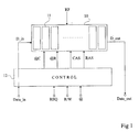
- FIG. 1 The general diagram of a system using a memory DRAM via a memory controller is shown very schematically in Figure 1.
- the indications R / W, @, REQ and D_in are provided to a control block 12 which transmits the data to be written and which basically transforms the input data into data validation of access to a row (RAS or Row Access Strobe), to validate access to a column (CAS or Column Access Strobe), row address (@R), and column address (@C).
- RAS Row Access Strobe
- CAS Column Access Strobe
- @R row address
- @C column address
- an object of the present invention is to provide a quick access management mode for reading and writing of a DRAM memory compatible in particular with the case where positioning in successive data memory is completely random, that is, it is not possible to have the data in memory in advance and / or read and write orders so that the successive data that we want to access are located in the same page (on the same row).
- the present invention aims also a memory architecture allowing such a mode of management.
- the suspend operation consists of stacking the requests in a first-in / first-out type memory.
- the method includes the steps of resuming the refresh and interrupt the succession of requests after that a determined number of interruption of refresh cycles took place.
- the memory blocks are divided into two sets accessible by parallel, from which it follows that each set has statistically to process only half of the requests.
- a memory 20 of the type DRAM according to the present invention is divided into a large number blocks (banks) of memory cells, each block 21 being associated to an address decoder (not shown), i.e. each block is coupled to a Data_in data input bus, to a Data_out data output bus, to a validation input RAS row address, to an address validation entry of CAS column, to a row address entry @R, and to a @C column address entry.
- Bus control signals are supplied by a controller 22 which receives signals D_in, REQ, R / W and @ of a user or user program by through a first-in / first-out register (FIFO) 23.
- the block 24 for, when a new address is required by the user, compare the address of the block concerned with N-1 previous block addresses, N being the number of cycles required to execute a read or write instruction. Comparison output 25 is returned to FIFO register 23 to block the last instruction and the instructions following as long as the block address at the head of the register FIFO cannot be processed.
- FIFO register 23 must be of sufficient size to contain successive instructions to form buffer in the case where several instructions designating blocks already used are sent as a result. For example, if ten instructions concerning the same block are sent sequentially, and that the processing time for an instruction is four cycles, the buffer should be able to contain thirty instructions successive.
- the first line represents CLK clock pulse cycles numbered from 1 to 14.
- the second line represents the address referred @, the first letter (in capital letters) indicating the address of a block and the second letter (in lowercase) indicating the address of a cell inside a block.
- the lines below represent the states of five memory blocks A, B, C, D, E in which readings are to be made.
- the last line represents the output data D_out. We supposes that successive readings are required addresses Aa, Bb, Cc, Dd, Ae, Ef, Cg, Ch, Bi, Aj, Nop (none operation), Dk, Fl, Gm.
- Block A is busy with this read operation at address a (reading a) for four cycles.
- Line D_out shows that at the end of cycle 4, we read DAa data. We then obtain successively on the terminal D_out the data DBb, DCc, DDd, DAe, DEf and DCg. But it's only four cycles after reading the DCg data that we can read the DCh data since instructions successive reads in block C arrived at the time cycles 7 and 8.
- a DRAM type memory requires performing periodically on each cell or rather on each row a cooling operation. This has the disadvantage that there may be a conflict between the current refresh and a read or write request requested.
- the current invention provides a solution to resolve this conflict without lose cycle time.
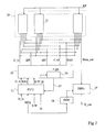
- the present invention provides to have at the input of the control circuit, at the output of the FIFO register 23 a shift register.
- this shift register is designated by the reference 31 and includes for example 2N-1 stages if the time execution of an instruction is N clock cycles. This register will include in particular the addresses of the blocks corresponding to successive requests.
- the cooling is determined by a counter 32 which increments a block number 33 and a page number for provide RFblock block and RFpage page addresses to refresh.
- the block number accessible on a bus 34 is compared with all block numbers present in register 31 with a comparator 35 whose output 36 indicates whether the block number that we want to refresh is one of the blocks that is in progress address or to be addressed during the next N cycles. If the output indicates that there is a coincidence, a block refresh logic 37 receives an inhibit signal (INHIB) refreshment. The cooling is then suspended as long as the conflict remains. When a block request problematic is executed, cooling resumes and a RF refresh request is provided by the logic block 37.
- IHIB inhibit signal
- the system includes a security mechanism to prevent cooling from being interrupted during a too long a period if the conflict remains too long, that is to say if several successive requests were addressed to the block that you want to refresh immediately considered.
- This security system includes a counter 38 which is started up at the rate of counter 32 as soon as an INHIB signal appears.
- a validation signal VAL is supplied to logic circuit 37 and this block provides a signal 39 which interrupts the progress of the system and the various pipelines to operate the cooling. The operations of read / write resume after this refresh has been made.
- a reordering register which will receive the information according to which order of execution of input requests has been modified to resend them as output in the order they were been requested.
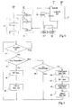
- a register 55 receives the output of the multiplexer 53 and memorizes the N requests in execution. We check in a block of Q x N comparators 56 (similar to comparator 35 of the figure 4) if the content of each of the stages of the shift register 50 corresponds to the content of one of the stages of register 55. This information is sent to logic block 54 which commands the multiplexers 52 and 53 so as to execute successively the requests corresponding to the content of the stages of the register 50 in the order of the first register whose content does not correspond not to a block stored in register 55.
- the logic circuit 54 conventionally performs other functions necessary for proper functioning of the system and in particular includes an output 57 for controlling the above-mentioned reordering register.
- the multiplexers associated with the control logic also allow the upper registers of the pipeline from the FIFO register in case the FIFO register remained empty during certain clock cycles because none request was not introduced.
- the probability of not being able to use a current cycle is equal to [(N-1) / P] Q and the probability of success is equal to 1 - [(N-1) / P] Q.
- DRAM memories of the type described above can be used together with half the number blocks previously provided in each of these memories of so as to keep total capacity unchanged, by providing two input FIFO registers. In this case, on average, half requests are sent to each memory. This gives the possibility to easily empty the input FIFO register associated with each of the memories in case it started to get fill. So the speed or bandwidth of the system is doubled. More specifically, the usable bandwidth of each memory becomes that corresponding to half the number of blocks and the bandwidth of the overall memory is double.
- the system described above only works if the memory bandwidth is not used at 100%, that is to say if we encounter absence of request (Nop) from time to time. Otherwise, the input FIFO register would fill up over time.
- Nop absence of request
- the improvement described below allows the system to operate even if a valid request is present at each clock cycle (no Nop).
- the principle is that the input FIFO register is allowed to empty faster than it fills by executing, when possible, two accesses to the memory per clock cycle. This improvement reduces the data loss rate to less than 10 -10 per cycle.
- the memory is divided into several groups of blocks. Blocks from the same group share the same bus. Each group uses a bus different from other groups. The system could work, more effectively, with one block per group, but the routing of the buses would then occupy an area very important. So we choose the grouping of blocks according to an efficiency / surface compromise.
- a control system allows two accesses to be executed in parallel, provided that the accesses belong to different block groups. The system uses a mechanism similar to that described in point 2 above in connection with a cooling mechanism for select two requests in the pipeline among the requests who are not using a previously used block. The selection of the second access uses, in addition to the criteria already described, the fact that the second access must not be in the same group of blocks as the first.
- the entire control system uses a clock double frequency to read two requests from the register FIFO while a request is made.
- the memory is divided into G groups of blocks.
- the different blocks of a group share the same address buses and data.
- a memory of 32 blocks can be organized in two groups of sixteen blocks, in four groups of eight blocks or in eight groups of four blocks.
- the organization in four groups of eight blocks will probably be the best compromise between performance and complexity (number interconnections).
- access requests in memory are stored in the input FIFO register 23 each time main clock cycle (frequency F).
- a logic circuit of execution order selection (EOS) more particularly represented in figure 8 and actuated at the frequency 2F by a secondary clock, reads a maximum of two requests from FIFO register as long as the FIFO register is not empty and it there is enough space in its Q request registers.
- Each of the two EOS outputs is sent to the block of refresh generation 64 which selects blocks that can be refreshed and when to do it without interfering with accesses in memory, as explained above. Then the requests are transferred to memory after generation of RAS and CAS signals.
- Each exit from the pipeline can be sent to any of the G blocks by through the G multiplexers (remember that the EOS has selected its outputs so that they target blocks separate).
- the EOS will be able to execute immediately all requests that are read from FIFO register so that the EOS will read a single request from the FIFO register during each main clock cycle instead two, because the FIFO register will be emptied at each cycle.
- the EOS When several consecutive requests (or almost consecutive) target the same block, in most cases the EOS will be able to reorder these requests so that at least one request can be executed at each main clock cycle.
- the invention can also be applied to memories other than DRAM memories operating on the same principle execution of a request in several clock cycles.
Landscapes
- Engineering & Computer Science (AREA)
- Microelectronics & Electronic Packaging (AREA)
- Computer Hardware Design (AREA)
- Databases & Information Systems (AREA)
- Dram (AREA)
- Advance Control (AREA)
Applications Claiming Priority (2)
| Application Number | Priority Date | Filing Date | Title |
|---|---|---|---|
| FR0101934 | 2001-02-13 | ||
| FR0101934A FR2820874B1 (fr) | 2001-02-13 | 2001-02-13 | Procede de gestion a acces aleatoire et rapide d'une memoire dram |
Publications (2)
| Publication Number | Publication Date |
|---|---|
| EP1248261A2 true EP1248261A2 (de) | 2002-10-09 |
| EP1248261A3 EP1248261A3 (de) | 2004-11-17 |
Family
ID=8859949
Family Applications (1)
| Application Number | Title | Priority Date | Filing Date |
|---|---|---|---|
| EP02354028A Withdrawn EP1248261A3 (de) | 2001-02-13 | 2002-02-11 | Random und schnelles DRAM Speicher Direktzugriffmanagementsverfahren |
Country Status (3)
| Country | Link |
|---|---|
| US (3) | US20020110038A1 (de) |
| EP (1) | EP1248261A3 (de) |
| FR (1) | FR2820874B1 (de) |
Families Citing this family (11)
| Publication number | Priority date | Publication date | Assignee | Title |
|---|---|---|---|---|
| US20050223378A1 (en) * | 2004-03-31 | 2005-10-06 | Mehmet Musa | Method and apparatus for enhancing computer application performance |
| GB2417577A (en) * | 2004-08-25 | 2006-03-01 | Imagination Tech Ltd | Memory controller with randomised bank selection |
| US20060129740A1 (en) * | 2004-12-13 | 2006-06-15 | Hermann Ruckerbauer | Memory device, memory controller and method for operating the same |
| US20070150697A1 (en) * | 2005-05-10 | 2007-06-28 | Telairity Semiconductor, Inc. | Vector processor with multi-pipe vector block matching |
| JP4772546B2 (ja) | 2006-03-17 | 2011-09-14 | 富士通セミコンダクター株式会社 | 半導体メモリ、メモリシステムおよびメモリシステムの動作方法 |
| US9208835B2 (en) | 2009-12-29 | 2015-12-08 | Micron Technology, Inc. | Timing violation handling in a synchronous interface memory |
| US8649238B2 (en) * | 2010-04-02 | 2014-02-11 | Samsung Electronics Co., Ltd. | Semiconductor memory device and method of controlling the same |
| US9665432B2 (en) | 2014-08-07 | 2017-05-30 | Microsoft Technology Licensing, Llc | Safe data access following storage failure |
| US9847918B2 (en) | 2014-08-12 | 2017-12-19 | Microsoft Technology Licensing, Llc | Distributed workload reassignment following communication failure |
| KR102373544B1 (ko) | 2015-11-06 | 2022-03-11 | 삼성전자주식회사 | 요청 기반의 리프레쉬를 수행하는 메모리 장치, 메모리 시스템 및 메모리 장치의 동작방법 |
| US11080183B2 (en) | 2019-08-13 | 2021-08-03 | Elite Semiconductor Memory Technology Inc. | Memory chip, memory module and method for pseudo-accessing memory bank thereof |
Family Cites Families (19)
| Publication number | Priority date | Publication date | Assignee | Title |
|---|---|---|---|---|
| US29364A (en) * | 1860-07-31 | Wabming apparatus | ||
| JPS6356754A (ja) * | 1986-08-28 | 1988-03-11 | Toshiba Corp | 入出力チヤネル |
| FR2632093B1 (fr) * | 1988-05-25 | 1990-08-10 | Bull Sa | Memoire modulaire |
| US4937791A (en) * | 1988-06-02 | 1990-06-26 | The California Institute Of Technology | High performance dynamic ram interface |
| JP2628588B2 (ja) | 1989-12-11 | 1997-07-09 | シャープ株式会社 | Dramのリフレッシュ回路 |
| JPH07122864B2 (ja) * | 1991-07-22 | 1995-12-25 | インターナショナル・ビジネス・マシーンズ・コーポレイション | データ処理システム、データ処理システムに使用するインターフエース回路及びデータ・プロセツサ間の通信方法 |
| EP0591695B1 (de) * | 1992-09-18 | 1998-02-11 | Hitachi, Ltd. | Rechenanlage mit synchronem, dynamischem Speicher |
| JP2637931B2 (ja) * | 1994-12-01 | 1997-08-06 | インターナショナル・ビジネス・マシーンズ・コーポレイション | テクスチャ・マッピングを行うコンピュータ・システム |
| JPH09288614A (ja) * | 1996-04-22 | 1997-11-04 | Mitsubishi Electric Corp | 半導体集積回路装置、半導体記憶装置およびそのための制御回路 |
| US6016504A (en) * | 1996-08-28 | 2000-01-18 | Infospace.Com, Inc. | Method and system for tracking the purchase of a product and services over the Internet |
| US6229752B1 (en) * | 1997-02-17 | 2001-05-08 | Hitachi, Ltd. | Semiconductor integrated circuit device |
| US6370073B2 (en) * | 1998-10-01 | 2002-04-09 | Monlithic System Technology, Inc. | Single-port multi-bank memory system having read and write buffers and method of operating same |
| JP2000163956A (ja) * | 1998-11-24 | 2000-06-16 | Sharp Corp | 半導体記憶装置 |
| US20020002513A1 (en) * | 1998-11-25 | 2002-01-03 | James P. Chiasson | Computer network transaction system |
| KR100287188B1 (ko) * | 1999-04-06 | 2001-04-16 | 윤종용 | 데이터 처리속도 및 데이터 입출력핀의 효율을 향상시킬 수 있는 반도체 메모리장치 및 이의 독출기입 제어방법 |
| AU2284301A (en) | 2000-01-03 | 2001-07-16 | Icoding Technology, Inc. | System and method for high speed processing of turbo codes |
| US6741256B2 (en) * | 2001-08-27 | 2004-05-25 | Sun Microsystems, Inc. | Predictive optimizer for DRAM memory |
| US6560155B1 (en) * | 2001-10-24 | 2003-05-06 | Micron Technology, Inc. | System and method for power saving memory refresh for dynamic random access memory devices after an extended interval |
| FR2835425B1 (fr) * | 2002-02-04 | 2004-04-09 | Tornier Sa | Element prothetique comprenant deux composants et procede d'assemblage d'un tel element prothetique |
-
2001
- 2001-02-13 FR FR0101934A patent/FR2820874B1/fr not_active Expired - Fee Related
-
2002
- 2002-02-11 EP EP02354028A patent/EP1248261A3/de not_active Withdrawn
- 2002-02-13 US US10/075,001 patent/US20020110038A1/en not_active Abandoned
-
2003
- 2003-09-22 US US10/668,060 patent/US20040133730A1/en not_active Abandoned
-
2006
- 2006-11-08 US US11/594,689 patent/US7436728B2/en not_active Expired - Fee Related
Also Published As
| Publication number | Publication date |
|---|---|
| US20070186030A1 (en) | 2007-08-09 |
| FR2820874B1 (fr) | 2003-05-30 |
| FR2820874A1 (fr) | 2002-08-16 |
| US7436728B2 (en) | 2008-10-14 |
| EP1248261A3 (de) | 2004-11-17 |
| US20020110038A1 (en) | 2002-08-15 |
| US20040133730A1 (en) | 2004-07-08 |
Similar Documents
| Publication | Publication Date | Title |
|---|---|---|
| EP2366147B1 (de) | Physischer manager der synchronisationsbarriere zwischen mehreren prozessen | |
| FR2778258A1 (fr) | Controleur d'acces de trafic dans une memoire, systeme de calcul comprenant ce controleur d'acces et procede de fonctionnement d'un tel controleur d'acces | |
| EP1248261A2 (de) | Random und schnelles DRAM Speicher Direktzugriffmanagementsverfahren | |
| US20080228991A1 (en) | Ring buffer management | |
| FR2881540A1 (fr) | Procede et systeme destines a empecher que des lignes de memoire cache soient videes jusqu'a ce que les donnees stockees dans celles-ci ne soient utilisees. | |
| TW200929212A (en) | Memory device and refresh method thereof | |
| EP3182292B1 (de) | Verfahren zur vorhersage einer dateninformation, die vorab in einen cache-speicher geladen werden muss | |
| EP0392932B1 (de) | Verfahren und Vorrichtung zur Speicherzugriffsbeschleunigung unter Verwendung eines modifizierten LRU-Algorithmus | |
| FR3032814A1 (de) | ||
| WO2003038620A2 (fr) | Procede de memorisation de donnees avec correction d'erreur | |
| FR2797969A1 (fr) | Dispositif a plusieurs processeurs partageant une memoire collective | |
| EP4435615B1 (de) | Verfahren zur verwaltung eines cache-speichers | |
| CN102567243B (zh) | 存储设备的刷新处理方法和存储设备 | |
| EP0394115A1 (de) | Vorrichtung zur Speicherzugriffsbeschleunigung in einer Datenverarbeitungsanlage | |
| FR2625342A1 (fr) | Dispositif permettant de traiter simultanement les demandes de transfert produites par l'unite centrale de traitement, l'unite de traitement arithmetique et l'unite de traitement d'entree-sortie d'un ordinateur de grande puissance | |
| CN107783909A (zh) | 一种内存地址总线扩展方法及装置 | |
| FR2801388A1 (fr) | Procede de commande de memoire dram rapide et controleur adapte | |
| US11837271B2 (en) | Memory control apparatus and control method therefor | |
| EP2043103A2 (de) | Elektronische Speichervorrichtung | |
| FR2800551A1 (fr) | Decodeur mpeg utilisant une memoire partagee | |
| CN116257191A (zh) | 存储器的控制器、组件、电子设备及命令调度方法 | |
| EP1632863B1 (de) | Programmierbare Vorrichtung für einer Steuerschnittstelle. | |
| FR2797970A1 (fr) | Adressage d'une memoire | |
| FR2797971A1 (fr) | Acces a une ressource collective | |
| FR2779541A1 (fr) | Acces rapide aux circuits tampons |
Legal Events
| Date | Code | Title | Description |
|---|---|---|---|
| PUAI | Public reference made under article 153(3) epc to a published international application that has entered the european phase |
Free format text: ORIGINAL CODE: 0009012 |
|
| AK | Designated contracting states |
Kind code of ref document: A2 Designated state(s): AT BE CH CY DE DK ES FI FR GB GR IE IT LI LU MC NL PT SE TR |
|
| AX | Request for extension of the european patent |
Free format text: AL;LT;LV;MK;RO;SI |
|
| PUAL | Search report despatched |
Free format text: ORIGINAL CODE: 0009013 |
|
| AK | Designated contracting states |
Kind code of ref document: A3 Designated state(s): AT BE CH CY DE DK ES FI FR GB GR IE IT LI LU MC NL PT SE TR |
|
| AX | Request for extension of the european patent |
Extension state: AL LT LV MK RO SI |
|
| 17P | Request for examination filed |
Effective date: 20050517 |
|
| AKX | Designation fees paid |
Designated state(s): DE FR GB IT |
|
| STAA | Information on the status of an ep patent application or granted ep patent |
Free format text: STATUS: THE APPLICATION IS DEEMED TO BE WITHDRAWN |
|
| 18D | Application deemed to be withdrawn |
Effective date: 20120901 |