EP1249869A2 - Arrangement pour le refroidissement d'un dispositif semiconducteur de puissance - Google Patents
Arrangement pour le refroidissement d'un dispositif semiconducteur de puissance Download PDFInfo
- Publication number
- EP1249869A2 EP1249869A2 EP02008005A EP02008005A EP1249869A2 EP 1249869 A2 EP1249869 A2 EP 1249869A2 EP 02008005 A EP02008005 A EP 02008005A EP 02008005 A EP02008005 A EP 02008005A EP 1249869 A2 EP1249869 A2 EP 1249869A2
- Authority
- EP
- European Patent Office
- Prior art keywords
- power semiconductor
- insulating layer
- layer
- semiconductor element
- arrangement according
- Prior art date
- Legal status (The legal status is an assumption and is not a legal conclusion. Google has not performed a legal analysis and makes no representation as to the accuracy of the status listed.)
- Withdrawn
Links
Images
Classifications
-
- H—ELECTRICITY
- H05—ELECTRIC TECHNIQUES NOT OTHERWISE PROVIDED FOR
- H05K—PRINTED CIRCUITS; CASINGS OR CONSTRUCTIONAL DETAILS OF ELECTRIC APPARATUS; MANUFACTURE OF ASSEMBLAGES OF ELECTRICAL COMPONENTS
- H05K1/00—Printed circuits
- H05K1/02—Details
- H05K1/03—Use of materials for the substrate
- H05K1/05—Insulated conductive substrates, e.g. insulated metal substrate
- H05K1/053—Insulated conductive substrates, e.g. insulated metal substrate the metal substrate being covered by an inorganic insulating layer
-
- H—ELECTRICITY
- H10—SEMICONDUCTOR DEVICES; ELECTRIC SOLID-STATE DEVICES NOT OTHERWISE PROVIDED FOR
- H10W—GENERIC PACKAGES, INTERCONNECTIONS, CONNECTORS OR OTHER CONSTRUCTIONAL DETAILS OF DEVICES COVERED BY CLASS H10
- H10W40/00—Arrangements for thermal protection or thermal control
- H10W40/20—Arrangements for cooling
- H10W40/25—Arrangements for cooling characterised by their materials
- H10W40/255—Arrangements for cooling characterised by their materials having a laminate or multilayered structure, e.g. direct bond copper [DBC] ceramic substrates
-
- H—ELECTRICITY
- H10—SEMICONDUCTOR DEVICES; ELECTRIC SOLID-STATE DEVICES NOT OTHERWISE PROVIDED FOR
- H10W—GENERIC PACKAGES, INTERCONNECTIONS, CONNECTORS OR OTHER CONSTRUCTIONAL DETAILS OF DEVICES COVERED BY CLASS H10
- H10W70/00—Package substrates; Interposers; Redistribution layers [RDL]
- H10W70/60—Insulating or insulated package substrates; Interposers; Redistribution layers
- H10W70/62—Insulating or insulated package substrates; Interposers; Redistribution layers characterised by their interconnections
- H10W70/66—Conductive materials thereof
- H10W70/666—Organic materials or pastes
-
- H—ELECTRICITY
- H10—SEMICONDUCTOR DEVICES; ELECTRIC SOLID-STATE DEVICES NOT OTHERWISE PROVIDED FOR
- H10W—GENERIC PACKAGES, INTERCONNECTIONS, CONNECTORS OR OTHER CONSTRUCTIONAL DETAILS OF DEVICES COVERED BY CLASS H10
- H10W90/00—Package configurations
-
- H—ELECTRICITY
- H10—SEMICONDUCTOR DEVICES; ELECTRIC SOLID-STATE DEVICES NOT OTHERWISE PROVIDED FOR
- H10W—GENERIC PACKAGES, INTERCONNECTIONS, CONNECTORS OR OTHER CONSTRUCTIONAL DETAILS OF DEVICES COVERED BY CLASS H10
- H10W72/00—Interconnections or connectors in packages
- H10W72/071—Connecting or disconnecting
- H10W72/075—Connecting or disconnecting of bond wires
-
- H—ELECTRICITY
- H10—SEMICONDUCTOR DEVICES; ELECTRIC SOLID-STATE DEVICES NOT OTHERWISE PROVIDED FOR
- H10W—GENERIC PACKAGES, INTERCONNECTIONS, CONNECTORS OR OTHER CONSTRUCTIONAL DETAILS OF DEVICES COVERED BY CLASS H10
- H10W72/00—Interconnections or connectors in packages
- H10W72/50—Bond wires
- H10W72/531—Shapes of wire connectors
- H10W72/5363—Shapes of wire connectors the connected ends being wedge-shaped
-
- H—ELECTRICITY
- H10—SEMICONDUCTOR DEVICES; ELECTRIC SOLID-STATE DEVICES NOT OTHERWISE PROVIDED FOR
- H10W—GENERIC PACKAGES, INTERCONNECTIONS, CONNECTORS OR OTHER CONSTRUCTIONAL DETAILS OF DEVICES COVERED BY CLASS H10
- H10W72/00—Interconnections or connectors in packages
- H10W72/50—Bond wires
- H10W72/551—Materials of bond wires
-
- H—ELECTRICITY
- H10—SEMICONDUCTOR DEVICES; ELECTRIC SOLID-STATE DEVICES NOT OTHERWISE PROVIDED FOR
- H10W—GENERIC PACKAGES, INTERCONNECTIONS, CONNECTORS OR OTHER CONSTRUCTIONAL DETAILS OF DEVICES COVERED BY CLASS H10
- H10W72/00—Interconnections or connectors in packages
- H10W72/90—Bond pads, in general
- H10W72/951—Materials of bond pads
Definitions
- the invention relates to an arrangement for cooling a Power semiconductor element.
- Heat is mostly used in aluminum heat sinks. Is to a good heat-conducting connection between the power semiconductor element and the heat sink required, in which As a rule, additional electrical insulation is required. Around the thermal resistance between the power semiconductor element and Keeping the heat sink as low as possible are different Pastes and adhesives, which are also conductive if necessary, known. Nevertheless, the heat transfer media have the largest share in the thermal resistance of the entire structure.
- the object of the present invention is a good one Heat transfer between the power semiconductor element and the Heatsink while maintaining reliable electrical Ensure insulation.
- This object is achieved in that on a Aluminum carrier an insulating layer made of ceramic material is applied, on which the power semiconductor element is arranged.
- the insulating layer is preferably included applied a plasma chemical process.
- a Layer thickness of preferably 5 ⁇ m to 30 ⁇ m enables a adequate electrical insulation with the lowest possible Thermal resistance.
- An advantageous embodiment of the arrangement according to the invention is that the power semiconductor element on a conductive layer is arranged on the insulating layer.
- the conductive layer can be a usual directly - for example by Screen printing or dosing - or indirectly with peel-off film applied track.
- further conductor tracks can also be provided.
- the arrangement according to the invention has the advantage of a better one thermal connection of the power semiconductor element to the Heatsink and thus a reduction in thermal resistance. It can with the same performance requirements smaller and therefore more cost-effective power semiconductor elements are used.
- the invention further enables a mix between Standard electronics and direct layer on aluminum, whereby for Connection thick wire bonding is suitable.
- the conductive layer with melting at low temperatures Thick-film pastes or with an electrically conductive adhesive is made.
- the arrangement according to the invention can also go further be formed that further on the insulating layer Film resistors are arranged, made of polymer pastes consist.
- the invention permits numerous embodiments. One of those is shown schematically in the drawing and below described.
- the drawing shows the exemplary embodiment schematically, the layers are stronger than because of the better recognizability are actually depicted.
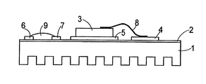
- Aluminum is an insulating layer 2 made of ceramic applied.
- the conductor track 5 carries the power semiconductor element 3, the electric one hand - preferably by soldering - with the conductor track 5 and on the other hand via one Bond wire 8 is connected to the conductor track 4.
- the further conductor tracks 6 and 7 are via a thick-film resistor 9 connected to each other.
Landscapes
- Chemical & Material Sciences (AREA)
- Inorganic Chemistry (AREA)
- Engineering & Computer Science (AREA)
- Microelectronics & Electronic Packaging (AREA)
- Cooling Or The Like Of Semiconductors Or Solid State Devices (AREA)
Applications Claiming Priority (2)
| Application Number | Priority Date | Filing Date | Title |
|---|---|---|---|
| DE10118384A DE10118384A1 (de) | 2001-04-12 | 2001-04-12 | Anordnung zur Kühlung eines Leistungs-Halbleiterelementes |
| DE10118384 | 2001-04-12 |
Publications (2)
| Publication Number | Publication Date |
|---|---|
| EP1249869A2 true EP1249869A2 (fr) | 2002-10-16 |
| EP1249869A3 EP1249869A3 (fr) | 2006-05-17 |
Family
ID=7681438
Family Applications (1)
| Application Number | Title | Priority Date | Filing Date |
|---|---|---|---|
| EP02008005A Withdrawn EP1249869A3 (fr) | 2001-04-12 | 2002-04-10 | Arrangement pour le refroidissement d'un dispositif semiconducteur de puissance |
Country Status (2)
| Country | Link |
|---|---|
| EP (1) | EP1249869A3 (fr) |
| DE (1) | DE10118384A1 (fr) |
Cited By (3)
| Publication number | Priority date | Publication date | Assignee | Title |
|---|---|---|---|---|
| EP1659838A3 (fr) * | 2004-10-27 | 2007-03-07 | Brother Kogyo Kabushiki Kaisha | Substrat avec des composants montés en surface, élément de conductivité thermique pour ledit substrat, et tête d'éjection de liquide |
| EP1622198A3 (fr) * | 2004-07-28 | 2007-04-11 | Brother Kogyo Kabushiki Kaisha | Substrat avec composant électronique et tête d'éjection de liquide avec ce substrat |
| US7453145B2 (en) * | 2002-07-08 | 2008-11-18 | Siemens Aktiengesellschaft | Electronics unit |
Families Citing this family (3)
| Publication number | Priority date | Publication date | Assignee | Title |
|---|---|---|---|---|
| DE102004018475A1 (de) * | 2004-04-16 | 2005-11-10 | eupec Europäische Gesellschaft für Leistungshalbleiter mbH | Leistungshalbleiteranordnung |
| DE102004055534B4 (de) * | 2004-11-17 | 2017-10-05 | Danfoss Silicon Power Gmbh | Leistungshalbleitermodul mit einer elektrisch isolierenden und thermisch gut leitenden Schicht |
| DE102008005747A1 (de) * | 2008-01-24 | 2009-07-30 | Bayerische Motoren Werke Aktiengesellschaft | Leistungselektronikmodul |
Citations (1)
| Publication number | Priority date | Publication date | Assignee | Title |
|---|---|---|---|---|
| DE19641397A1 (de) * | 1996-09-27 | 1998-04-02 | Siemens Ag | Verfahren zum Herstellen einer wärmeableitenden Leiterplatte |
Family Cites Families (7)
| Publication number | Priority date | Publication date | Assignee | Title |
|---|---|---|---|---|
| DE3523061A1 (de) * | 1985-06-27 | 1987-01-02 | Siemens Ag | Halbleiter-chip-anordnung |
| EP0221531A3 (fr) * | 1985-11-06 | 1992-02-19 | Kanegafuchi Kagaku Kogyo Kabushiki Kaisha | Substrat isolé bon conducteur de chaleur et procédé pour sa fabrication |
| DE8908678U1 (de) * | 1989-07-17 | 1990-11-15 | Siemens AG, 1000 Berlin und 8000 München | Leistungsbaugruppe |
| DE8914493U1 (de) * | 1989-12-08 | 1990-05-17 | Siemens AG, 1000 Berlin und 8000 München | Leistungsbaugruppe |
| FR2689315A1 (fr) * | 1992-03-27 | 1993-10-01 | Alsthom Cge Alcatel | Procédé de fabrication d'un substrat pour l'électronique de puissance et substrat obtenu par ce procédé. |
| KR19990028818A (ko) * | 1995-07-14 | 1999-04-15 | 와인스타인 폴 | 금속 볼 그리드 전자 패키지 |
| DE19722355A1 (de) * | 1997-05-28 | 1998-12-03 | Bosch Gmbh Robert | Verfahren zur Herstellung elektrischer Baugruppen und elektrische Baugruppe |
-
2001
- 2001-04-12 DE DE10118384A patent/DE10118384A1/de not_active Withdrawn
-
2002
- 2002-04-10 EP EP02008005A patent/EP1249869A3/fr not_active Withdrawn
Patent Citations (1)
| Publication number | Priority date | Publication date | Assignee | Title |
|---|---|---|---|---|
| DE19641397A1 (de) * | 1996-09-27 | 1998-04-02 | Siemens Ag | Verfahren zum Herstellen einer wärmeableitenden Leiterplatte |
Cited By (6)
| Publication number | Priority date | Publication date | Assignee | Title |
|---|---|---|---|---|
| US7453145B2 (en) * | 2002-07-08 | 2008-11-18 | Siemens Aktiengesellschaft | Electronics unit |
| EP1622198A3 (fr) * | 2004-07-28 | 2007-04-11 | Brother Kogyo Kabushiki Kaisha | Substrat avec composant électronique et tête d'éjection de liquide avec ce substrat |
| US7352591B2 (en) | 2004-07-28 | 2008-04-01 | Brother Kogyo Kabushiki Kaisha | Substrate mounted with electronic element thereon and liquid ejection head including the substrate |
| US7558071B2 (en) | 2004-07-28 | 2009-07-07 | Brother Kogyo Kabushiki Kaisha | Substrate mounted with electronic element thereon |
| EP1659838A3 (fr) * | 2004-10-27 | 2007-03-07 | Brother Kogyo Kabushiki Kaisha | Substrat avec des composants montés en surface, élément de conductivité thermique pour ledit substrat, et tête d'éjection de liquide |
| US7286354B2 (en) | 2004-10-27 | 2007-10-23 | Brother Kogyo Kabushiki Kaisha | Electronic part-mounted substrate, thermal conductive member for electronic part-mounted substrate and liquid-jetting head |
Also Published As
| Publication number | Publication date |
|---|---|
| DE10118384A1 (de) | 2002-10-24 |
| EP1249869A3 (fr) | 2006-05-17 |
Similar Documents
| Publication | Publication Date | Title |
|---|---|---|
| DE112014001487B4 (de) | Halbleitermodul | |
| DE102008048005B3 (de) | Leistungshalbleitermodulanordnung und Verfahren zur Herstellung einer Leistungshalbleitermodulanordnung | |
| DE19617055C1 (de) | Halbleiterleistungsmodul hoher Packungsdichte in Mehrschichtbauweise | |
| EP0931346B1 (fr) | Composant microelectronique a structure sandwich | |
| DE3782646T2 (de) | Vorrichtung und verfahren zur verbindung von schaltungspackungen. | |
| DE102005039478A1 (de) | Leistungshalbleiterbauteil mit Halbleiterchipstapel und Verfahren zur Herstellung desselben | |
| DE212021000109U1 (de) | Halbleiterbauteil | |
| EP1445799A2 (fr) | Dispositif à dissipation de chaleur pour un semi-conducteur sur un circuit imprimé | |
| EP0264364B1 (fr) | Appareil de commutation electrique | |
| EP0535414A2 (fr) | Dispositif de circuit électronique | |
| WO1992006496A1 (fr) | Circuits hybrides multicouches avec composants de puissance | |
| WO2010018466A2 (fr) | Dispositif, en particulier pour conduire du courant, et procédé de fabrication d'un dispositif, en particulier pour conduire du courant | |
| DE10212449A1 (de) | Träger für eine elektrische Schaltung, insbesondere für einen elektrischen Schalter | |
| EP1249869A2 (fr) | Arrangement pour le refroidissement d'un dispositif semiconducteur de puissance | |
| DE3444699C2 (fr) | ||
| DE4017181C2 (de) | Elektrisches Bauelement | |
| DE3930858A1 (de) | Modulaufbau | |
| DE202019106541U1 (de) | Leistungsmodul mit gehäusten Leistungshalbleitern zur steuerbaren elektrischen Leistungsversorgung eines Verbrauchers | |
| DE102019218157A1 (de) | Leistungsmodul mit gehäusten Leistungshalbleitern zur steuerbaren elektrischen Leistungsversorgung eines Verbrauchers sowie Verfahren zur Herstellung | |
| WO2014146830A1 (fr) | Module de puissance ayant au moins un composant de puissance | |
| EP0555668B1 (fr) | Plaquette à circuit imprimé pour un circuit électronique de puissance contenant des semiconducteurs à grande puissance | |
| EP2704194A1 (fr) | Module semi-conducteur de puissance et procédé de fabrication d'un module semi-conducteur de puissance | |
| DE102017217406A1 (de) | Bauelement und Verfahren zu dessen Herstellung | |
| EP4211996A1 (fr) | Procédé et système de production de pièce coulée pour la production d'un carter de moteur électrique, et moteur électrique | |
| DE10217214B4 (de) | Kühlanordnung für eine Schaltungsanordnung |
Legal Events
| Date | Code | Title | Description |
|---|---|---|---|
| PUAI | Public reference made under article 153(3) epc to a published international application that has entered the european phase |
Free format text: ORIGINAL CODE: 0009012 |
|
| AK | Designated contracting states |
Kind code of ref document: A2 Designated state(s): AT BE CH CY DE DK ES FI FR GB GR IE IT LI LU MC NL PT SE TR |
|
| AX | Request for extension of the european patent |
Free format text: AL;LT;LV;MK;RO;SI |
|
| PUAL | Search report despatched |
Free format text: ORIGINAL CODE: 0009013 |
|
| AK | Designated contracting states |
Kind code of ref document: A3 Designated state(s): AT BE CH CY DE DK ES FI FR GB GR IE IT LI LU MC NL PT SE TR |
|
| AX | Request for extension of the european patent |
Extension state: AL LT LV MK RO SI |
|
| RIC1 | Information provided on ipc code assigned before grant |
Ipc: H01L 25/16 20060101ALI20060327BHEP Ipc: H01L 23/498 20060101ALI20060327BHEP Ipc: H01L 23/373 20060101AFI20020802BHEP Ipc: H05K 1/05 20060101ALI20060327BHEP |
|
| 17P | Request for examination filed |
Effective date: 20061023 |
|
| AKX | Designation fees paid |
Designated state(s): DE FR GB |
|
| 17Q | First examination report despatched |
Effective date: 20070205 |
|
| RAP1 | Party data changed (applicant data changed or rights of an application transferred) |
Owner name: CONTINENTAL AUTOMOTIVE GMBH |
|
| STAA | Information on the status of an ep patent application or granted ep patent |
Free format text: STATUS: THE APPLICATION IS DEEMED TO BE WITHDRAWN |
|
| 18D | Application deemed to be withdrawn |
Effective date: 20180605 |
|
| RIC1 | Information provided on ipc code assigned before grant |
Ipc: H05K 1/05 20060101ALI20060327BHEP Ipc: H01L 23/373 20060101AFI20020802BHEP Ipc: H01L 25/16 20060101ALI20060327BHEP Ipc: H01L 23/498 20060101ALI20060327BHEP |