EP1249902A2 - Optical semiconductor module - Google Patents
Optical semiconductor module Download PDFInfo
- Publication number
- EP1249902A2 EP1249902A2 EP02008017A EP02008017A EP1249902A2 EP 1249902 A2 EP1249902 A2 EP 1249902A2 EP 02008017 A EP02008017 A EP 02008017A EP 02008017 A EP02008017 A EP 02008017A EP 1249902 A2 EP1249902 A2 EP 1249902A2
- Authority
- EP
- European Patent Office
- Prior art keywords
- laser diode
- semiconductor laser
- substrate
- active layer
- semiconductor module
- Prior art date
- Legal status (The legal status is an assumption and is not a legal conclusion. Google has not performed a legal analysis and makes no representation as to the accuracy of the status listed.)
- Granted
Links
Images


Classifications
-
- H—ELECTRICITY
- H01—ELECTRIC ELEMENTS
- H01S—DEVICES USING THE PROCESS OF LIGHT AMPLIFICATION BY STIMULATED EMISSION OF RADIATION [LASER] TO AMPLIFY OR GENERATE LIGHT; DEVICES USING STIMULATED EMISSION OF ELECTROMAGNETIC RADIATION IN WAVE RANGES OTHER THAN OPTICAL
- H01S5/00—Semiconductor lasers
- H01S5/02—Structural details or components not essential to laser action
- H01S5/022—Mountings; Housings
- H01S5/0235—Method for mounting laser chips
- H01S5/02355—Fixing laser chips on mounts
- H01S5/0237—Fixing laser chips on mounts by soldering
-
- H—ELECTRICITY
- H01—ELECTRIC ELEMENTS
- H01S—DEVICES USING THE PROCESS OF LIGHT AMPLIFICATION BY STIMULATED EMISSION OF RADIATION [LASER] TO AMPLIFY OR GENERATE LIGHT; DEVICES USING STIMULATED EMISSION OF ELECTROMAGNETIC RADIATION IN WAVE RANGES OTHER THAN OPTICAL
- H01S5/00—Semiconductor lasers
- H01S5/02—Structural details or components not essential to laser action
- H01S5/022—Mountings; Housings
- H01S5/0233—Mounting configuration of laser chips
- H01S5/0234—Up-side down mountings, e.g. Flip-chip, epi-side down mountings or junction down mountings
-
- H—ELECTRICITY
- H10—SEMICONDUCTOR DEVICES; ELECTRIC SOLID-STATE DEVICES NOT OTHERWISE PROVIDED FOR
- H10W—GENERIC PACKAGES, INTERCONNECTIONS, CONNECTORS OR OTHER CONSTRUCTIONAL DETAILS OF DEVICES COVERED BY CLASS H10
- H10W72/00—Interconnections or connectors in packages
- H10W72/30—Die-attach connectors
-
- H—ELECTRICITY
- H01—ELECTRIC ELEMENTS
- H01S—DEVICES USING THE PROCESS OF LIGHT AMPLIFICATION BY STIMULATED EMISSION OF RADIATION [LASER] TO AMPLIFY OR GENERATE LIGHT; DEVICES USING STIMULATED EMISSION OF ELECTROMAGNETIC RADIATION IN WAVE RANGES OTHER THAN OPTICAL
- H01S5/00—Semiconductor lasers
- H01S5/02—Structural details or components not essential to laser action
- H01S5/022—Mountings; Housings
- H01S5/0233—Mounting configuration of laser chips
- H01S5/02345—Wire-bonding
-
- H—ELECTRICITY
- H01—ELECTRIC ELEMENTS
- H01S—DEVICES USING THE PROCESS OF LIGHT AMPLIFICATION BY STIMULATED EMISSION OF RADIATION [LASER] TO AMPLIFY OR GENERATE LIGHT; DEVICES USING STIMULATED EMISSION OF ELECTROMAGNETIC RADIATION IN WAVE RANGES OTHER THAN OPTICAL
- H01S5/00—Semiconductor lasers
- H01S5/04—Processes or apparatus for excitation, e.g. pumping, e.g. by electron beams
- H01S5/042—Electrical excitation ; Circuits therefor
- H01S5/0425—Electrodes, e.g. characterised by the structure
- H01S5/04256—Electrodes, e.g. characterised by the structure characterised by the configuration
-
- H—ELECTRICITY
- H01—ELECTRIC ELEMENTS
- H01S—DEVICES USING THE PROCESS OF LIGHT AMPLIFICATION BY STIMULATED EMISSION OF RADIATION [LASER] TO AMPLIFY OR GENERATE LIGHT; DEVICES USING STIMULATED EMISSION OF ELECTROMAGNETIC RADIATION IN WAVE RANGES OTHER THAN OPTICAL
- H01S5/00—Semiconductor lasers
- H01S5/20—Structure or shape of the semiconductor body to guide the optical wave ; Confining structures perpendicular to the optical axis, e.g. index or gain guiding, stripe geometry, broad area lasers, gain tailoring, transverse or lateral reflectors, special cladding structures, MQW barrier reflection layers
- H01S5/22—Structure or shape of the semiconductor body to guide the optical wave ; Confining structures perpendicular to the optical axis, e.g. index or gain guiding, stripe geometry, broad area lasers, gain tailoring, transverse or lateral reflectors, special cladding structures, MQW barrier reflection layers having a ridge or stripe structure
- H01S5/227—Buried mesa structure ; Striped active layer
- H01S5/2275—Buried mesa structure ; Striped active layer mesa created by etching
- H01S5/2277—Buried mesa structure ; Striped active layer mesa created by etching double channel planar buried heterostructure [DCPBH] laser
Definitions
- the invention relates to an optical semiconductor module on which a laser diode is mounted, and especially to an optical semiconductor module in which a semiconductor laser diode is fixed to a substrate by soldering.
- the optical semiconductor module on which a laser diode is mounted is widely used as a light source in the field of the optical communication.
- the semiconductor laser diode is fixed to the substrate having the high heat conductivity, and an optical fiber is optically coupled with the optical semiconductor module by adjusting the position of the core of the optical fiber relative to the semiconductor laser diode.
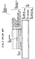
- FIG.1 shows an outline of the structure of the conventional semiconductor laser diode.
- the semiconductor laser diode 21 of the distributed feedback type or the Fabry-Perot type is composed of a substrate 22 and plural layers 23 (shown as a single layer in FIG. 1 for simplicity) which are formed on the substrate 22 and includes an active layer for outputting laser light.
- the thickness of the plural layers 23 can be precisely controlled, because those are formed by the epitaxial growth.
- the substrate 22 serving as a pedestal of the plural layers 23 is formed of InGaAs etc., and is processed by machining; the thickness of the substrate 22 is no so accurate as that of the plural layers 23.
- the substrate 22 of the semiconductor laser diode 21 is situated on the reference plane (not shown), it becomes difficult to adjust the core of the optical fiber (not shown), the position of which is determined based on the same reference plane, to the light-emitting region 24 formed in the plural layers 23.
- FIG. 2 shows an important part of the other example of such an optical semiconductor module, which is disclosed in Japanese Patent Applications, Laid-Open, H09-064479.
- a heat sink top surface electrode 33 is formed on the top surface of a heat sink member 32, and a heat sink bottom surface electrode 34 is formed on the bottom surface of the same.
- the heat sink top and bottom surface electrodes 33, 34, and the heat sink member 32 form a heat sink 35.
- a semiconductor laser diode 36 is mounted on the heat sink 35 by means of a solder layer 37 formed of AuSn.
- a GaAs substrate 39 serves as the basic material thereof, and the reverse surface of the GaAs substrate 39 is covered with an electrode 38 formed of Au.
- an active layer 40 having the light-emitting function is formed by the epitaxial growth, and a light-emitting region 41 is formed in the middle of the active layer 40.
- a cap layer 42 is formed by the epitaxial growth; and an ohmic electrode layer 43, a non-alloyed electrode layer 44, and an alloyed electrode layer 45 are successively formed on the bottom surface of the cap layer 42, where the alloyed electrode layer 45 tightly adheres to the solder layer 37, because an alloy layer is formed therebetween.
- FIG.3 shows a bottom view of the semiconductor laser diode 31, which is fixed to the top surface of the heat sink 35 by soldering.
- the alloyed electrode layer 45 is separated into two parts, which are arranged symmetrically with respect to the vertical bisector of the semiconductor laser diode 31, leaving a predetermined width 51 therebetween.
- the vertical bisector mentioned in the above coincides with a projection of the central axis of the light-emitting region 41.
- the solder layer 37 fits into a space 52 formed by the bottom surface of the non-alloyed electrode layer 44 and both the inner side edges of the alloyed electrode layer 45 separated into the two parts.
- the semiconductor laser diode of the distributed feed back type since the diffraction grating in the active layer, which is united with the light-emitting region 41, is deformed, and the refractive index of the active layer changes because of the stress exerted thereon; there arises the apprehension that the lasign wavelength of the laser light will shift from the intrinsic one to the other one on account of the change of the current or the ambient temperature, or the side mode level will increases, so that it becomes difficult to keep a stable operation based on the single mode.
- the proposal shown in FIGs. 2 to 3 since melted solder may flow into a domain situated just under the light emitting region, there is a possibility that the aforementioned problems will be actualized.
- the semiconductor laser diode of the Fabry-Perot type is not so seriously affected by the aforementioned problems, the quality of the laser light is deteriorated because of the deformation of mirrors forming the light emitting region 41 in common with the semiconductor laser diode of the distributed feedback type.
- an object of the invention to provide an optical semiconductor module, in which a distortion of or a residual stress exerted on an active layer formed in a semiconductor laser diode can be minimized, when a bottom surface of a semiconductor diode overspreading an active layer is fixed to a top surface of a substrate by soldering.
- an optical semiconductor module comprises:
- solder layers are situated so that the vacant space is formed just under the active layer, when the semiconductor laser diode is fixed to the top surface of the substrate by soldering in such a condition that the bottom surface of the semiconductor laser diode faces the substrate, the effects of the distortion of and the residual stress exerted on the active layer can be minimized.
- the semiconductor laser diode further comprises a pair of V grooves, which is formed on the bottom surface of the semiconductor laser diode, and runs outside the active layer in parallel thereto, wherein the vacant space extends to outside edges of the V grooves at least.
- the residual stress exerted on the active layer is further reduced by the pair of the V grooves.
- the semiconductor laser diode is a one of a distributed feedback type.
- the vacant space is formed between the solder layers and in the vicinity of the active layer, the distortion of the diffraction gratings formed in the active layer or the residual stress exerted on the active layer can be minimized. Moreover, the similar effect can be achieved when the ambient temperature suddenly changes.
- the semiconductor laser diode is a one of the Fabry-Perot type.
- the top surface of the substrate is provided with:
- the electrode pattern to be electrically connected with the semiconductor laser diode is separated from the metallic patterns for fixing the semiconductor laser diode to the substrate mechanically; the area of the electrode pattern can be reduced, and the parasitic capacitances thereof can be decreased, so that the performance of the optical semiconductor module can be improved.
- the electrode pattern is shaped into a long and narrow configuration.
- the parasitic capacitances of the optical semiconductor module can be sufficiently reduced.
- the optical semiconductor module further comprises a SiO 2 layer inserted between the electrode and metallic patterns and the top surface of the substrate.
- FIG.4 shows an important part of an optical semiconductor module 101 according to the first preferred embodiment of the invention.
- a semiconductor laser diode 102 of the distributed feedback type is mounted on a Si substrate 104 in such a condition that a bottom surface thereof, close to which an active layer 103 is formed, faces a SiO 2 layer 105 formed on a top surface of the Si substrate 104, and is fixed to electrode patterns 106 formed on the SiO 2 layer 105 by means of the right and left solder layers 107, which are formed of AuSn.
- Both the side edges of the active layer 103 are excised, and a pair of V grooves 108 is formed in parallel with the active layer 103.
- the right and left solder layers 107 are formed so as not to obstruct a space situated directly under the active layer 103 including the pair of the V grooves 108, so that a vacant space 109 is formed between the right and left solder layers 107.
- FIG.5 shows a bottom view of the semiconductor laser diode 102 in such a state that the solder layers 107 adhere to the bottom surface thereof.
- the solder layers 107 are opposite to each other, and the vacant space 109 is interposed therebetween.
- Laser lights 111, 112 are respectively outputted from the upper and lower ends of the vacant space 109.
- a dashed rectangular stretched out from the left end of FIG.5 shows a part of the electrode pattern 106 for the reader's reference.
- the distortion or the residual stress occurs in the optical semiconductor module 101 because of the difference in the thermal expansion coefficient between the semiconductor laser diode 102 and the Si substrate 104.
- the solder layers 107 do not exist in the vicinity of the active layer 103, and the active layer 103 is interposed between the V grooves 108 parallel thereto; the distortion of or the residual stress exerted on the active layer 103 can be sharply reduced.
- the optical semiconductor module 101 provided with the laser diode 102 of the distributed feedback type can operate in a signal mode having the stable lasing wavelength.
- the optical semiconductor module 101 shows the stable operational characteristic, even when the ambient temperature changes sharply. Although there is the difference in the extent of the thermal expansion between the semiconductor laser diode 102 and the Si substrate 104 when the ambient temperature changes sharply as well as when the semiconductor laser 102 is fixed to the substrate 104 by soldering, the stress exerted on the active layer 103 is decreased for the same reason mentioned in the above. Accordingly, the operation of the optical semiconductor module in a single mode with the more stable lasing wavelength can be realized as compared with the conventional optical semiconductor module of the same kind.
- FIG.6 shows an important part of an optical semiconductor module according to the second preferred embodiment of the invention
- FIG.7 shows a bottom view of a semiconductor laser diode in such state that solder lasers adhere to the bottom surface thereof. Since through FIG.4 to FIG.7, the structural elements having the same functions are denoted by the same reference numerals, detailed explanations thereon will be omitted.
- a semiconductor laser diode 102 of the distributed feedback type is used similarly to the first preferred embodiment.
- Metallic patterns 122 for fixing the semiconductor laser diode 102 to the Si substrate 104 and an electrode pattern 123 to be connected with the semiconductor laser diode 102 are formed on a SiO 2 layer 105, which covers the top surface of the Si substrate 104.
- the solder layers 124 1 , 124 2 , 124 3 which are formed of AuSn and fix the metallic patterns 122 to the semiconductor laser diode 102, are formed on the metallic patterns 122.
- a vacant space 128 is formed between an active layer 103 of the semiconductor diode 102 and the Si substrate 104 covered with the SiO 2 layer 105, which is opposite to the active layer 103.
- clearances formed between the bottom surface of the semiconductor laser diode 102 and the metallic patterns 122 and the electrode pattern 123 are respectively filled with the solders layers 124 1 , 124 2 , 124 3 , 125. Since the method for fabricating the optical semiconductor module 121 according to the second preferred embodiment is the same as that according to the first preferred embodiment, the detailed explanation thereon will be omitted.
- the solder layers 107 fix the semiconductor laser diode 102 to the Si substrate 104 mechanically, and, at the same time, connect the semiconductor laser diode 102 with the electrode patterns 106 electrically.
- the electrode pattern 123 is separated from the metallic patterns 122 for fixing the semiconductor laser diode 102 to the SiO 2 layer 105 covering the top surface of the Si substrate 104 by soldering, and shaped into a long and narrow configuration in order to keep parasitic capancitances as small as possible.
- the metallic patterns 122 for fixing the semiconductor laser diode 102 to the SiO 2 layer 105 covering the top surface of the si substrate 104 are formed on such areas that the vacant space 128 can be secured, the electrode pattern 123 is prevented from being brought into contact with the metallic patterns 122, and the sufficient mechanical strengths of the solder layers for fixing the semiconductor laser diode 102 to the SiO 2 layer 105 can be secured.
- the distortion of or the residual stress exerted on the active layer 103 caused by the solder layers 124, 125 is sharply, reduced because of the existence of the vacant space 128 similarly to the first preferred embodiment.
- the optical semiconductor module 121 provided with the semiconductor laser diode 102 of the distributed feedback type can operate in a single mode having the stable lasing wavelength. Since the electrode pattern 123 and the solder layer 125, both of which establish the electric conduction between the semiconductor laser diode 102 and the external circuit jointly, also fulfill the function of fixing the semiconductor laser diode 102 to the Si substrate 104 mechanically; the mechanical strength of the optical semiconductor module 121 is further improved.
- the semiconductor laser diode 102 of the distributed feedback type is used in the first and second preferred embodiments of the invention, the invention can be also applied to the optical semiconductor module using the semiconductor laser diode of the Fabry-Perot type mounted on the Si substrate or the heat sink.
- the simplified structures of the semiconductor laser diode 102 and the Si substrate 104 are shown in the explanations of the first and second preferred embodiments, metallic patterns or epitaxial layers of the other types may be suitably added to the structure of the optical semiconductor module.
- composition of the solder layers 124 1 , 124 2 , 124 3 for fixing the semiconductor laser diode 102 to the metallic patterns 122 can be made different from that of the solder layers 125 for connecting the electrode patterns 123 with the semiconductor laser diode 102 in accordance with the functions of the solder layers.
- V grooves 108 are formed in parallel with both the side ends of the active layer 103 in order to reduce the residual stress exerted on the active layer 103 in the invention, the similar effect can be achieved by the other structure.
- the solder layers are arranged so that the vacant space is formed in a region where the active layer faces the top surface of the Si substrate, when the semiconductor laser diode is fixed to the Si substrate by soldering in such a condition that the active layer is opposite to the the top surface of Si substrate, the effect of the distortion of or the residual stress exerted on the active layer can be minimized. Accordingly, the fluctuation of the qualities of the optical semiconductor module can be minimized, and the stable quality can be assured, even when the ambient temperature of the optical semiconductor module suddenly changes.
- the thermal stress exerted on the active layer can be further decreased.
- the vacant space is formed between the solder layers and in the vicinity of the active layer formed in the semiconductor laser diode of the distributed feedback type, the diffraction grating formed in the active layer is protected against the distortion of or the residual stress exerted on the active layer.
- the similar effect can be also achieved, when the ambient temperature sharply changes.
- the vacant space is formed between the solder layers and in the vicinity of the active layer formed in the semiconductor laser diode of the Fabry-Perot type, the distortion of the mirror or the discrepancy of the angle can be minimized, and the optical semiconductor module which operates stably in spite of the sudden change of the ambient temperature can be realized.
- the SiO 2 layer is formed on the top surface of the substrate which is opposite to the active layer of the semiconductor laser diode; melted solder is prevented from flowing into the vacant space formed just under the active layer, the fabrication process can be promoted efficiently, and the stable quality of the optical semiconductor module can be secured.
Landscapes
- Physics & Mathematics (AREA)
- Condensed Matter Physics & Semiconductors (AREA)
- General Physics & Mathematics (AREA)
- Electromagnetism (AREA)
- Optics & Photonics (AREA)
- Semiconductor Lasers (AREA)
Abstract
Description
wherein the vacant space extends to outside edges of the V grooves at least.
the top surface of the substrate is provided with:
composition of solder used in a step of electrically connecting the at least one electrode pattern with the semiconductor laser diode is different from that used in a step of mechanically fixing the semiconductor laser diode to the top surface of the substrate.
Claims (8)
- An optical semiconductor module, comprising:a substrate,a semiconductor laser diode, a bottom surface of which faces a top surface of said substrate, said bottom surface closely overspreading an active layer formed in said semiconductor laser diode, andsolder layers, which partially fill a clearance formed between said bottom surface of said semiconductor laser diode and said top surface of said substrate, leaving a vacant space formed in a vicinity of said active layer.
- An optical semiconductor module according to claim 1, further comprising:wherein said vacant space extends to outside edges of said V grooves at least.a pair of V grooves, which is formed on said bottom surface of said semiconductor laser diode, and runs outside said active layer in parallel thereto,
- An optical semiconductor module according to claim 1 or 2, wherein:said substrate is formed of Si.
- An optical semiconductor module according to claim 1, 2 or 3, wherein:said semiconductor laser diode is a one of a distributed feedback type.
- An optical semiconductor module according to claim 1, 2,3 or 4, wherein:said semiconductor laser diode is a one of a Fabry-Perot type.
- An optical semiconductor module according to claim 1, 2,3,4, or 5, wherein
said top surface of said substrate is provided with:wherein said at least one electrode pattern is insulated from said at least one metallic pattern, andat least one electrode pattern to be electrically connected with said semiconductor laser diode by soldering, andat least one metallic pattern for mechanically fixing said semiconductor laser diode to said top surface of said substrate by soldering,
composition of solder used in a step of electrically connecting said at least one electrode pattern with said semiconductor laser diode is different from that used in a step of mechanically fixing said semiconductor laser diode to said top surface of said substrate. - An optical semiconductor module according to claim 6, wherein:said at least one electrode pattern is shaped into a long and narrow configuration.
- An optical semiconductor module according to claim 6, or 7. further comprising:A SiO2 layer inserted between said electrode and metallic patterns and said top surface of said substrate.
Applications Claiming Priority (2)
| Application Number | Priority Date | Filing Date | Title |
|---|---|---|---|
| JP2001112571 | 2001-04-11 | ||
| JP2001112571A JP2002314184A (en) | 2001-04-11 | 2001-04-11 | Optical semiconductor module |
Publications (3)
| Publication Number | Publication Date |
|---|---|
| EP1249902A2 true EP1249902A2 (en) | 2002-10-16 |
| EP1249902A3 EP1249902A3 (en) | 2004-08-18 |
| EP1249902B1 EP1249902B1 (en) | 2006-12-20 |
Family
ID=18963964
Family Applications (1)
| Application Number | Title | Priority Date | Filing Date |
|---|---|---|---|
| EP02008017A Expired - Lifetime EP1249902B1 (en) | 2001-04-11 | 2002-04-10 | Optical semiconductor module |
Country Status (4)
| Country | Link |
|---|---|
| US (1) | US6967980B2 (en) |
| EP (1) | EP1249902B1 (en) |
| JP (1) | JP2002314184A (en) |
| DE (1) | DE60216842T2 (en) |
Families Citing this family (18)
| Publication number | Priority date | Publication date | Assignee | Title |
|---|---|---|---|---|
| US6967982B2 (en) * | 2001-12-25 | 2005-11-22 | The Furukawa Electric Co., Ltd. | Semiconductor laser device with a strain reduction cushion function, semiconductor laser module, and semiconductor laser device fabrication method |
| JP2004087866A (en) * | 2002-08-28 | 2004-03-18 | Hitachi Ltd | Semiconductor optical device, its mounting body and optical module |
| JP4535698B2 (en) * | 2003-07-17 | 2010-09-01 | 三洋電機株式会社 | Two-wavelength semiconductor laser device |
| JP2005191209A (en) * | 2003-12-25 | 2005-07-14 | Matsushita Electric Ind Co Ltd | Semiconductor laser device and manufacturing method thereof |
| JP4570422B2 (en) * | 2004-08-24 | 2010-10-27 | シャープ株式会社 | Nitride semiconductor laser device and apparatus using the same |
| JP4522333B2 (en) * | 2005-07-01 | 2010-08-11 | 三洋電機株式会社 | Manufacturing method of semiconductor laser device |
| JP4908982B2 (en) * | 2005-09-30 | 2012-04-04 | シャープ株式会社 | Semiconductor laser element |
| US7359416B2 (en) | 2006-03-15 | 2008-04-15 | Matsushita Electric Industrial Co., Ltd. | Optical semiconductor device |
| JP2007273897A (en) * | 2006-03-31 | 2007-10-18 | Pioneer Electronic Corp | Multi-wavelength semiconductor laser device and manufacturing method thereof |
| JP2008091768A (en) * | 2006-10-04 | 2008-04-17 | Sharp Corp | Semiconductor laser device and electronic equipment |
| US20080232419A1 (en) * | 2007-03-22 | 2008-09-25 | Seiko Epson Corporation | Laser array chip, laser module, manufacturing method for manufacturing laser module, manufacturing method for manufacturing laser light source, laser light source, illumination device, monitor, and projector |
| JP4925118B2 (en) * | 2007-06-12 | 2012-04-25 | シャープ株式会社 | Manufacturing method of semiconductor laser device |
| JP2009088490A (en) * | 2007-09-10 | 2009-04-23 | Rohm Co Ltd | Semiconductor light emitting device and semiconductor light emitting device |
| WO2009034928A1 (en) * | 2007-09-10 | 2009-03-19 | Rohm Co., Ltd. | Semiconductor light emitting element and semiconductor light emitting device |
| JP5521611B2 (en) * | 2010-02-15 | 2014-06-18 | ソニー株式会社 | Optical device and optical device |
| WO2012151694A1 (en) | 2011-05-10 | 2012-11-15 | Obzerv Technologies Inc. | Low inductance laser diode bar mount |
| JP6423161B2 (en) * | 2014-03-06 | 2018-11-14 | 技術研究組合光電子融合基盤技術研究所 | Optical integrated circuit device |
| US9843164B2 (en) * | 2015-01-27 | 2017-12-12 | TeraDiode, Inc. | Solder sealing in high-power laser devices |
Family Cites Families (10)
| Publication number | Priority date | Publication date | Assignee | Title |
|---|---|---|---|---|
| JPH07249798A (en) | 1994-03-09 | 1995-09-26 | Fujitsu Ltd | Optical component fixing device and manufacturing method thereof |
| JP2994235B2 (en) | 1995-08-04 | 1999-12-27 | 古河電気工業株式会社 | Light receiving / emitting element module and method of manufacturing the same |
| JP3461632B2 (en) | 1995-08-28 | 2003-10-27 | 三菱電機株式会社 | Semiconductor laser device |
| US6271942B1 (en) * | 1996-11-26 | 2001-08-07 | Matsushita Electric Industrial Co., Ltd. | Optical transmission device and system |
| JPH1168253A (en) | 1997-08-25 | 1999-03-09 | Mitsubishi Electric Corp | Optical semiconductor device |
| JP3139423B2 (en) | 1997-09-02 | 2001-02-26 | 日本電気株式会社 | Optical device mounting structure |
| JP4141549B2 (en) * | 1997-11-07 | 2008-08-27 | シャープ株式会社 | Manufacturing method of semiconductor light emitting device |
| JPH11233877A (en) * | 1998-02-16 | 1999-08-27 | Nec Corp | Array-type laser diode |
| US6075800A (en) * | 1998-05-05 | 2000-06-13 | Nortel Networks Corporation | Bonding ridge structure laser diodes to substrates |
| US6647050B2 (en) * | 2001-09-18 | 2003-11-11 | Agilent Technologies, Inc. | Flip-chip assembly for optically-pumped lasers |
-
2001
- 2001-04-11 JP JP2001112571A patent/JP2002314184A/en active Pending
-
2002
- 2002-04-10 DE DE60216842T patent/DE60216842T2/en not_active Expired - Lifetime
- 2002-04-10 US US10/119,302 patent/US6967980B2/en not_active Expired - Fee Related
- 2002-04-10 EP EP02008017A patent/EP1249902B1/en not_active Expired - Lifetime
Also Published As
| Publication number | Publication date |
|---|---|
| EP1249902B1 (en) | 2006-12-20 |
| US6967980B2 (en) | 2005-11-22 |
| DE60216842T2 (en) | 2007-04-19 |
| EP1249902A3 (en) | 2004-08-18 |
| JP2002314184A (en) | 2002-10-25 |
| DE60216842D1 (en) | 2007-02-01 |
| US20020150134A1 (en) | 2002-10-17 |
Similar Documents
| Publication | Publication Date | Title |
|---|---|---|
| US6967980B2 (en) | Optical semiconductor module | |
| US6490303B1 (en) | Laser diode module | |
| US20070081313A1 (en) | Surface mounting semiconductor device | |
| EP0366472B1 (en) | Semiconductor laser apparatus | |
| US6829265B2 (en) | Semiconductor laser array | |
| US6212212B1 (en) | Optical module | |
| EP0477842B1 (en) | Semiconducteur laser amplifier | |
| US12332558B2 (en) | Laser projection arrangement and method for arranging thereof | |
| JP2002131712A (en) | Optical device and manufacturing method thereof | |
| US5684816A (en) | Light Interactive semiconductor device including wire connection at internal light distribution maximum | |
| JP2005183996A (en) | Radiation-emitting semiconductor component and method for fixing a semiconductor chip on a lead frame | |
| US20060081866A1 (en) | Optical semiconductor apparatus | |
| JPH1051078A (en) | Semiconductor laser array and method of manufacturing the same | |
| JPH06350202A (en) | Semiconductor light emitting device | |
| CA2238796C (en) | Improved structure of laser diode | |
| JPH11330617A (en) | Optical semiconductor device mounting structure | |
| US5790577A (en) | High output semiconductor laser element having robust electrode structure | |
| US6596986B1 (en) | Reflective sensor | |
| JP2007250739A (en) | Optical semiconductor device | |
| KR20000005598A (en) | Semiconductor light emitting device | |
| JPH05183239A (en) | Semiconductor laser | |
| JPH0983088A (en) | Optical module | |
| JP4974563B2 (en) | Optical semiconductor device | |
| JP2001168445A (en) | Semiconductor laser device | |
| US6991950B2 (en) | Method for fabricating semiconductor laser element and the same laser element |
Legal Events
| Date | Code | Title | Description |
|---|---|---|---|
| PUAI | Public reference made under article 153(3) epc to a published international application that has entered the european phase |
Free format text: ORIGINAL CODE: 0009012 |
|
| AK | Designated contracting states |
Kind code of ref document: A2 Designated state(s): AT BE CH CY DE DK ES FI FR GB GR IE IT LI LU MC NL PT SE TR |
|
| AX | Request for extension of the european patent |
Free format text: AL;LT;LV;MK;RO;SI |
|
| PUAL | Search report despatched |
Free format text: ORIGINAL CODE: 0009013 |
|
| AK | Designated contracting states |
Kind code of ref document: A3 Designated state(s): AT BE CH CY DE DK ES FI FR GB GR IE IT LI LU MC NL PT SE TR |
|
| AX | Request for extension of the european patent |
Extension state: AL LT LV MK RO SI |
|
| 17P | Request for examination filed |
Effective date: 20040714 |
|
| 17Q | First examination report despatched |
Effective date: 20040917 |
|
| AKX | Designation fees paid |
Designated state(s): DE FR GB |
|
| RBV | Designated contracting states (corrected) |
Designated state(s): DE FR GB |
|
| GRAP | Despatch of communication of intention to grant a patent |
Free format text: ORIGINAL CODE: EPIDOSNIGR1 |
|
| GRAS | Grant fee paid |
Free format text: ORIGINAL CODE: EPIDOSNIGR3 |
|
| GRAA | (expected) grant |
Free format text: ORIGINAL CODE: 0009210 |
|
| AK | Designated contracting states |
Kind code of ref document: B1 Designated state(s): DE FR GB |
|
| REG | Reference to a national code |
Ref country code: GB Ref legal event code: FG4D |
|
| REF | Corresponds to: |
Ref document number: 60216842 Country of ref document: DE Date of ref document: 20070201 Kind code of ref document: P |
|
| ET | Fr: translation filed | ||
| PLBE | No opposition filed within time limit |
Free format text: ORIGINAL CODE: 0009261 |
|
| STAA | Information on the status of an ep patent application or granted ep patent |
Free format text: STATUS: NO OPPOSITION FILED WITHIN TIME LIMIT |
|
| 26N | No opposition filed |
Effective date: 20070921 |
|
| PGFP | Annual fee paid to national office [announced via postgrant information from national office to epo] |
Ref country code: DE Payment date: 20120425 Year of fee payment: 11 |
|
| PGFP | Annual fee paid to national office [announced via postgrant information from national office to epo] |
Ref country code: GB Payment date: 20120404 Year of fee payment: 11 Ref country code: FR Payment date: 20120504 Year of fee payment: 11 |
|
| GBPC | Gb: european patent ceased through non-payment of renewal fee |
Effective date: 20130410 |
|
| PG25 | Lapsed in a contracting state [announced via postgrant information from national office to epo] |
Ref country code: DE Free format text: LAPSE BECAUSE OF NON-PAYMENT OF DUE FEES Effective date: 20131101 Ref country code: GB Free format text: LAPSE BECAUSE OF NON-PAYMENT OF DUE FEES Effective date: 20130410 |
|
| REG | Reference to a national code |
Ref country code: FR Ref legal event code: ST Effective date: 20131231 |
|
| REG | Reference to a national code |
Ref country code: DE Ref legal event code: R119 Ref document number: 60216842 Country of ref document: DE Effective date: 20131101 |
|
| PG25 | Lapsed in a contracting state [announced via postgrant information from national office to epo] |
Ref country code: FR Free format text: LAPSE BECAUSE OF NON-PAYMENT OF DUE FEES Effective date: 20130430 |