EP1255076A2 - Elément chauffant céramique, bougie à incandescence comportant cet élément chauffant et procédé de fabrication - Google Patents
Elément chauffant céramique, bougie à incandescence comportant cet élément chauffant et procédé de fabrication Download PDFInfo
- Publication number
- EP1255076A2 EP1255076A2 EP02253074A EP02253074A EP1255076A2 EP 1255076 A2 EP1255076 A2 EP 1255076A2 EP 02253074 A EP02253074 A EP 02253074A EP 02253074 A EP02253074 A EP 02253074A EP 1255076 A2 EP1255076 A2 EP 1255076A2
- Authority
- EP
- European Patent Office
- Prior art keywords
- resistor
- ceramic
- heater
- mold
- green body
- Prior art date
- Legal status (The legal status is an assumption and is not a legal conclusion. Google has not performed a legal analysis and makes no representation as to the accuracy of the status listed.)
- Granted
Links
- 239000000919 ceramic Substances 0.000 title claims abstract description 202
- 238000000034 method Methods 0.000 title claims description 36
- 238000004519 manufacturing process Methods 0.000 title claims description 28
- 230000005611 electricity Effects 0.000 claims abstract description 15
- 238000000465 moulding Methods 0.000 claims description 106
- 238000002347 injection Methods 0.000 claims description 49
- 239000007924 injection Substances 0.000 claims description 49
- 150000001875 compounds Chemical class 0.000 claims description 29
- 239000000945 filler Substances 0.000 claims description 18
- 239000000758 substrate Substances 0.000 claims description 16
- 238000001746 injection moulding Methods 0.000 claims description 11
- 238000010304 firing Methods 0.000 claims description 8
- 238000011049 filling Methods 0.000 claims description 5
- 230000010354 integration Effects 0.000 claims description 5
- 238000002485 combustion reaction Methods 0.000 claims description 2
- 230000008569 process Effects 0.000 description 18
- 230000000694 effects Effects 0.000 description 10
- 229910052581 Si3N4 Inorganic materials 0.000 description 9
- 229910052751 metal Inorganic materials 0.000 description 9
- 239000002184 metal Substances 0.000 description 9
- HQVNEWCFYHHQES-UHFFFAOYSA-N silicon nitride Chemical compound N12[Si]34N5[Si]62N3[Si]51N64 HQVNEWCFYHHQES-UHFFFAOYSA-N 0.000 description 9
- 238000010438 heat treatment Methods 0.000 description 8
- 238000005219 brazing Methods 0.000 description 7
- 230000007547 defect Effects 0.000 description 7
- 239000000463 material Substances 0.000 description 7
- 230000004048 modification Effects 0.000 description 7
- 238000012986 modification Methods 0.000 description 7
- 239000000843 powder Substances 0.000 description 7
- 238000005245 sintering Methods 0.000 description 7
- 230000008646 thermal stress Effects 0.000 description 7
- 230000020169 heat generation Effects 0.000 description 6
- 238000005304 joining Methods 0.000 description 6
- WABPQHHGFIMREM-UHFFFAOYSA-N lead(0) Chemical compound [Pb] WABPQHHGFIMREM-UHFFFAOYSA-N 0.000 description 5
- 230000015572 biosynthetic process Effects 0.000 description 4
- 239000002131 composite material Substances 0.000 description 4
- 239000011521 glass Substances 0.000 description 4
- 239000011230 binding agent Substances 0.000 description 3
- 239000012141 concentrate Substances 0.000 description 3
- 238000001816 cooling Methods 0.000 description 3
- 230000002950 deficient Effects 0.000 description 3
- 230000013011 mating Effects 0.000 description 3
- 239000000203 mixture Substances 0.000 description 3
- 229910052727 yttrium Inorganic materials 0.000 description 3
- 229910052684 Cerium Inorganic materials 0.000 description 2
- 229910052692 Dysprosium Inorganic materials 0.000 description 2
- 229910052691 Erbium Inorganic materials 0.000 description 2
- 229910052689 Holmium Inorganic materials 0.000 description 2
- 229910052771 Terbium Inorganic materials 0.000 description 2
- 229910052775 Thulium Inorganic materials 0.000 description 2
- 229910052769 Ytterbium Inorganic materials 0.000 description 2
- 125000004429 atom Chemical group 0.000 description 2
- 230000008901 benefit Effects 0.000 description 2
- YXTPWUNVHCYOSP-UHFFFAOYSA-N bis($l^{2}-silanylidene)molybdenum Chemical compound [Si]=[Mo]=[Si] YXTPWUNVHCYOSP-UHFFFAOYSA-N 0.000 description 2
- 230000006378 damage Effects 0.000 description 2
- 238000009826 distribution Methods 0.000 description 2
- 230000002708 enhancing effect Effects 0.000 description 2
- 229910052746 lanthanum Inorganic materials 0.000 description 2
- 229910021343 molybdenum disilicide Inorganic materials 0.000 description 2
- 238000003825 pressing Methods 0.000 description 2
- 229910052761 rare earth metal Inorganic materials 0.000 description 2
- 230000035939 shock Effects 0.000 description 2
- UONOETXJSWQNOL-UHFFFAOYSA-N tungsten carbide Chemical compound [W+]#[C-] UONOETXJSWQNOL-UHFFFAOYSA-N 0.000 description 2
- 238000003466 welding Methods 0.000 description 2
- OKTJSMMVPCPJKN-UHFFFAOYSA-N Carbon Chemical compound [C] OKTJSMMVPCPJKN-UHFFFAOYSA-N 0.000 description 1
- 208000015943 Coeliac disease Diseases 0.000 description 1
- 229910052693 Europium Inorganic materials 0.000 description 1
- 229910052688 Gadolinium Inorganic materials 0.000 description 1
- 229910052765 Lutetium Inorganic materials 0.000 description 1
- 229910052779 Neodymium Inorganic materials 0.000 description 1
- 229910000990 Ni alloy Inorganic materials 0.000 description 1
- BPQQTUXANYXVAA-UHFFFAOYSA-N Orthosilicate Chemical compound [O-][Si]([O-])([O-])[O-] BPQQTUXANYXVAA-UHFFFAOYSA-N 0.000 description 1
- 229910052777 Praseodymium Inorganic materials 0.000 description 1
- 229910052772 Samarium Inorganic materials 0.000 description 1
- 229910008814 WSi2 Inorganic materials 0.000 description 1
- 150000001768 cations Chemical class 0.000 description 1
- 230000006835 compression Effects 0.000 description 1
- 238000007906 compression Methods 0.000 description 1
- 238000002425 crystallisation Methods 0.000 description 1
- 230000008025 crystallization Effects 0.000 description 1
- 230000006735 deficit Effects 0.000 description 1
- 238000000280 densification Methods 0.000 description 1
- 230000005684 electric field Effects 0.000 description 1
- 230000001747 exhibiting effect Effects 0.000 description 1
- 230000001815 facial effect Effects 0.000 description 1
- 230000002349 favourable effect Effects 0.000 description 1
- 229910002804 graphite Inorganic materials 0.000 description 1
- 239000010439 graphite Substances 0.000 description 1
- 230000005484 gravity Effects 0.000 description 1
- 238000000227 grinding Methods 0.000 description 1
- 229910052735 hafnium Inorganic materials 0.000 description 1
- 238000007731 hot pressing Methods 0.000 description 1
- 230000001771 impaired effect Effects 0.000 description 1
- 238000004898 kneading Methods 0.000 description 1
- 230000014759 maintenance of location Effects 0.000 description 1
- 238000001465 metallisation Methods 0.000 description 1
- 238000002156 mixing Methods 0.000 description 1
- 125000004433 nitrogen atom Chemical group N* 0.000 description 1
- 125000004430 oxygen atom Chemical group O* 0.000 description 1
- 230000000737 periodic effect Effects 0.000 description 1
- 230000001737 promoting effect Effects 0.000 description 1
- 150000002910 rare earth metals Chemical class 0.000 description 1
- 230000009467 reduction Effects 0.000 description 1
- 230000000452 restraining effect Effects 0.000 description 1
- 229910052706 scandium Inorganic materials 0.000 description 1
- 229910052710 silicon Inorganic materials 0.000 description 1
- 239000006104 solid solution Substances 0.000 description 1
- 230000000087 stabilizing effect Effects 0.000 description 1
- 230000035882 stress Effects 0.000 description 1
- 239000000126 substance Substances 0.000 description 1
- 238000006467 substitution reaction Methods 0.000 description 1
- 229910052719 titanium Inorganic materials 0.000 description 1
- WFKWXMTUELFFGS-UHFFFAOYSA-N tungsten Chemical compound [W] WFKWXMTUELFFGS-UHFFFAOYSA-N 0.000 description 1
- 229910052721 tungsten Inorganic materials 0.000 description 1
- 239000010937 tungsten Substances 0.000 description 1
- WQJQOUPTWCFRMM-UHFFFAOYSA-N tungsten disilicide Chemical compound [Si]#[W]#[Si] WQJQOUPTWCFRMM-UHFFFAOYSA-N 0.000 description 1
- 238000007740 vapor deposition Methods 0.000 description 1
- 229910052726 zirconium Inorganic materials 0.000 description 1
Images


Classifications
-
- F—MECHANICAL ENGINEERING; LIGHTING; HEATING; WEAPONS; BLASTING
- F23—COMBUSTION APPARATUS; COMBUSTION PROCESSES
- F23Q—IGNITION; EXTINGUISHING-DEVICES
- F23Q7/00—Incandescent ignition; Igniters using electrically-produced heat, e.g. lighters for cigarettes; Electrically-heated glowing plugs
- F23Q7/001—Glowing plugs for internal-combustion engines
-
- H—ELECTRICITY
- H05—ELECTRIC TECHNIQUES NOT OTHERWISE PROVIDED FOR
- H05B—ELECTRIC HEATING; ELECTRIC LIGHT SOURCES NOT OTHERWISE PROVIDED FOR; CIRCUIT ARRANGEMENTS FOR ELECTRIC LIGHT SOURCES, IN GENERAL
- H05B3/00—Ohmic-resistance heating
- H05B3/10—Heating elements characterised by the composition or nature of the materials or by the arrangement of the conductor
- H05B3/12—Heating elements characterised by the composition or nature of the materials or by the arrangement of the conductor characterised by the composition or nature of the conductive material
- H05B3/14—Heating elements characterised by the composition or nature of the materials or by the arrangement of the conductor characterised by the composition or nature of the conductive material the material being non-metallic
- H05B3/141—Conductive ceramics, e.g. metal oxides, metal carbides, barium titanate, ferrites, zirconia, vitrous compounds
-
- H—ELECTRICITY
- H05—ELECTRIC TECHNIQUES NOT OTHERWISE PROVIDED FOR
- H05B—ELECTRIC HEATING; ELECTRIC LIGHT SOURCES NOT OTHERWISE PROVIDED FOR; CIRCUIT ARRANGEMENTS FOR ELECTRIC LIGHT SOURCES, IN GENERAL
- H05B3/00—Ohmic-resistance heating
- H05B3/40—Heating elements having the shape of rods or tubes
- H05B3/42—Heating elements having the shape of rods or tubes non-flexible
- H05B3/48—Heating elements having the shape of rods or tubes non-flexible heating conductor embedded in insulating material
-
- F—MECHANICAL ENGINEERING; LIGHTING; HEATING; WEAPONS; BLASTING
- F23—COMBUSTION APPARATUS; COMBUSTION PROCESSES
- F23Q—IGNITION; EXTINGUISHING-DEVICES
- F23Q7/00—Incandescent ignition; Igniters using electrically-produced heat, e.g. lighters for cigarettes; Electrically-heated glowing plugs
- F23Q7/001—Glowing plugs for internal-combustion engines
- F23Q2007/004—Manufacturing or assembling methods
-
- H—ELECTRICITY
- H05—ELECTRIC TECHNIQUES NOT OTHERWISE PROVIDED FOR
- H05B—ELECTRIC HEATING; ELECTRIC LIGHT SOURCES NOT OTHERWISE PROVIDED FOR; CIRCUIT ARRANGEMENTS FOR ELECTRIC LIGHT SOURCES, IN GENERAL
- H05B2203/00—Aspects relating to Ohmic resistive heating covered by group H05B3/00
- H05B2203/027—Heaters specially adapted for glow plug igniters
Definitions
- the present invention relates to a ceramic heater to be used in a glow plug for preheating a diesel engine or in a like device, to a method for manufacturing the same, and to a glow plug using the same.
- a conventionally known ceramic heater for the above-mentioned applications is configured such that a resistance-heating member formed of an electrically conductive ceramic is embedded in an insulating ceramic substrate.
- electricity is supplied to the resistance-heating member via metallic leads formed of tungsten or a like metal.
- use of the metallic leads involves a corresponding increase in the number of components, possibly resulting in an increase in the number of manufacturing steps and thus an increase in cost.
- 3044632 discloses an all-ceramic-type heater structure, in which a first resistor portion serves as a major resistance-heating portion, and a second resistor portion formed of an electrically conductive ceramic having electrical resistivity lower than that used to form the first resistor portion serves as an electricity conduction path to the first resistor portion, thereby eliminating use of metallic leads.
- a ceramic heater having a so-called self-saturation-type heat generation characteristic; i.e., a ceramic heater which functions in the following manner: at an initial stage of electricity supply, large current is caused to flow to the first resistor portion via the second resistor portion to thereby increase temperature promptly; and when temperature rises to near target temperature, current is controlled by means of an increase in electric resistance of the second resistor portion.
- Japanese Patent Application Laid-Open ( kokai ) No. 2000-130754 also discloses this effect as well as a ceramic heater structure in which electricity is supplied, via metallic leads, to a ceramic resistor configured such that two resistor portions of different electrical resistivities are joined together.
- Japanese Patent Application Laid-Open ( kokai ) No. 2000-130754 proposes a structure in which a circular recess is formed on an end part of the first resistor portion, whereas a protrusion is formed on an end part of the second resistor portion so as to be fitted into the recess, to thereby increase the area of joint and thus enhance strength.
- a first object of the present invention is to provide a ceramic heater which can be manufactured at low cost while a ceramic resistor assumes the form of a joined body consisting of resistor portions of different kinds, as well as a method for manufacturing the same.
- a second object of the present invention is to provide a ceramic heater in which a joint portion between resistor portions of different kinds exhibits excellent strength and durability.
- the present invention also provides a glow plug using such a ceramic heater.
- a ceramic heater of the present invention comprises a rodlike heater body which is configured such that a ceramic resistor formed of an electrically conductive ceramic is embedded in a ceramic substrate formed of an insulating ceramic, and is configured such that the ceramic resistor comprises a first resistor portion, which is disposed at a front end portion of the heater body and formed of a first electrically conductive ceramic, and a pair of second resistor portions, which are disposed on the rear side of the first resistor portion in such a manner as to extend along the direction of the axis of the heater body, whose front end parts are joined to corresponding end parts of the first resistor portion as viewed along the direction of electricity supply, and which are formed of a second electrically conductive ceramic having electrical resistivity lower than that of the first electrically conductive ceramic.
- the ceramic resistor assumes the form of a joined body consisting of resistor portions of different resistivities, for a reason similar to that described previously in relation to the conventional ceramic heaters.
- a first configuration of a ceramic heater according to the present invention is characterized in that at least a portion of a joint interface between the first resistor portion and the second resistor portion deviates from a plane perpendicularly intersecting the axis of the heater body, and the joint interface is formed of a plane, a curved surface, or a combination thereof perpendicularly intersecting a reference plane defined as a plane including the axis of the heater body and the axis of the second resistor portion.
- the joint interface between the resistor portions deviates from a plane perpendicularly intersecting the axis of the heater body, the area of joint is increased as compared with the case where the joint interface assumes a simple plane perpendicularly intersecting the axis of the heater body, thereby enhancing the joining strength of the two resistor portions.
- a plane including the axes of the second resistor portions being defined as a reference plane
- the joint interface is formed of a plane, a curved surface, or a combination thereof perpendicularly intersecting the reference plane, thereby yielding the following advantage.
- the ceramic resistor is to be manufactured through injection molding; specifically, by an insert molding process in which a green body of one resistor portion serves as an insert, and the other resistor portion is integrated with the insert through insert molding, mold sharing can be implemented, and the manufacturing process can be greatly simplified, thereby greatly reducing manufacturing cost.
- the present invention provides a specific method for manufacturing a ceramic heater.
- the method comprises the steps of manufacturing a ceramic green body and firing the ceramic green body in order to manufacture the heater body, the ceramic green body comprising a green body which is to become the ceramic substrate, and a green body which is embedded in the green body and is to become the ceramic resistor.
- the resistor green body is manufactured through injection molding, and in order to carry out the injection molding, a split mold having an injection cavity for molding the resistor green body is prepared.
- the split mold comprises a first mold and a second mold.
- the injection cavity is divided into a cavity formed in the first mold and a cavity formed in the second mold, along a dividing plane corresponding to the reference plane.
- the second mold has a second integral injection cavity formed therein.
- the second integral injection cavity integrally comprises a cavity corresponding to the first resistor portion, and a cavity corresponding to the second resistor portion.
- a preliminary-molding mold and an insert-molding mold are prepared to serve as a first mold.
- the preliminary-molding mold has a partial injection cavity formed therein for molding a preliminary green body, which is to become either the first resistor portion or the second resistor portion.
- the preliminary-molding mold comprises a filler portion for filling, when mated with the second mold, a portion of the second integral injection cavity which is not used for molding the preliminary green body.
- the filler portion has an adjacent face adjacent to the partial injection cavity and perpendicular to the dividing plane.
- the insert-molding mold has a first integral injection cavity formed therein.
- the first integral injection cavity integrally comprises a cavity corresponding to the first resistor portion, and a cavity corresponding to the second resistor portion.
- the second mold and the preliminary-molding mold are mated with each other, and a molding compound is injected to thereby mold the preliminary green body.
- the second mold and the insert-molding mold are mated with each other while the preliminary green body is disposed as an insert in the corresponding cavity portions of the first integral injection cavity and the second integral injection cavity, and a molding compound is injected into the remaining cavity portions to thereby yield the resistor green body through integration of an injection-molded portion with the preliminary green body.
- the above-described method uses a split mold as an injection mold for forming a ceramic resistor as in the case of ordinary injection molding.
- the ceramic resistor i.e., the first resistor portion and the two second resistor portions extending in the same direction from the corresponding ends of the first resistor portion and serving as electricity conduction paths, assumes a shape peculiar to a ceramic heater to which the present invention is applied, such as a shape resembling the letter U or a shape resembling the letter C.
- a plane including the respective axes of the two second resistor portions is defined as a reference plane and is used as a dividing plane for dividing an injection cavity formed in a mold, thereby facilitating removal of an injection-molded body from the mold.
- the method of the present invention employs an insert molding process in which either the first resistor portion or the second resistor portion is formed beforehand as a preliminary green body, and the preliminary green body is integrated with the other resistor portion(s) through insert molding.
- a single second mold and two first molds are prepared to form a split mold for use in the insert molding.
- the second mold has a second integral injection cavity formed therein.
- the second integral injection cavity integrally comprises a cavity corresponding to the first resistor portion, and a cavity corresponding to the second resistor portion.
- the second mold is used in common in forming the preliminary green body and insert molding.
- the two first molds are a preliminary-molding mold for forming a preliminary green body and a regular mold for use in insert molding.
- the preliminary-molding mold has a partial injection cavity formed therein for molding the preliminary green body and comprises a filler portion for filling a portion of the second integral injection cavity which is not used for molding the preliminary green body, whereby the preliminary green body can be rationally formed merely by using a necessary portion of the second integral injection cavity.
- the joint interface between the first resistor portion and the second resistor portion assumes the form of a plane, a curved surface, or a combination thereof perpendicularly intersecting the above-mentioned reference plane; i.e., the dividing plane for dividing an injection mold cavity, whereby the mold can be readily opened without inflicting damage to the preliminary green body, by separating the preliminary-molding mold from the second mold in a direction perpendicular to the above-mentioned dividing plane.
- an end face of the preliminary green body which is to become the joint interface i.e., the contact face between the preliminary green body and the filler portion (i.e., an adjacent face adjacent to the filler portion and the partial injection cavity), becomes parallel with the mold opening direction, thereby avoiding interference between the locus of the moving filler portion and the preliminary green body in the course of mold opening.
- the first mold is replaced with the regular mold, followed by insert molding to thereby integrally mold the remaining portion.
- the resistor green body can be readily obtained, and the second mold can be used in common for preliminary molding and regular molding (insert molding) to thereby reduce mold cost. That is, while assuming the form of a joined body consisting of resistor portions of different kinds, the ceramic resistor can be manufactured at low cost, thereby achieving the first object of the present invention.
- a second configuration of a ceramic heater according to the present invention is characterized in that the joint interface between the first resistor portion and the second resistor portion is mainly (specifically, not less than 50% of the joint interface) formed of an inclined face portion, which is inclined with respect to a plane perpendicularly intersecting the axis of the heater body.
- the joint interface between the first resistor portion and the second resistor portion includes the above-described inclined face portion, the area of joint is increased as compared with the case where the joint interface assumes a simple plane perpendicularly intersecting the axis of the heater body, thereby enhancing the joining strength of the two resistor portions.
- the inclined face portion is simple in shape as compared with, for example, a protrusion-recess-fitting face, thereby reducing mold cost in forming the resistor portions by injection molding or a like process.
- the joint interface assumes a simple shape, for example, when either the first resistor portion or the second resistor portion is formed beforehand as a preliminary green body, and the preliminary green body is integrated with the other resistor portion(s) through insert molding, a molding compound is favorably distributed along the joint interface. As a result, the joint interface becomes unlikely to suffer a defect, such as remaining bubbles.
- the distribution ratio between a ceramic of the first resistor portion and that of the second resistor portion changes gradually along the axial direction of the heater body, even when a great temperature gradient arises along the axial direction, a joint portion is unlikely to suffer thermal stress concentration. Therefore, even when the heater is subjected to repeated thermal shock or a like condition, the joint portion can maintain good durability. In this manner, the second object is achieved.
- the joint interface between the first resistor portion and the second resistor portion is entirely formed of the inclined face portion.
- an end face of the preliminary green body which is to become the joint interface includes a sharp end portion; as a result, chipping or a like problem becomes likely to occur.
- an end portion of the joint interface may assume the form of a gently inclined face or a face perpendicularly intersecting the axis of the heater body.
- first configuration and second configuration of a ceramic heater of the present invention may be combined with each other.
- the aforementioned first and second objects can be simultaneously achieved.
- a glow plug of the present invention is characterized by comprising the above-described ceramic heater of the present invention; a metallic sleeve disposed in such a manner as to circumferentially surround the heater body of the ceramic heater and such that a front end portion of the heater body projects therefrom along the direction of the axis; and a metallic shell joined to a rear end portion of the metallic sleeve as viewed along the direction of the axis and having a mounting portion formed on an outer circumferential surface thereof, the mounting portion being adapted to mount the glow plug onto an internal combustion engine.
- Employment of the ceramic heater of the present invention can realize a glow plug exhibiting excellent durability at low cost.
- FIG. 1 shows an example of a glow plug using a ceramic heater of the present invention, illustrating an internal structure thereof.
- a glow plug 50 includes a ceramic heater 1; a metallic sleeve 3, which surrounds an outer circumferential surface of a heater body 2 of the ceramic heater 1 such that an end portion of the heater body 2 projects therefrom; and a cylindrical metallic shell 4, which surrounds the metallic sleeve 3.
- a male-threaded portion 5 is formed on the outer circumferential surface of the metallic shell 4 so as to serve as a mounting portion for mounting the glow plug 50 onto an unillustrated engine block.
- the metallic shell 4 is fixedly attached to the metallic sleeve 3 by brazing, for example, in such a manner as to fill a clearance between the inner and outer circumferential surfaces of the two components or by laser-beam welding, along the entire circumference, an inner edge of an opening end of the metallic shell 4 and the outer circumferential surface of the metallic sleeve 3.
- Fig. 2 is an enlarged vertical sectional view of the ceramic heater 1 and a sectional view taken along line A-A.
- the heater body 2 assumes a rodlike form and is configured such that a ceramic resistor 10 formed of an electrically conductive ceramic is embedded in a ceramic substrate 13 formed of an insulating ceramic.
- the ceramic resistor 10 includes a first resistor portion 11, which is disposed at a front end portion of the heater body 2 and formed of a first electrically conductive ceramic, and a pair of second resistor portions 12, which are disposed on the rear side of the first resistor portion 11 in such a manner as to extend along the direction of the axis O of the heater body 2, whose front end parts are joined to corresponding end parts of the first resistor portion 11 as viewed along the direction of electricity supply, and which are formed of a second electrically conductive ceramic having electrical resistivity lower than that of the first electrically conductive ceramic.
- the present embodiment employs silicon nitride ceramic as an insulating ceramic used to form the ceramic substrate 13.
- Silicon nitride ceramic assumes a microstructure such that main-phase grains, which contain a predominant amount of silicon nitride (Si 3 N 4 ), are bonded by means of a grain boundary phase derived from a sintering aid component, which will be described later, or a like component.
- the main phase may be such that a portion of Si or N atoms are substituted by A1 or O atoms, and may contain metallic atoms, such as Li, Ca, Mg, and Y, in the form of solid solution.
- Examples of silicon nitride which has undergone such substitution include sialons represented by the following formulas.
- Silicon nitride ceramic can contain, as a cation element, at least one element selected from the group consisting of Mg and elements belonging to Groups 3A, 4A, 5A, 3B (e.g., Al), and 4B (e.g., Si) of the Periodic Table. These elements are present in a sintered body in the form of oxides, in an amount of 1-10% by mass as reduced to an oxide thereof and as measured in a sintered body. These components are added mainly in the form of oxides and are present in a sintered body mainly in the form of oxides or composite oxides, such as silicate. When the sintering aid component content is less than 1% by mass, an obtained sintered body is unlikely to become dense.
- the sintering aid component content is in excess of 10% by mass, strength, toughness, or heat resistance becomes insufficient.
- the sintering aid component content is 2-8% by mass.
- Rare-earth components to be used as sintering aid components are Sc, Y, La, Ce, Pr, Nd, Sm, Eu, Gd, Tb, Dy, Ho, Er, Tm, Yb, and Lu.
- Tb, Dy, Ho, Er, Tm, and Yb can be used favorably, since they have the effect of promoting crystallization of the grain boundary phase and improving high-temperature strength.
- the first resistor portion 11 and the second resistor portions 12, which constitute a resistance-heating member 10 are formed of electrically conductive ceramics of different electrical resistivities. No particular limitations are imposed on a method for differentiating the two electrically conductive ceramics in electrical resistivity. Example methods include:
- the present embodiment employs method 1 ⁇ .
- An electrically conductive ceramic phase can be of a known substance, such as tungsten carbide (WC), molybdenum disilicide (MoSi 2 ), or tungsten disilicide (WSi 2 ).
- the present embodiment employs WC.
- an insulating ceramic phase serving as a main component of the ceramic substrate 13; i.e., a silicon nitride ceramic phase used herein, can be mixed with the electrically conductive ceramic phase.
- the electrically conductive ceramic used to form the resistor portion can be adjusted in electrical resistivity to a desired value.
- the first electrically conductive ceramic used to form the first resistor portion 11 serving as a resistance-heating portion may contain an electrically conductive ceramic phase in an amount of 10-25% by volume and an insulating ceramic phase as balance.
- the electrically conductive ceramic phase content is in excess of 25% by volume, electrical conductivity becomes too high, resulting in a failure to provide a sufficient heating value.
- the electrically conductive ceramic phase content is less than 10% by volume, electrical conductivity becomes too low, also resulting in a failure to provide a sufficient heating value.
- the second resistor portions 12 serve as electricity conduction paths to the first resistor portion 11.
- the second electrically conductive ceramic used to form the second resistor portions 12 may contain an electrically conductive ceramic phase in an amount of 15-30% by volume and an insulating ceramic phase as balance.
- the electrically conductive ceramic phase content is in excess of 30% by volume, densification through firing becomes difficult to achieve, with a resultant tendency toward insufficient strength; additionally, an increase in electrical resistivity becomes insufficient even when a temperature region which is usually used for preheating an engine is reached, potentially resulting in a failure to yield a self-saturation function for stabilizing current density.
- the electrically conductive ceramic phase content V1 (% by volume) of the first electrically conductive ceramic and the electrically conductive ceramic phase content V2 (% by volume) of the second electrically conductive ceramic are adjusted such that V1/V2 is about 0.5-0.9.
- the WC content of the first electrically conductive ceramic is 16% by volume (55% by mass), and the WC content of the second electrically conductive ceramic is 20% by volume (70% by mass) (both ceramics contain silicon nitride ceramic (including a sintering aid) as balance).
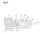
- the ceramic resistor 10 is configured in the following manner.
- the first resistor portion 11 assumes the shape resembling the letter U, and a bottom portion of the U shape is positioned in the vicinity of the front end of the heater body 2.
- the second resistor portions 12 assume a rodlike shape and extend rearward along the direction of the axis O substantially in parallel with each other from the corresponding end portions of the U-shaped first resistor portion 11.
- the first resistor portion 11 is configured such that the front end part 11a has a diameter smaller than that of the opposite end parts 11b.
- a joint interface 15 between the first resistor portion 11 and each of the second resistor portions 12 is formed at each of the opposite end parts 11b, whose diameter is greater than that of the front end part 11a.
- the area of a cross section taken perpendicularly to the axis of each of the second resistor portions 12 is set greater than the cross-sectional area of the front end part 11a of the first resistor portion (herein the cross-sectional area is defined as the area of a cross section taken along a plane perpendicularly intersecting a reference plane K, which will be described later). That is, the U-shaped ceramic resistor 10 is configured in the following manner. Two large-diameter rodlike portions Ld, whose diameter is greater than that of the U-shaped front end part 11a of the ceramic resistor 10, are connected to the corresponding ends of the front end part 11a and serve as electricity conduction paths to the front end part 11a. The joint interfaces 15 between the first resistor portion 11 and the second resistor portions 12 are formed at the corresponding large-diameter portions Ld.
- the joint interfaces 15 are those of ceramic resistors formed of different materials. Accordingly, in an application involving frequent repetition of temperature rise and cooling as in the case of a glow plug, thermal stress induced by the difference in coefficient of linear expansion between the two ceramics tends to concentrate at the joint interface 15.
- formation of the joint interfaces 15 at the respective large-diameter rodlike portions Ld the area of joint can be increased, and thus the margin for strength against thermal stress concentration can be increased, whereby a ceramic heater having excellent durability can be realized.
- Positioning of the joint interface 15 at the large-diameter rodlike portion Ld means that at least the joint interface 15 is not formed at the small-diameter front end part 11a.
- the distance between the joint interface 15 and the front end position of the ceramic resistor 10, where temperature rises to the highest level by heat generation, can be increased accordingly, thereby restraining the joint interface 15 from subjection to an excessively great temperature gradient and heating-cooling cycles of great temperature hysteresis.
- the joint interface 15 of the present embodiment further has the following two features.
- a joint portion of the ceramic resistor 10 between the first resistor portion 11 and the second resistor portion 12 is adjusted in S/S0 to not less than 1.2 and not greater than 10, where S represents the total area of the joint interface 15, and S0 represents the area of a cross section whose area is the smallest among those of cross sections perpendicularly intersecting the axis O of the heater body 2 at arbitrary positions.
- S/S0 value is not greater than 1.2, the effect of expanding the joint interface 15 is poor.
- the joint portion becomes long, resulting in an unnecessary increase in the dimension of the ceramic heater 1.
- the joint interface 15 may be entirely formed of an inclined face portion.
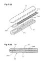
- a preliminary green body which is to be used as an insert is formed such that the end face thereof which is to become the joint interface 15 includes sharp end portions as represented by the dashed line in Fig. 3(a); as a result, chipping or a like problem becomes likely to occur.
- the end portions of the joint interface may each assume the form of a gently inclined face 15e or a face perpendicularly intersecting the axis J of the second resistor portion 12.
- ⁇ represents the crossing angle between an outline of the ceramic resistor 10 and a line representing the joint interface 15, a ⁇ value as measured on a section taken along a plane (in Fig. 4, the plane is the reference plane K) which minimizes ⁇ is not less than 20°.
- Employment of such a ⁇ value prevents occurrence of chipping or a like problem on the above-mentioned green body.
- ⁇ assumes a maximum value of 90°.
- the inclined face portion 15t preferably assumes a planar shape as shown in Fig. 4. However, so long as the effect of an inclined face portion is not impaired, the inclined face portion 15t may be curved at a slight radius of curvature as represented by the dash-and-dot line in Fig. 4, whereby the area of joint can be further increased.
- a pair of second resistor portions 12 of the ceramic resistor 10 are exposed, from the surface of the heater body 2, at axially rear end parts thereof to thereby form respective exposed parts 12a, and the exposed parts 12 serve as joint regions where electricity-conduction terminal elements 16 and 17 are joined to the ceramic resistor 10.
- This structure does not require embedment of electricity conduction lead wires in the heater body 2 and allows the heater body 2 to be formed of all-ceramic, thereby reducing the number of manufacturing steps.
- the ceramic substrate 13 is partially cut off at a rear end portion thereof as viewed along the direction of the axis O of the heater body 2 to thereby form a cut portion 13a, where the rear end parts of the second resistor portions 12 are exposed.
- a cut portion 13a may be formed at the stage of a green body or may be formed by grinding or a like process after firing.
- the electricity-conduction terminal elements 16 and 17 are made of metal, such as Ni or an Ni alloy, and are brazed to the corresponding second resistor portions 12 at the exposed parts 12a. Since metal and ceramic are to be brazed, preferably, an active brazing filler metal suited for such brazing is used; alternatively, an active metal component is deposed on ceramic for metallization by vapor deposition or a like process, and subsequently brazing is performed by use of an ordinary brazing filler metal.
- An applicable brazing filler metal can be of a known Ag type or Cu type, and an applicable active metal component is one or more elements selected from the group consisting of Ti, Zr, and Hf.
- a metallic rod 6 for supplying electricity to the ceramic heater 1 is inserted into the metallic shell 4 from a rear end thereof as viewed along the direction of the axis O and is disposed therein while being electrically insulated therefrom.
- a ceramic rig 31 is disposed between the outer circumferential surface of a rear portion of the metallic rod 6 and the inner circumferential surface of the metallic shell 4, and a glass filler layer 32 is formed on the rear side of the ceramic ring 31 to thereby fix the metallic rod 6 in place.
- a ring-side engagement portion 31a which assumes the form of a large-diameter portion, is formed on the outer circumferential surface of the ceramic ring 31.
- a shell-side engagement portion 4e which assumes the form of a circumferentially extending stepped portion, is formed on the inner circumferential surface of the metallic shell 4 at a position biased toward the rear end of the metallic shell 4.
- the ring-side engagement portion 31a is engaged with the shell-side engagement portion 4e, to thereby prevent the ceramic ring 31 from slipping axially forward.
- An outer circumferential surface of the metallic rod 6 in contact with the glass filler layer 32 is knurled by knurling or a like process (in Fig. 1, the hatched region).
- a rear end portion of the metallic rod 6 projects rearward from the metallic shell 4, and a metallic terminal member 7 is fitted to the projecting portion via an insulating bushing 8.
- the metallic terminal member 7 is fixedly attached to the outer circumferential surface of the metallic rod 6 in an electrically continuous condition by a circumferentially crimped portion 9.
- one second resistor portion 12 is joined at the exposed part 12a thereof to the grounding electricity-conduction terminal element 16 to thereby be electrically connected to the metallic shell 4 via the metallic sleeve 3, whereas the other second resistor portion 12 is joined at the exposed part 12a thereof to the power-supply-side electricity-conduction terminal element 17 to thereby be electrically connected to the metallic rod 6.
- the exposed part 12a of the second resistor portion 12 is formed at a rear end portion of the outer circumferential surface of the heater body 2, and the heater body 2 is disposed such that a rear end face 2r thereof is located frontward from a rear end face 3r of the metallic sleeve 3 as viewed along the direction of the axis O.
- the grounding metallic lead element 16 is disposed in such a manner as to connect the exposed part 12a of the heater body 2 and a rear end portion of the inner circumferential surface of the metallic sleeve 3. A portion of the metallic sleeve 3 which is located rearward from the front end edge of the cut portion 13a of the heater body 2, which will be described later, is filled with glass 30. As a result, the grounding electricity-conduction terminal element 16 is substantially entirely embedded in the glass 30 and is thus unlikely to suffer breaking, defective contact, or a like problem even when vibration or a like disturbance is imposed thereon. In the present embodiment, the grounding electricity-conduction terminal element 16 is a strap-like metallic member.
- a front end portion of one side 16a of the grounding electricity-conduction terminal element 16 is brazed to the corresponding second resistor portion 12, whereas a rear end portion of an opposite side 16b is joined to a rear end portion of the inner circumferential surface of the metallic sleeve 3 by, for example, brazing or spot welding.
- the grounding electricity-conduction terminal element 16 can be easily joined.
- the inclined face portion 15t of the joint interface 15 of the ceramic resistor 10 is formed perpendicular to the aforementioned reference plane K (in parallel with the paper on which Fig. 4 appears).
- the inclined face portion 15t can be inclined in either of the following two directions: as shown in Fig. 9, the first resistor portion 11 and the second resistor portion 12 are in contact with each other at the inclined face portion 15t such that the first resistor portion 11 is disposed on the outer side of the second resistor portion 12 in the radial direction R with respect to the axis O of the heater body 2; and as shown in Fig. 10, the second resistor portion 12 is disposed on the outer side of the first resistor portion 11 in the radial direction R.
- a resistor green body 34 (Fig. 6), which is to become the ceramic resistor 10, is formed by injection molding; specifically, insert molding.
- Fig. 5 shows an example of a molding process. Molding uses a split mold having an injection cavity for molding the resistor green body 34.
- the split mold is composed of a first mold 50A or 50B and a second mold 51.
- the injection cavity is divided into a cavity formed in the first mold 50A or 50B and a cavity formed in the second mold 51, along a dividing plane DP corresponding to the reference plane K.
- the second mold 51 has a second integral injection cavity 57 formed therein.
- the second integral injection cavity 57 is integrally composed of a cavity 55 for molding the first resistor portion 11 (Fig. 2) and a cavity 56 for molding the second resistor portions 12 (Fig. 2).
- a preliminary-molding mold 50A and an insert-molding mold 50B are prepared to serve as the first mold.
- the preliminary-molding mold 50A has a partial injection cavity 58 formed therein for molding preliminary green bodies 34b, which is to become the second resistor portions 12.
- the preliminary-molding mold 50A includes a filler portion 60 for filling, when mated with the second mold 51, a portion 55 of the second integral injection cavity 57 which is not used for molding the preliminary green bodies 34b.
- the filler portion 60 has an adjacent face 59 adjacent to the partial injection cavity 58 and perpendicular to the dividing plane DP.
- the insert-molding mold 50B has a first integral injection cavity 63 formed therein.
- the first integral injection cavity 63 is integrally composed of a cavity 61 for molding the first resistor portion 11 (Fig. 2) and a cavity 62 for molding the second resistor portions 12 (Fig. 2).
- the second mold 51 and the preliminary-molding mold 50A are mated with each other, and a molding compound CP1 is injected to thereby mold the preliminary green bodies 34b.
- the molding compound CP1 is prepared by the steps of mixing a tungsten carbide powder, a silicon nitride powder, and a sintering aid powder so as to obtain the composition of the second electrically conductive ceramic, thereby yielding a material ceramic powder; kneading a mixture of the material ceramic powder and an organic binder to obtain a compound; and fluidizing the compound through application of heat.
- the split mold Upon completion of injection molding of the preliminary green bodies 34b, the split mold is opened. Since the joint interface 15 between the first resistor portion 11 and the second resistor portion 12 is only formed of planes perpendicular to the reference plane K; i.e., the dividing plane DP, the split mold can be readily opened without inflicting damage to the preliminary green bodies 34b, by separating the preliminary-molding mold 50A from the second mold 51 in the direction perpendicular to the dividing plane DP.
- the second mold 51 and the insert-molding mold 50B are mated with each other while the preliminary green bodies 34b are disposed as inserts in the corresponding cavity portions 56 and 62 of the first integral injection cavity 63 and the second integral injection cavity 57.
- a molding compound CP2 is injected into the remaining cavity portions 55 and 61 to thereby yield the resistor green body 34 through integration of an injection-molded portion 34a (Fig. 6) with the preliminary green bodies 34b.
- the molding compound CP2 is similar to the molding compound CP1; however, a material powder for the molding compound CP2 is blended so as to obtain the composition of the first electrically conductive ceramic.
- the preliminary-molding mold 50A is replaced with the insert-molding mold 50B, followed by insert molding, whereby working efficiency is further enhanced.
- the molding sequence of the first resistor portion 11 and the second resistor portions 12 can be reversed.
- a preliminary-molding mold must include a filler portion which fills the cavity portion 56 of the second integral injection cavity 57.
- the first resistor portion 11 is smaller in dimension as measured along the direction of the axis O of the heater body 2 than the second resistor portion 12.
- the preliminary green bodies 34b correspond to the second resistor portions 12, thereby yielding the following advantage.
- forming sprues SP1 for injecting a compound therethrough at a longitudinally rear end portion of the cavity is favorable for uniform injection of the molding compound CP1 into the cavity.
- the moving distance of the fluidized molding compound CP1 becomes considerably long.
- the temperature of a molten binder unavoidably drops to a certain extent.
- the moving distance of the fluidized molding compound CP2 is short, and therefore temperature drop becomes unlikely.
- the insert molding process of the present embodiment allows the molding compound CP2 to reach the joint interface at higher temperature, thereby providing a strong joint with few defects.
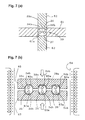
- a material powder for forming the ceramic substrate 13 is die-pressed beforehand into half green bodies 36 and 37, which are upper and lower substrate green bodies formed separately, as shown in Fig. 6(a).
- a recess 37a (a recess formed on the half green body 36 is unseen on Fig. 6(a)) having a shape corresponding to the resistor green body 34 is formed on the mating surface of each of the half green bodies 36 and 37.
- the half green bodies 36 and 37 are joined together at the above-mentioned mating surfaces, while the resistor green body 34 is accommodated in the recesses 37a. Then, as shown in Fig.
- the thus-obtained composite green body 39 is calcined at a predetermined temperature (e.g., approximately 600°C) to thereby become a calcined body 39' (notably, a calcined body is considered a composite green body in the broad sense) shown in Fig. 6(b).
- a predetermined temperature e.g., approximately 600°C
- the calcined body 39' is placed in cavities 65a of hot-pressing dies 65 made of graphite or a like material.
- the calcined body 39' held between the pressing dies 65 is placed in a kiln 64.
- the calcined body 39' is sintered at a predetermined firing retention temperature (not lower than 1700°C; e.g., about 1800°C) in a predetermined atmosphere while being pressed between the pressing dies 65, to thereby become a sintered body 70 as shown in Fig. 8(c).
- the calcined body 39' shown in Fig. 7(b) is fired while being compressed in the direction along the mating surface 39a of the half green bodies 36 and 37, to thereby become the sintered body 70 as shown in Fig. 8(c).
- the green bodies (preliminary green bodies) 34b, which is to become the second resistor portions, of the resistor green body 34 are deformed such that the circular cross sections thereof are squeezed along the above-mentioned direction of compression; i.e., along the direction along which the axes J approach each other, to thereby become the second resistor portions 12 each having an elliptic cross section.
- the external surface of the thus-obtained sintered body 70 of Fig. 8(c) is, for example, polished such that the cross section of the ceramic substrate 13 assumes a circular shape as shown in Fig. 8(d), thereby yielding the final heater body 2 (ceramic heater 1).
- Necessary components, such as the metallic sleeve 3, the electricity-conduction terminal elements 16 and 17, and the metallic shell 4, are attached to the ceramic heater 1, thereby completing the glow plug 50 shown in Fig. 1.
- the ceramic heater 1 to be used in the glow plug 50 shown in Figs. 1 and 2 is configured such that the joint interface 15 of the ceramic resistor 10 is merely formed of the planes 15t and 15e perpendicularly intersecting the reference plane K (achievement of the first object) and such that a portion of the joint face 15 assumes the form of the inclined face portion 15t (achievement of the second object).
- the joint interface 15 can include the inclined face portion 15t which is inclined with respect to the reference plane K.
- a plane on which the aforementioned crossing angle 0 is determined can be defined as a plane K' including the axis J and perpendicularly intersecting the reference plane K.
- a ceramic heater can be configured in such a manner as to merely fulfill the requirements for achievement of the first object only.
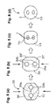
- a groove 15a perpendicularly intersecting the reference plane K is formed on either the first resistor portion 11 or the second resistor portions 12 (on the second resistor portions 12 in the present embodiment), whereas a protrusion 15b, which perpendicularly intersects the reference plane K and is engaged with the groove 15a, is formed on the other (on the first resistor portion 11 in the present embodiment).
- Fig. 3(c) is a perspective view schematically showing the joint interface 15 on the second resistor portion 12 (on which the groove 15a is formed).
- Fig. 3(b) is a perspective view showing the joint interface 15 on the second resistor portion 12.
- plane portions 15d for dulling the crossing angle ⁇ are formed at the corresponding opposite end portions of the curved surface 15c.
- the ceramic heaters shown in Figs. 13 and 14 can be considered as being configured in the following manner.
- the direction in parallel with the reference plane K (see Fig. 3) and perpendicular to the axis O (in Fig. 3, the axis J may serve as the axis O) is defined as the width direction W.
- the joint interface 15 between the first resistor portion 11 and each of the second resistor portions 12 is shaped such that a portion 15c located at a middle position along the width direction W projects beyond the residual portion into the side toward the first resistor portion 11 (Fig. 14) or the side toward the second resistor portion 12 (Fig. 13). The thus-shaped joint interface 15 further enhances the joined state between the first resistor portion 11 and the second resistor portion 12.
- the joint interface 15 is shaped such that the portion 15c located at a middle position along the width direction W projects beyond the residual portion into the side toward the second resistor portion 12.
- a prospective joint interface 115 of the preliminary green body 34b with the injection-molded portion 34a has a recess 115c formed therein at a middle position along the width direction.
- the molding compound CP2 is filled into the recess 115c to thereby integrate the injection-molded portion 34a with the preliminary green body 34b.
- This process is similar to that which has been described previously with reference to Fig. 5, except that the prospective joint interface 115 is employed in place of the adjacent face 59.
- the molding compound CP2 comes into contact with end regions 115p located at opposite end portions of the recess 115c of the prospective joint interface 115 and is then filled into the interior of the recess 115c.
- a portion of the molten molding compound CP2 which is filled into the interior of the recess 115c tends to drop in temperature than a portion which comes into contact with the end regions 115p.
- a defective portion which exhibits incomplete joint to the preliminary green body 34b may be formed within the recess 115c.
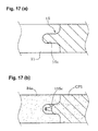
- Fig. 18(a) shows an example in which the portion 15c of the joint interface 15 located at a middle position along the width direction W projects beyond the residual portion into the side toward the first resistor portion 11.
- the resistor green body 34 is formed in such a manner as to include the preliminary green body 34a corresponding to the first resistor portion 11. Therefore, as shown in Fig. 17(b), in the course of integrating the preliminary green body 34a with the injection-molded portions corresponding to the second resistor portions 12 through insert molding, the recess 115c formed in the preliminary green body 34a is filled with the molding compound CP1.
- Fig. 18 shows an example of a specific manufacturing process for manufacturing the resistor green body 34.
- a preliminary-molding mold 50C includes a filler portion 161 for filling, when mated with the second mold 51, a portion 56 of the second integral injection cavity 57 which is not used for molding the preliminary green body 34a.
- the adjacent face 59 assumes a shape corresponding to the joint interface 15 shown in Fig. 17(b).
- the insert-molding mold 50B is similar to that of Fig. 5.
- the second mold 51 and the preliminary-molding mold 50C are mated with each other, and the molding compound CP2 is injected to thereby mold the preliminary green body 34a.
- the second mold 51 and the insert-molding mold 50B are mated with each other while the preliminary green body 34a is disposed as an insert in the cavity portions 55 and 61 of the first integral injection cavity 63 and the second integral injection cavity 57.
- the molding compound CP1 is injected into the remaining cavity portions 56 and 62 to thereby yield the resistor green body 34 through integration of the injection-molded portions 34b with the preliminary green 34a.
Landscapes
- Engineering & Computer Science (AREA)
- Chemical & Material Sciences (AREA)
- Combustion & Propulsion (AREA)
- Mechanical Engineering (AREA)
- General Engineering & Computer Science (AREA)
- Ceramic Engineering (AREA)
- Resistance Heating (AREA)
Applications Claiming Priority (2)
| Application Number | Priority Date | Filing Date | Title |
|---|---|---|---|
| JP2001135621 | 2001-05-02 | ||
| JP2001135621 | 2001-05-02 |
Publications (3)
| Publication Number | Publication Date |
|---|---|
| EP1255076A2 true EP1255076A2 (fr) | 2002-11-06 |
| EP1255076A3 EP1255076A3 (fr) | 2006-10-25 |
| EP1255076B1 EP1255076B1 (fr) | 2009-02-18 |
Family
ID=18983050
Family Applications (1)
| Application Number | Title | Priority Date | Filing Date |
|---|---|---|---|
| EP02253074A Expired - Lifetime EP1255076B1 (fr) | 2001-05-02 | 2002-05-01 | Elément chauffant céramique, bougie à incandescence comportant cet élément chauffant et procédé de fabrication |
Country Status (3)
| Country | Link |
|---|---|
| US (1) | US6653601B2 (fr) |
| EP (1) | EP1255076B1 (fr) |
| DE (1) | DE60231164D1 (fr) |
Cited By (6)
| Publication number | Priority date | Publication date | Assignee | Title |
|---|---|---|---|---|
| US20100288747A1 (en) * | 2007-10-29 | 2010-11-18 | Kyocera Corporation | Ceramic heater and glow plug provided therewith |
| US20110114622A1 (en) * | 2008-02-20 | 2011-05-19 | Ngk Spark Plug Co., Ltd. | Ceramic heater and glow plug |
| JP2013164230A (ja) * | 2012-02-13 | 2013-08-22 | Ngk Spark Plug Co Ltd | グロープラグの製造方法 |
| CN103493586A (zh) * | 2011-04-27 | 2014-01-01 | 京瓷株式会社 | 加热器以及具有该加热器的电热塞 |
| EP2667686A4 (fr) * | 2011-01-20 | 2017-06-21 | Kyocera Corporation | Réchauffeur et bougie de préchauffage munie de celui-ci |
| CN112335334A (zh) * | 2018-09-11 | 2021-02-05 | 京瓷株式会社 | 加热器以及具备该加热器的香烟用加热用具 |
Families Citing this family (16)
| Publication number | Priority date | Publication date | Assignee | Title |
|---|---|---|---|---|
| JP3886449B2 (ja) * | 2002-12-26 | 2007-02-28 | 日本特殊陶業株式会社 | グロープラグ及びグロープラグの取付け構造 |
| US7351935B2 (en) * | 2004-06-25 | 2008-04-01 | Ngk Spark Plug Co., Ltd. | Method for producing a ceramic heater, ceramic heater produced by the production method, and glow plug comprising the ceramic heater |
| EP1612486B1 (fr) * | 2004-06-29 | 2015-05-20 | Ngk Spark Plug Co., Ltd | Bougie à incandesence |
| US7696455B2 (en) * | 2006-05-03 | 2010-04-13 | Watlow Electric Manufacturing Company | Power terminals for ceramic heater and method of making the same |
| EP2117280B1 (fr) * | 2007-02-22 | 2018-04-11 | Kyocera Corporation | Dispositif de chauffage en ceramique, bougie de prechauffage utilisant le dispositif de chauffage en ceramique, et procede de fabrication du dispositif de chauffage en ceramique |
| CN101874182A (zh) * | 2007-09-23 | 2010-10-27 | 圣戈本陶瓷及塑料股份有限公司 | 加热元件系统 |
| US20100078421A1 (en) * | 2008-10-01 | 2010-04-01 | Federal-Mogul Italy Sr1 | Glow plug adn heater assembly therefor with an improved connection between a central electrode and a heater probe of the heater assembly |
| JP5279447B2 (ja) * | 2008-10-28 | 2013-09-04 | 京セラ株式会社 | セラミックヒータ |
| EP2496051B1 (fr) * | 2009-10-27 | 2017-01-04 | Kyocera Corporation | Réchauffeur en céramique |
| EP2600688B1 (fr) | 2010-07-30 | 2019-06-19 | Kyocera Corporation | Élément chauffant et sa bougie de préchauffage |
| EP2753144B1 (fr) * | 2011-08-29 | 2019-07-17 | Kyocera Corporation | Élément chauffant et bougie à incandescence équipée de celui-ci |
| JP6140955B2 (ja) * | 2011-12-21 | 2017-06-07 | 日本特殊陶業株式会社 | セラミックヒータの製造方法 |
| DE102012205081B4 (de) | 2012-03-29 | 2024-07-18 | Robert Bosch Gmbh | Verfahren zur Herstellung einer keramischen Mehrkomponenten-Glühstiftkerze und dazugehöriges Werkzeug |
| JP6246063B2 (ja) * | 2014-05-02 | 2017-12-13 | 日本特殊陶業株式会社 | スパークプラグ |
| DE102016114929B4 (de) * | 2016-08-11 | 2018-05-09 | Borgwarner Ludwigsburg Gmbh | Druckmessglühkerze |
| DE102016121346B4 (de) * | 2016-10-27 | 2018-05-09 | Borgwarner Ludwigsburg Gmbh | Glühkerze |
Citations (1)
| Publication number | Priority date | Publication date | Assignee | Title |
|---|---|---|---|---|
| JPH0344632A (ja) | 1989-07-12 | 1991-02-26 | Mitsubishi Paper Mills Ltd | 写真用支持体の製造方法 |
Family Cites Families (10)
| Publication number | Priority date | Publication date | Assignee | Title |
|---|---|---|---|---|
| JP3044632B2 (ja) | 1991-02-20 | 2000-05-22 | ボッシュ ブレーキ システム株式会社 | セラミックヒータ型グロープラグ |
| US5750958A (en) * | 1993-09-20 | 1998-05-12 | Kyocera Corporation | Ceramic glow plug |
| JP3625627B2 (ja) * | 1996-10-14 | 2005-03-02 | 日本特殊陶業株式会社 | 高温下で使用されるセラミック応用電子機器及びその製造方法 |
| JP3839174B2 (ja) * | 1998-01-30 | 2006-11-01 | 日本特殊陶業株式会社 | セラミックヒータの製造方法 |
| JPH11257659A (ja) * | 1998-03-10 | 1999-09-21 | Ngk Spark Plug Co Ltd | セラミックヒータ及びセラミックグロープラグ |
| JP3908864B2 (ja) * | 1998-09-11 | 2007-04-25 | 日本特殊陶業株式会社 | セラミックヒータ |
| JP3865953B2 (ja) * | 1998-10-26 | 2007-01-10 | 日本特殊陶業株式会社 | セラミックグロープラグ |
| US6423944B2 (en) * | 2000-01-25 | 2002-07-23 | Ngk Spark Plug Co., Ltd. | Ceramic heater and glow plug with reference zone and condensed zone of ceramics and conductive particles dispersed therein |
| JP4169929B2 (ja) * | 2000-12-22 | 2008-10-22 | 日本特殊陶業株式会社 | グロープラグ |
| JP4808852B2 (ja) * | 2001-01-17 | 2011-11-02 | 日本特殊陶業株式会社 | 窒化珪素/炭化タングステン複合焼結体 |
-
2002
- 2002-05-01 EP EP02253074A patent/EP1255076B1/fr not_active Expired - Lifetime
- 2002-05-01 US US10/135,770 patent/US6653601B2/en not_active Expired - Lifetime
- 2002-05-01 DE DE60231164T patent/DE60231164D1/de not_active Expired - Lifetime
Patent Citations (1)
| Publication number | Priority date | Publication date | Assignee | Title |
|---|---|---|---|---|
| JPH0344632A (ja) | 1989-07-12 | 1991-02-26 | Mitsubishi Paper Mills Ltd | 写真用支持体の製造方法 |
Cited By (13)
| Publication number | Priority date | Publication date | Assignee | Title |
|---|---|---|---|---|
| US20100288747A1 (en) * | 2007-10-29 | 2010-11-18 | Kyocera Corporation | Ceramic heater and glow plug provided therewith |
| US20110114622A1 (en) * | 2008-02-20 | 2011-05-19 | Ngk Spark Plug Co., Ltd. | Ceramic heater and glow plug |
| US8378273B2 (en) * | 2008-02-20 | 2013-02-19 | Ngk Spark Plug Co., Ltd. | Ceramic heater and glow plug |
| EP2667686A4 (fr) * | 2011-01-20 | 2017-06-21 | Kyocera Corporation | Réchauffeur et bougie de préchauffage munie de celui-ci |
| EP2704519A4 (fr) * | 2011-04-27 | 2014-10-01 | Kyocera Corp | Élément chauffant et bougie incandescente comprenant ledit élément |
| EP2704519A1 (fr) | 2011-04-27 | 2014-03-05 | Kyocera Corporation | Élément chauffant et bougie incandescente comprenant ledit élément |
| CN103493586A (zh) * | 2011-04-27 | 2014-01-01 | 京瓷株式会社 | 加热器以及具有该加热器的电热塞 |
| CN103493586B (zh) * | 2011-04-27 | 2015-11-25 | 京瓷株式会社 | 加热器以及具有该加热器的电热塞 |
| US9491805B2 (en) | 2011-04-27 | 2016-11-08 | Kyocera Corporation | Heater and glow plug provided with same |
| US10299317B2 (en) | 2011-04-27 | 2019-05-21 | Kyocera Corporation | Heater and glow plug provided with same |
| JP2013164230A (ja) * | 2012-02-13 | 2013-08-22 | Ngk Spark Plug Co Ltd | グロープラグの製造方法 |
| CN112335334A (zh) * | 2018-09-11 | 2021-02-05 | 京瓷株式会社 | 加热器以及具备该加热器的香烟用加热用具 |
| CN112335334B (zh) * | 2018-09-11 | 2022-12-09 | 京瓷株式会社 | 加热器以及具备该加热器的加热用具 |
Also Published As
| Publication number | Publication date |
|---|---|
| US20020162831A1 (en) | 2002-11-07 |
| US6653601B2 (en) | 2003-11-25 |
| EP1255076B1 (fr) | 2009-02-18 |
| DE60231164D1 (de) | 2009-04-02 |
| EP1255076A3 (fr) | 2006-10-25 |
Similar Documents
| Publication | Publication Date | Title |
|---|---|---|
| EP1255075B1 (fr) | Elément chauffant céramique, et bougie à incandescence comportant cet élément | |
| EP1255076B1 (fr) | Elément chauffant céramique, bougie à incandescence comportant cet élément chauffant et procédé de fabrication | |
| JP3924193B2 (ja) | セラミックヒータ、それを用いたグロープラグ及びセラミックヒータの製造方法 | |
| EP1443273B1 (fr) | Bougie à incandescence et sa méthode de fabrication | |
| EP1768456B1 (fr) | Radiateur céramique, et connecteur néon utilisant ledit radiateur | |
| JP4751392B2 (ja) | ロウ付け構造体、セラミックヒータおよびグロープラグ | |
| JP4348317B2 (ja) | グロープラグ | |
| KR100399114B1 (ko) | 세라믹히터 | |
| JP2005315447A (ja) | セラミックヒーターおよびグロープラグ | |
| JP2006024394A (ja) | セラミックヒータおよびグロープラグ | |
| JP4546756B2 (ja) | セラミックヒータおよびグロープラグ | |
| JP4562315B2 (ja) | セラミックヒータ、セラミックヒータの製造方法及びグロープラグ | |
| JP3269253B2 (ja) | セラミックヒータ | |
| JP2001052845A (ja) | セラミックヒータ | |
| JP2000218671A (ja) | 射出成形用ノズル | |
| JP4560249B2 (ja) | グロープラグ | |
| JP2006351446A (ja) | セラミックヒータの製造方法及びグロープラグ | |
| JP2002364841A (ja) | グロープラグ | |
| JP2002289327A (ja) | セラミックヒータ及びそれを備えるグロープラグ | |
| JP3115254B2 (ja) | セラミックヒータ | |
| JP3160226B2 (ja) | セラミックヒータ | |
| JP2002333136A (ja) | グロープラグ | |
| JP2002124363A (ja) | セラミックヒータ | |
| JP2001068257A (ja) | セラミックヒータ | |
| JP2001132947A (ja) | セラミックヒータ及びそれを備えるグロープラグ |
Legal Events
| Date | Code | Title | Description |
|---|---|---|---|
| PUAI | Public reference made under article 153(3) epc to a published international application that has entered the european phase |
Free format text: ORIGINAL CODE: 0009012 |
|
| AK | Designated contracting states |
Kind code of ref document: A2 Designated state(s): AT BE CH CY DE DK ES FI FR GB GR IE IT LI LU MC NL PT SE TR |
|
| AX | Request for extension of the european patent |
Free format text: AL;LT;LV;MK;RO;SI |
|
| PUAL | Search report despatched |
Free format text: ORIGINAL CODE: 0009013 |
|
| AK | Designated contracting states |
Kind code of ref document: A3 Designated state(s): AT BE CH CY DE DK ES FI FR GB GR IE IT LI LU MC NL PT SE TR |
|
| AX | Request for extension of the european patent |
Extension state: AL LT LV MK RO SI |
|
| 17P | Request for examination filed |
Effective date: 20070418 |
|
| AKX | Designation fees paid |
Designated state(s): DE FR GB IT |
|
| 17Q | First examination report despatched |
Effective date: 20070620 |
|
| GRAP | Despatch of communication of intention to grant a patent |
Free format text: ORIGINAL CODE: EPIDOSNIGR1 |
|
| GRAS | Grant fee paid |
Free format text: ORIGINAL CODE: EPIDOSNIGR3 |
|
| GRAS | Grant fee paid |
Free format text: ORIGINAL CODE: EPIDOSNIGR3 |
|
| GRAA | (expected) grant |
Free format text: ORIGINAL CODE: 0009210 |
|
| AK | Designated contracting states |
Kind code of ref document: B1 Designated state(s): DE FR GB IT |
|
| REG | Reference to a national code |
Ref country code: GB Ref legal event code: FG4D |
|
| REF | Corresponds to: |
Ref document number: 60231164 Country of ref document: DE Date of ref document: 20090402 Kind code of ref document: P |
|
| PLBE | No opposition filed within time limit |
Free format text: ORIGINAL CODE: 0009261 |
|
| STAA | Information on the status of an ep patent application or granted ep patent |
Free format text: STATUS: NO OPPOSITION FILED WITHIN TIME LIMIT |
|
| 26N | No opposition filed |
Effective date: 20091119 |
|
| GBPC | Gb: european patent ceased through non-payment of renewal fee |
Effective date: 20090518 |
|
| PG25 | Lapsed in a contracting state [announced via postgrant information from national office to epo] |
Ref country code: GB Free format text: LAPSE BECAUSE OF NON-PAYMENT OF DUE FEES Effective date: 20090518 |
|
| PG25 | Lapsed in a contracting state [announced via postgrant information from national office to epo] |
Ref country code: IT Free format text: LAPSE BECAUSE OF FAILURE TO SUBMIT A TRANSLATION OF THE DESCRIPTION OR TO PAY THE FEE WITHIN THE PRESCRIBED TIME-LIMIT Effective date: 20090218 |
|
| REG | Reference to a national code |
Ref country code: FR Ref legal event code: PLFP Year of fee payment: 15 |
|
| REG | Reference to a national code |
Ref country code: FR Ref legal event code: PLFP Year of fee payment: 16 |
|
| REG | Reference to a national code |
Ref country code: FR Ref legal event code: PLFP Year of fee payment: 17 |
|
| PGFP | Annual fee paid to national office [announced via postgrant information from national office to epo] |
Ref country code: FR Payment date: 20190327 Year of fee payment: 18 |
|
| PG25 | Lapsed in a contracting state [announced via postgrant information from national office to epo] |
Ref country code: FR Free format text: LAPSE BECAUSE OF NON-PAYMENT OF DUE FEES Effective date: 20200531 |
|
| PGFP | Annual fee paid to national office [announced via postgrant information from national office to epo] |
Ref country code: DE Payment date: 20210408 Year of fee payment: 20 |
|
| REG | Reference to a national code |
Ref country code: DE Ref legal event code: R071 Ref document number: 60231164 Country of ref document: DE |