EP1255301B1 - Dispositiv de protection contre les décharges électrostatiques à layout configurable pour circuits integrés - Google Patents
Dispositiv de protection contre les décharges électrostatiques à layout configurable pour circuits integrés Download PDFInfo
- Publication number
- EP1255301B1 EP1255301B1 EP02290153A EP02290153A EP1255301B1 EP 1255301 B1 EP1255301 B1 EP 1255301B1 EP 02290153 A EP02290153 A EP 02290153A EP 02290153 A EP02290153 A EP 02290153A EP 1255301 B1 EP1255301 B1 EP 1255301B1
- Authority
- EP
- European Patent Office
- Prior art keywords
- doped region
- highly
- weakly
- lateral
- region
- Prior art date
- Legal status (The legal status is an assumption and is not a legal conclusion. Google has not performed a legal analysis and makes no representation as to the accuracy of the status listed.)
- Expired - Lifetime
Links
- 230000004224 protection Effects 0.000 claims description 15
- 238000000034 method Methods 0.000 description 21
- 230000008569 process Effects 0.000 description 21
- 238000005516 engineering process Methods 0.000 description 11
- 230000015556 catabolic process Effects 0.000 description 8
- 230000008859 change Effects 0.000 description 8
- 230000000694 effects Effects 0.000 description 7
- 239000000758 substrate Substances 0.000 description 6
- 230000008901 benefit Effects 0.000 description 5
- 230000001960 triggered effect Effects 0.000 description 5
- 239000002019 doping agent Substances 0.000 description 4
- 230000009467 reduction Effects 0.000 description 4
- 238000009792 diffusion process Methods 0.000 description 3
- 230000006870 function Effects 0.000 description 3
- 239000007943 implant Substances 0.000 description 3
- 238000005259 measurement Methods 0.000 description 3
- 238000012360 testing method Methods 0.000 description 3
- 230000007423 decrease Effects 0.000 description 2
- 238000013461 design Methods 0.000 description 2
- 230000008713 feedback mechanism Effects 0.000 description 2
- 238000002513 implantation Methods 0.000 description 2
- 238000000059 patterning Methods 0.000 description 2
- 238000000926 separation method Methods 0.000 description 2
- 230000007704 transition Effects 0.000 description 2
- 101100207343 Antirrhinum majus 1e20 gene Proteins 0.000 description 1
- 230000005540 biological transmission Effects 0.000 description 1
- 239000002800 charge carrier Substances 0.000 description 1
- 230000003247 decreasing effect Effects 0.000 description 1
- 230000001419 dependent effect Effects 0.000 description 1
- 238000001514 detection method Methods 0.000 description 1
- 230000002542 deteriorative effect Effects 0.000 description 1
- 230000005684 electric field Effects 0.000 description 1
- 238000002474 experimental method Methods 0.000 description 1
- 230000003116 impacting effect Effects 0.000 description 1
- 239000012535 impurity Substances 0.000 description 1
- 230000003071 parasitic effect Effects 0.000 description 1
- 230000003068 static effect Effects 0.000 description 1
Images


Classifications
-
- H—ELECTRICITY
- H10—SEMICONDUCTOR DEVICES; ELECTRIC SOLID-STATE DEVICES NOT OTHERWISE PROVIDED FOR
- H10D—INORGANIC ELECTRIC SEMICONDUCTOR DEVICES
- H10D89/00—Aspects of integrated devices not covered by groups H10D84/00 - H10D88/00
- H10D89/60—Integrated devices comprising arrangements for electrical or thermal protection, e.g. protection circuits against electrostatic discharge [ESD]
- H10D89/601—Integrated devices comprising arrangements for electrical or thermal protection, e.g. protection circuits against electrostatic discharge [ESD] for devices having insulated gate electrodes, e.g. for IGFETs or IGBTs
- H10D89/711—Integrated devices comprising arrangements for electrical or thermal protection, e.g. protection circuits against electrostatic discharge [ESD] for devices having insulated gate electrodes, e.g. for IGFETs or IGBTs using bipolar transistors as protective elements
-
- H—ELECTRICITY
- H10—SEMICONDUCTOR DEVICES; ELECTRIC SOLID-STATE DEVICES NOT OTHERWISE PROVIDED FOR
- H10D—INORGANIC ELECTRIC SEMICONDUCTOR DEVICES
- H10D10/00—Bipolar junction transistors [BJT]
- H10D10/40—Vertical BJTs
- H10D10/421—Vertical BJTs having both emitter-base and base-collector junctions ending at the same surface of the body
-
- H—ELECTRICITY
- H10—SEMICONDUCTOR DEVICES; ELECTRIC SOLID-STATE DEVICES NOT OTHERWISE PROVIDED FOR
- H10D—INORGANIC ELECTRIC SEMICONDUCTOR DEVICES
- H10D10/00—Bipolar junction transistors [BJT]
- H10D10/60—Lateral BJTs
Definitions
- the present invention relates to an Electrostatic Discharge (ESD) protection device according to the preamble of the first claim.
- ESD Electrostatic Discharge
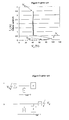
- FIG. 1 shows a current voltage curve of a typical prior art bipolar ESD device, having a breakdown voltage V bd of about 65V, a trigger voltage V t of about 95V and a holding voltage V h of about 40V.
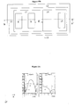
- on-chip ESD protection circuits are added to the input/output pads (I/O) (1) and supply pads (7) of the IC (2) (cf. Figure 2 ).
- the specifications of such on-chip ESD protection circuits such as triggering voltage and holding voltage are different for an Input/Output structure (I/O-port) and a power supply.
- I/O-port Input/Output structure
- a voltage peak V p or discharge on the input bonding pad (1) transferred to the chip (2) must be limited in order to prevent damage of the input of subsequent devices and circuits (2).
- the breakdown voltage V bd and trigger voltage V t such ESD device must be less than a specified maximum voltage V max .
- a power supply line providing power from the supply pad (7) to the circuit (2), as shown in figure 2b must maintain a high enough voltage, to prevent unwanted switching off of a circuit due a voltage drop on this supply line.
- Table 1 summarises typical requirements for an ESD structure used in I/O and power supply of an integrated circuit to be used in automotive applications. The corresponding ESD protections are nowadays designed for each application or circuit.
- WO-A-99/21229 a self-triggered bipolar device which is used as ESD protection device in smart power technology.
- WO-A-99/21229 describes a lateral bipolar device used as an electrostatic discharge device.
- the collector of this bipolar device consists of a highly doped region and a lowly doped region adjacent to the base region.
- the voltage applied to the collector electrode at which this bipolar device triggers depends on the width of this lowly doped collector region.
- the width of this lowly doped collector region is a layout parameter which can be predetermined for selecting a desired trigger voltage of the bipolar device.
- the holding voltage of the bipolar device is however substantially independent from this parameter.
- the (npn) ESD protection device comprises a first highly p-doped region provided with a base contact, a first highly n-doped region provided with a collector contact and, in between, a second highly n-doped region provided with an emitter contact.
- the first highly p-doped region and the second highly n-doped region are applied in a weakly p-doped region.
- This weakly p-doped region has a lateral overlap which extends towards the first highly n-doped region, the lateral overlap having a width "d".
- the first highly n-doped region is applied in a weakly n-doped region.
- This weakly n-doped region and the weakly p-doped region are applied in a more weakly n-doped region.
- a highly n-doped buried layer (BLN) is located underneath the more weakly n-doped region and extends below at least a portion of the weakly n-doped region and at least a portion of the weakly p-doped region.
- the first highly p-doped region has a doping concentration above that of the weakly p-doped region.
- the first highly n-doped region has a doping concentration above that of the weakly n-doped region, which in turn has a doping concentration above that of the more weakly n-doped region.
- the highly n-doped buried layer (BLN) has a doping concentration above that of the weakly n-doped region. Because of its structure, the ESD device is provided for enabling a lateral current component from the first highly n-doped region in the direction of the second highly n-doped region and a vertical current component from the BLN in the direction of the second highly n-doped region.
- the layout parameter "d” is varied. It has been found that by varying the "d” parameter, it can be determined how electrical current will flow through the device in holding state, i.e. after the breakthrough voltage is reached and the device snaps back to the holding voltage. At smaller values of "d”, the current will flow more laterally, i.e. more near the surface of the device, than at larger values of "d", at which the current will flow more vertically. In other words, for smaller values of "d” the lateral current component is favoured, whereas for larger values of "d” the vertical current component is favoured.
- the "d" parameter enables a selection in a range of obtainable holding voltages for the ESD device of the invention in the conductive state.
- the more weakly n-doped region separates the weakly n-doped region from the BLN.
- a sinker region is omitted in the device of the invention.
- Such a sinker region is used in the prior art to connect the weakly n-doped region with the BLN and forms a reduction in the collector resistance of the device.
- this reduction in the collector resistance does not provide an adequate solution in the device of the invention, as this leads a predominancy of the vertical current component.
- the "d" parameter would have to be chosen so small in order to make the lateral current component dominant, that there would be substantially no lateral overlap of the weakly p-doped region left.
- the width "d" of the lateral overlap would have to be reduced to a phisically unobtainable size. So if a sinker region were present, it would become substantially impossible to select a ratio for the lateral and vertical currect components and as such substantially impossible to obtain a desired holding voltage of the device by choosing a value for "d".
- the implementation of a sinker region in an ESD device requires a full BiCMOS process. Omitting the sinker region has the economic advantage that the device of the invention can be produced in a simplified or reduced BiCMOS process, which makes it possible to reduce the number of patterning and implementation steps.
- An advantage of the present invention is that it offers an ESD structure with which a desired holding voltage can be easily achieved by adapting the layout. As this can be achieved by changing only one layout parameter, this offers an easy, flexible and cost-effective solution.
- the device can be seen as comprising a lateral transistor and a vertical transistor.
- the lateral transistor enables the lateral current component and is formed by the sequence of the second highly n-doped region, the weakly p-doped region, the weakly n-doped region and the first highly n-doped region.
- the vertical transistor enables the vertical current component and is formed by the sequence of the second highly n-doped region, the weakly p-doped region, the more weakly n-doped region and the highly n-doped buried layer.
- the width "d" of the lateral overlap of the weakly p-doped region it can be determined which of these two transistors "snaps back" first, i.e. which of these two transistors becomes active at the triggering voltage of the device and will, as a result, determine the holding voltage of the device in use.
- "d" is chosen such that the holding voltage of the device is determined by either the lateral or the vertical transistor. Choosing "d” in such a way that the holding voltage is only determined by either the lateral or the vertical transistor has the advantage that the stability of the holding voltage can be enhanced, i.e. that the current dependency of the holding voltage can be reduced.
- the holding voltage is determined by the lateral transistor, whereas for higher values of "d", the holding voltage is determined by the vertical transistor.
- the lateral and vertical transistors are in competition, which leads to a holding voltage having an intermediate value.
- the more weakly n-doped region separates the weakly p-doped region and the weakly n-doped region by a first predetermined distance "t".
- This distance "t" can be chosen in function of the trigger voltage of the device in use.
- a second highly p-doped region is provided in the lateral overlap of the weakly p-doped region.
- the second highly p-doped region has a doping concentration above that of the weakly p-doped region.
- This second highly p-doped region changes the carrier density in the lateral overlap and hence the gain of the lateral device.
- Providing the second highly p-doped region in the lateral overlap has the same effect as choosing a larger value for the width "d" of the lateral overlap.
- providing the second highly p-doped region allows a reduction of the width "d" of the lateral overlap in comparison with a lateral overlap without such second highly p-doped region. This has the advantage that the size of the ESD device of the invention can be reduced.
- the buried layer is laterally separated from the second highly n-doped region by a second predetermined distance "b".
- a lateral separation may also be applied on the other side of the buried layer, namely by laterally separating the buried layer from the first highly n-doped region by a third predetermined distance "c".
- the lateral separations "b” and “c” may also be combined. Laterally separating the buried layer on one or both sides involves an increase in the collector resistance of the vertical bipolar and as such forms an alternative way of controlling the holding voltage of the device. In other words, the distances "b” and “c” form further parameters for tuning the holding voltage of the device in the conductive state.
- the weakly p-doped region preferably separates the first highly p-doped region from the second highly n-doped region.
- the first highly p-doped region and the second highly n-doped region may however also contact each other.
- the weakly p-doped region contacts the weakly n-doped region, i.e. the "t"-parameter is chosen zero.
- the "t"-parameter is chosen zero.
- the invention also relates to devices comprising first and second ESD devices according to one of the above described embodiments, the width "d" of the overlap of the first ESD device being different from that of the second ESD device. In this way a device is provided which is suitable for sustaining two different holding voltages, one being determined by the first ESD device and the other by the second ESD device.
- Figure 1 shows the collector current-voltage (I/V) curve of a prior art bipolar ESD device showing typical ESD performance parameters.
- Figure 2 shows a schematic representation of an I/O structure (a) and a power supply structure (b) known from the prior art.
- Figure 3 shows a schematic cross-section of a lateral bipolar device manufactured in a prior art full BiCMOS process.
- Figure 4a shows a schematic cross-section of a lateral bipolar device manufactured in a simplified BiCMOS process, according to the present invention.
- Figures 4b-c show the doping profiles in vertical direction of the device of figure 4a .
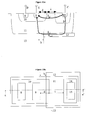
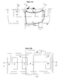
- Figure 5a shows a schematic cross-section of a lateral bipolar device manufactured in a simplified BiCMOS process, according to the present invention, in which the electronic elements of the ESD structure are indicated.
- Figure 5b shows a schematic top view of the device shown in figure 5a , A-A' being the line on which the cross section of figure 5a is taken.
- Figure 6 shows an electrical equivalent scheme of the embodiment of figure 5a .
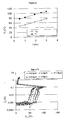
- Figure 7 shows the collector current I c (A) - collector voltage V c (V) curve illustrating influence of the layout parameter "d" on the electrical behaviour of an embodiment of the ESD structure according to the invention.
- Figure 8 shows the breakdown voltage and the trigger voltage dependence on the layout parameter "t" of an embodiment of the ESD structure according to the invention.
- Figure 9 shows the collector current-voltage (I/V) curve illustrating influence of the layout parameter "t" on the electrical behaviour of the ESD structure according to the invention.
- Figure 10a shows a schematic cross-section of a lateral bipolar device manufactured in a simplified BiCMOS process, according to the present invention, the device having a further highly p-doped region.
- Figure 10b shows a schematic top view of the device shown in figure 10a , A-A' being the line on which the cross section of figure 10a is taken.
- Figure 11a shows a schematic cross-section of a lateral bipolar device manufactured in a simplified BiCMOS process, according to the present invention, the device being modified by a further layout parameter "b".
- Figure 11b shows a schematic top view of the device shown in figure 11a , A-A' being the line on which the cross section of figure 11a is taken.
- Figure 13b shows a schematic top view of the device shown in figure 13a , A-A' being the line on which the cross section of figure 13a is taken.
- Figure 13c shows the doping profiles in vertical direction of the device of figure 13a .
- Figure 14b shows a schematic top view of the device shown in figure 14a , A-A' being the line on which the cross section of figure 14a is taken.
- Figure 15a shows a schematic cross-section of a lateral bipolar device manufactured in a simplified BiCMOS process, according to the present invention, the device being modified by the parameter "c".
- Figure 15b shows a schematic top view of the device shown in figure 15a , A-A' being the line on which the cross section of figure 15a is taken.
- Table 1 gives an overview of typical ESD specifications as used in automotive applications.
- an ESD structure comprising two bipolar devices, processed in a modified BiCMOS technology, is disclosed.
- a 0.7 ⁇ m analogue BiCMOS technology with additional high voltage, memory and bipolar modules will be used.
- This BiCMOS technology is not optimised towards bipolar characteristics for reasons of cost and process time.
- the present invention is however also applicable to other BiCMOS technologies having larger or smaller, even submicron, dimensions.
- ESD structures comprising npn bipolar devices are used, but the present invention is also applicable to ESD structures comprising pnp bipolar devices, by changing n-type regions with p-type regions and vice-versa.
- TLP Transmission Line Pulse
- It2 A mm 2
- this stepwise increase of the leakage current of the device results in a two- to five-fold increase or even more of the leakage current.
- the leakage current of the device under test is measured at a fixed voltage, e.g. at the supply voltage, which is about 5V for a 0.7 ⁇ m technology.
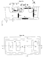
- Figure 3 outlines the cross-section of a prior art lateral bipolar device manufactured in a full BiCMOS process.
- the device is implemented on a p-type substrate 13 and comprises a first highly p-doped region 8 provided with a base contact B, a first highly n-doped region 15 provided with a collector contact C and, in between, a second highly n-doped region 9 provided with an emitter contact E.
- the first highly p-doped region 8 is referred to as the base contact region 8
- the first highly n-doped region 15 as the collector contact region 15
- the second highly n-doped region 9 as the emitter region 9.
- the base contact region 8 and the emitter region 9 are applied in a weakly p-doped region 10, referred to as the p-body 10, which separates them from each other.
- the collector region of the bipolar device comprises in fact several n-type regions doped to a different level: the highly n-doped collector contact region 15 is applied in a weakly n-doped region 14, referred to as the n-well 14; underneath the n-well 14 a sinker region 20 is provided of about the same doping level as the n-well 14; a highly n-doped buried layer (BLN) 12 contacts and extends below the sinker region 20; the BLN 12 further extends below a more weakly n-doped region 11, referred to as the n-tub 11, which separates the p-body 10 from the BLN 12, the n-well 14 and the sinker region 20.
- the highly n-doped collector contact region 15 is applied in a weakly n-doped
- Figure 4a outlines the cross-section of a first embodiment of the bipolar device according to the invention.
- a characteristic feature of the device according to the present invention is the absence of the sinker region 20 ( figure 3 ).
- the sinker 20 is used to decrease the collector resistance of the bipolar device.
- the omittance of the sinker 20 advantageously increases the difference between the resistance in lateral direction, i.e. directly between the emitter region 9 and the collector contact region 15, and the resistance in vertical direction, i.e. via the BLN 12, in the conductive state of the device.
- the increase in difference between the resistances has shown that the "d"-parameter, which is defined as the width of the lateral overlap of the p-body 10 towards the collector contact region 15, can efficiently be used to influence the ratio between the lateral current component I cl and the vertical current component I cv of the device in the conductive state, and consequently its holding voltage.
- the bipolar structure of the invention suitable for use as ESD protection device, providing a wide range of selectable holding voltages by varying only a single layout parameter, namely the "d" parameter.
- the omittance of the sinker region 20 has the economic advantage that the device can be manufactured in a simplified or reduced BiCMOS process, with a reduced number of patterning and implantation steps with respect to a full BiCMOS process.
- the bipolar device shown in figure 4a comprises a lateral bipolar device, which enables the lateral current component I cl , and a parasitic vertical bipolar device, which enables the vertical current component I cv .
- the lateral bipolar device is formed by the sequence of the emitter region 9, the p-body 10, the n-well 14 and the collector contact region 15.
- the vertical bipolar device is formed by the sequence of the emitter region 9, the p-body 10, the n-tub 11 and the BLN 12.
- the parameter "d" i.e. the width of the lateral overlap of the p-body 10 towards the collector contact region 15, is preferably chosen such that either the lateral current component I cl is dominant, or the vertical current component I cv is dominant.
- the "d” parameter is preferably chosen such that the holding voltage of the device in the conductive state is determined by either the lateral transistor or the vertical transistor.
- the lateral current component I cl is dominant and the holding voltage of the device in the conductive state is determined by the lateral transistor.
- the vertical current component I cv is dominant and the holding voltage of the device in the conductive state is determined by the vertical transistor.
- the lateral and vertical current components I cl and I cv are in competition, with a holding voltage of the device in use being mainly determined by the vertical transistor for lower currents and mainly determined by the lateral transistor for higher currents (see figure 7 ).
- the p-body region 10 separates the base contact region 8 from the emitter region 9.
- the base contact region 8 and the emitter region 9 may however also contact each other, in which case the base and emitter contacts B and E may be constructed as a single contact (not shown).
- the p-body 10 and the n-well are seperated from each other by the n-tub 11. They may however also contact each other, as is for example shown in the embodiments of figures 13-15 .
- the p-body 10 is referred to as the p-well 17, which is also a weakly p-doped region, but which specifies the difference in structure with respect to the other embodiments of the invention (shown in figures 5-11 ).
- the doping level of the weakly doped p-regions, i.e. p-well 17 or p-body 10 will be in the range of 1e16 to 1e17 cm -3 .
- the doping level of the weakly doped n-regions, i.e. n-tub 11 will be in the range of 1e15 to 1e16 cm -3 .
- Highly doped regions, such as the emitter n+ 9 and base contact p+ 8 regions will be doped above a doping level of 1e19 cm -3 .
- the n+ buried layer 12 will be in the range of 1e16 to 1e18 cm -3 .
- Typical peak concentrations of the various doping regions of the 0.7 ⁇ m BiCMOS technology used are:
- Figures 4b-c show the doping profiles in vertical direction of the devices.
- Figure 4b shows the metallurgical junction (i) between the base contact region 8 - p-body region 10 on the one hand and the n-tub 11- BLN layer 12 on the other hand.
- the metallurgical junction (j) between the BLN layer 12 and the p-substrate 13 is also shown.
- the bends in the graph show the transitions from one region to another, e.g. the transition (I) from the p+ region 8 to the p-body 10. Each bend in the graph represents a change in concentration.
- the bend at (k) also represents the difference in doping level between the n-tub 11 and the BLN 12. In the BLN 12, the graph peaks towards a doping level on the order of 1e19.
- Figure 4c shows the metallurgical junction (m) between the emitter contact region 9 and the p-body region 10 and between (i) the p-body 10 and the n-tub region 11.
- the metallurgical junction (j) between the BLN layer 12 and the p-substrate 13 is also shown.
- the change (k) in concentration between the n-tub 11 and the BLN 12 is indicated.
- FIGs 5a and 5b outline the electrical equivalent structure of the lateral and vertical device shown in figure 4a .
- the lateral device has a basewidth "d" defined by the lateral distance between the n+ contact region 9 forming the emitter and the n-tub region 11.
- the collector resistance of the lateral device is determined by the resistance R cl1 of the weakly doped n-tub region 11 and by the resistance R cl2 of the more weakly doped n-well region 14.
- the vertical device on the other hand has a vertical basewidth W defined by the difference in depth between the p-body 10 base region and the n+ contact region 9 forming the emitter. This vertical basewidth is fixed for a given process for producing the device.
- the collector resistance of the vertical device is determined by the resistance R cv1 and R cv3 of the weakly doped n-tub region 11, by the resistance R cvl2 of the a highly doped buried layer region (BLN) 12 and by the resistance R cv2 of the weakly doped n-well region 14.
- both devices are connected with a common base, the characteristics of both base regions can be different.
- the base widths d and W can differ as can be seen in figures 4 and 5 , but also the doping levels can be different e.g. due the vertical dopant profile of the p-body.
- the two bipolar devices have a common base, emitter and collector connection as shown in the simplified electrical equivalent structure of the ESD device given in figure 6 .
- the base and emitter are electrically connected to the same potential, in this example the ground potential, while the collector is electrically connected to a bond pad (1 or 7).
- the numbering of each resistor refers to the corresponding dopant region.
- the highly n-doped layer 12 is at least located underneath or at least overlaps the emitter region 9 and the collector region 15.
- the base width d of the lateral device is varied resulting in a corresponding change of holding voltage of the ESD structure.
- Figure 7 shows the collector current-voltage characteristics of the ESD structure according to the present invention obtained by TLP for three different lateral base width "d" values: 3 ⁇ m, 10 ⁇ m and 20 ⁇ m.
- the ESD device may support the same current at a lower voltage and the first electrical snapback (V t1 in figure 7 ) occurs. At that moment, the lateral bipolar device turns on, but the device is still in a low-current bipolar mode. The impact ionisation region is still located at the p-body/n-tub junction near the surface of the substrate (13) in which the ESD structure is formed.
- the base push-out effect arises. This effect appears when the mobile charge density at the depletion region of the base 10 - collector 11 junction becomes higher than the fixed charge density in this depletion region.
- the base push-out results in a lateral extension of the base region into the n-tub 11, by which the ionisation region is pushed away from the p-body 10/n-tub 11 junction towards the collector n-well 14/n+ 15 gradient.
- the multiplication or impact ionisation rate is higher compared to the lower doped n-tub region 11, so a lower electric field is enough to obtain the same avalanche current in the ESD device.
- the collector voltage then drops to bring the device in a second strong and purely electrical snapback state (V t2 in figure 7 ).
- the device finally stabilises itself at a very low holding voltage of 5V to 10V (V hl in figure 7 ). This low holding voltage is thus related to the extremely high impact ionisation occurring at the n+ collector region 14-15.
- the distance "d" can be changed by changing the layout.
- the vertical dimensions of the various dopant regions are process dependent and are fixed for a given process, e.g. given implant conditions and thermal budget.
- the current is now mainly flowing vertically via the BLN. Further, as the bipolar in the low-current regime is conducting vertically, no base push-out is possible laterally towards the n-well. If the collector current increases the base push-out occurs in the vertical direction, following the current flow, pushing the impact ionisation towards the BLN (12). When the impact ionisation region reaches the BLN-layer, again a second snapback occurs since the BLN layer (12) is much higher doped than the n-tub (11) part of the vertical collector region.
- the type of the bipolar-turn-on can be chosen and selected between the lateral and the vertical bipolar device, and associated to the bipolar conduction, the base push-out establishes itself differently. This leads to a different snapback as the region of reallocation and the amount of the impact ionisation is different.
- the holding voltage of the ESD structure is controlled by the bipolar conduction path. Which bipolar conduction path will be followed after triggering of the ESD structure is determined by the design parameter "d”. A change in "d” will change the ratio in total current gain of the lateral and vertical bipolar device. The bipolar device yielding the highest collector current at a given voltage will dominate the current flow and determine the holding voltage.
- the collector current of bipolar device is determined by the impact ionisation rate, the current gain and the total collector resistance of the device.
- the feedback mechanism of each transistor is determined by the corresponding current gain and collector resistance.
- the current gain ⁇ l of the lateral device is determined by the concentration of p-body base region (10), n-tub (11)/n-well (14) collector concentration and the base width d.
- the current gain ⁇ v of the vertical device is determined by the concentration of the p-body base region (10), the concentration of the n-tub (11)/BLN (12) collector region and the base width W, which can easily by varied.
- Each impurity region will have a dopant gradient towards the p-substrate.
- both lateral and vertical bipolars are in competition with each other.
- the current increases, it does for both the bipolars, simultaneously increasing the base push-out effect in both directions (lateral and vertical).
- the lateral bipolar is more enhanced than the vertical one leading to a larger proportion of current through the lateral than the vertical.
- the lateral bipolar is becoming more and more dominant, it allows the voltage to drop from the vertical bipolar holding voltage to the lateral bipolar holding voltage, as shown on figure 7 by V hi .
- the vertical bipolar device allows a better power dissipation and hence a good ESD robustness as the collector current I cl is deeply spread.
- the vertical device will have a larger holding voltage V hv , which in combination with this lower current density will give a small thermal dissipation , i.e. product of voltage and current.
- the lateral device will have a lower holding voltage V hl , but have a higher current density, as the collector current I cv is only flowing at the surface.
- the large base device, d 20 ⁇ m, in which the holding voltage V hv is determined by vertical device, with a large holding voltage (40V) is a good protection device for supply buses and if the power dissipation is higher due to the high holding voltage, the structure is still robust since the current is spread deeply into the device.
- the base width "d" of the lateral device is modulated by introducing an second highly p-doped region 16 in the base region overlapping the emitter region 9.
- a base width "d" of 20 to 30 ⁇ m is required for the given BiCMOS technology in order to have the vertical bipolar device switched on and have a high holding voltage.
- the area of the ESD structure will be very large for a high holding voltage.
- the consequence of increasing "d" for a higher holding voltage is that the size of the protection structure suffers from the competition between the lateral and the vertical bipolar transistor. As a result, it is desired to reduce the operation of the lateral device without increasing its physical base width "d".
- This size issue can be overcome by introducing the floating, i.e. unbiased, p+ diffusion region 16, with the purpose of deteriorating the working of the lateral transistor while keeping a high holding voltage. Due to this floating p+ diffusion region 16, the electrical base width d e of the lateral device is larger than its physical or layout-determined base width d. The introduction of the floating p+ diffusion region 16 heavily dopes the base region 10 of the lateral transistor without impacting the profile of the vertical device. The direct consequence is that the current gain of the lateral transistor is now worse and allows the vertical one to trigger first. The cross section is shown in fig 10a and the corresponding top view in figure 10b . The introduction of this highly doped p+ region 16 only requires a change in the layout of the device.
- the holding voltage of the device of the invention can be further modified as shown in the embodiments of figures 11a-b and 14a-b .
- the highly n-doped layer 12 is at least located underneath the collector contact region 15 and is spaced apart from the emitter region 9 by a lateral distance "b".
- the feedback mechanism of the bipolar device is modified, now by varying or modulating the vertical collector resistance. This varying is again obtained by only changing a layout parameter, i.e. the spacing "b" between the BLN region 12 and the emitter region 9.
- the same effect can be achieved by providing the spacing on the other side of the BLN 12, i.e. spacing the BLN 12 apart from the collector contact region 15 by a lateral distance "c", as is for example shown in the embodiment of figures 15a-b . Both parameters "b” and "c" may also be combined.
- the embodiment shown in figures 11a-b is very similar to the embodiment of figures 4 and 5 except that the BLN layer 12 is partly omitted.
- the parameter "b" defines the region of the omission.
- the R CV2 portion of the vertical collector resistance is decreased, which was already low resistive, and the portion R CV1 is increased which was high resistive, so that the total collector resistance of the vertical device is increased.
- This modulation of the collector resistance of the vertical device will determine which device, lateral or vertical, is turned on and if the vertical device is turned on which holding voltage is obtained. This holding voltage will depend on the given current gain and collector resistance.
- the doping level of the base region is changed without changing the given BiCMOS process.
- the p-body 10 is replaced by a p-well 17.
- the p-well is touching the n-well and the parameter "t" has no meaning anymore.
- the p-well is defined as the inverse of the n-well and only the n-well regions are layouted, while the p-well regions will be calculated by the design program.
- the trigger voltage can not be modified and is fixed for a given technology.
- the parameter "d” remains valid and is also used to control the holding voltage as explained above with regard to the other embodiments of the device of the invention.
- a full highly n-doped layer 12 is present underneath and extending from the emitter region 9 to the collector region 15.
Landscapes
- Bipolar Transistors (AREA)
- Bipolar Integrated Circuits (AREA)
- Semiconductor Integrated Circuits (AREA)
Claims (10)
- Dispositif de protection ESD (contre les décharges électrostatiques) comprenant :- une première région hautement dopée p (8) pourvue d'un contact de base (B),- une première région hautement dopée n (15) pourvue d'un contact collecteur (C),- une deuxième région hautement dopée n (9) pourvue d'un contact émetteur (E) et située entre la première région hautement dopée p (8) et la première région hautement dopée n (15),- la première région hautement dopée p (8) et la deuxième région hautement dopée n (9) étant appliquées dans une région faiblement dopée p (10 ; 17) qui a un chevauchement latéral s'étendant de la deuxième région hautement dopée n (9) en direction de la première région hautement dopée n (15),- le dispositif ayant une largeur de base latérale prédéterminée (d) définie comme la largeur dudit chevauchement latéral mesuré à partir de la deuxième région hautement dopée n dans la direction de la première région hautement dopée n (15),- la première région hautement dopée n (15) étant appliquée dans une région faiblement dopée n (14),- la région faiblement dopée p (10 ; 17) et la région faiblement dopée n (14) étant appliquées dans une région plus faiblement dopée n (11),- et une couche hautement dopée n enfouie (12) située en dessous de la région plus faiblement dopée n (11) et s'étendant en dessous d'au moins une partie de la région faiblement dopée n (14) et d'au moins une partie de la région faiblement dopée p (10 ; 17),- la première région hautement dopée p (8) ayant une concentration de dopage supérieure à celle de la région faiblement dopée p (10 ; 17),- la première région hautement dopée n (15) ayant une concentration de dopage supérieure à celle de la région faiblement dopée n (14) qui, à son tour, a une concentration de dopage supérieure à celle de la région plus faiblement dopée n (11),- la région hautement dopée n enfouie (12) ayant une concentration de dopage supérieure à celle de la région faiblement dopée p (10 ; 17),- le dispositif étant prévu pour activer une composante latérale de courant (Icl) en provenance de la première région hautement dopée n (15) dans la direction de la deuxième région hautement dopée n (9) et une composante verticale de courant (Lcv) en provenance de la première région hautement dopée n (9) en passant par la première couche enfouie (12) dans la direction de la deuxième région hautement dopée n (9),- seule la région plus faiblement dopée n (11) étant située entre la région faiblement dopée n (14) et la couche enfouie (12),
caractérisé en ce que- la largeur de base latérale prédéterminée (d) est déterminée en fonction d'un rapport prédéterminé entre la composante latérale de courant (Lcl) et la composante verticale de courant (Lcv). - Dispositif ESD selon la revendication 1, caractérisé en ce qu'une première séquence de la deuxième région hautement dopée n (9), la première région faiblement dopée p (10 ; 17), la région faiblement dopée n (14) et la première région hautement dopée n (15) forme un transistor latéral pour activer la composante latérale de courant (Lcv) et en ce qu'une deuxième séquence de la deuxième région hautement dopée n (9), la région faiblement dopée p (10 ; 17), la région plus faiblement dopée n (11) et la couche hautement dopée n enfouie (12) forme un transistor vertical pour activer la composante verticale de courant (Lcv).
- Dispositif ESD selon la revendication 1 ou 2, caractérisé en ce que la région plus faiblement dopée n (11) sépare la région faiblement dopée p (10 ; 17) et la région faiblement dopée n (14) par une première distance prédéterminée (t), ladite distance (t) étant déterminée en fonction d'une tension de déclenchement prédéterminée (Vt) du dispositif en service.
- Dispositif ESD selon l'une quelconque des revendications 1 - 3, caractérisé en ce qu'une deuxième région hautement dopée p (16) est appliquée dans le chevauchement latéral de la région faiblement dopée p (10 ; 17), la deuxième région hautement dopée p (16) ayant une concentration de dopage supérieure à celle de la région faiblement dopée p (10 ; 17).
- Dispositif ESD selon l'une quelconque des revendications 1 - 4, caractérisé en ce que la couche enfouie (12) est séparée latéralement de la deuxième région hautement dopée n (9) par une deuxième distance prédéterminée (b).
- Dispositif ESD selon l'une quelconque des revendications 1 - 5, caractérisé en ce que la couche enfouie (12) est séparée latéralement de la première région hautement dopée n (15) par une troisième distance prédéterminée (c).
- Dispositif ESD selon l'une quelconque des revendications 1 - 6, caractérisé en ce que la région faiblement dopée p (10 ; 17) sépare la première région hautement dopée p (8) de la deuxième région hautement dopée n (9).
- Dispositif ESD selon l'une quelconque des revendications 1 - 7, caractérisé en ce que la région faiblement dopée p (17) entre en contact avec la région faiblement dopée n (14).
- Dispositif ESD selon l'une quelconque des revendications 1 - 8, caractérisé en ce que les régions dopées p sont remplacées par des régions dopées n et vice-versa.
- Dispositif comprend des premier et deuxième dispositifs ESD selon l'une quelconque des revendications 1 - 9, la largeur de base latérale (d) du premier dispositif ESD étant différente de celle du deuxième dispositif ESD.
Priority Applications (1)
| Application Number | Priority Date | Filing Date | Title |
|---|---|---|---|
| US10/131,924 US6707110B2 (en) | 2001-04-27 | 2002-04-25 | Layout configurable electrostatic discharge device for integrated circuits |
Applications Claiming Priority (2)
| Application Number | Priority Date | Filing Date | Title |
|---|---|---|---|
| US28682601P | 2001-04-27 | 2001-04-27 | |
| US286826P | 2001-04-27 |
Publications (2)
| Publication Number | Publication Date |
|---|---|
| EP1255301A1 EP1255301A1 (fr) | 2002-11-06 |
| EP1255301B1 true EP1255301B1 (fr) | 2013-03-27 |
Family
ID=23100331
Family Applications (1)
| Application Number | Title | Priority Date | Filing Date |
|---|---|---|---|
| EP02290153A Expired - Lifetime EP1255301B1 (fr) | 2001-04-27 | 2002-01-21 | Dispositiv de protection contre les décharges électrostatiques à layout configurable pour circuits integrés |
Country Status (2)
| Country | Link |
|---|---|
| US (1) | US6707110B2 (fr) |
| EP (1) | EP1255301B1 (fr) |
Cited By (1)
| Publication number | Priority date | Publication date | Assignee | Title |
|---|---|---|---|---|
| CN103902761A (zh) * | 2014-03-10 | 2014-07-02 | 中航(重庆)微电子有限公司 | 一种沟槽型mos器件的导通电阻的仿真分析方法 |
Families Citing this family (14)
| Publication number | Priority date | Publication date | Assignee | Title |
|---|---|---|---|---|
| US6717219B1 (en) * | 2002-04-12 | 2004-04-06 | National Semiconductor Corporation | High holding voltage ESD protection structure for BiCMOS technology |
| DE102005028919B4 (de) * | 2005-06-22 | 2010-07-01 | Infineon Technologies Ag | Verfahren zum Herstellen eines elektronischen Bauelementes und elektronisches Bauelement |
| US20070023866A1 (en) * | 2005-07-27 | 2007-02-01 | International Business Machines Corporation | Vertical silicon controlled rectifier electro-static discharge protection device in bi-cmos technology |
| US8022505B2 (en) * | 2006-03-13 | 2011-09-20 | Freescale Semiconductor, Inc. | Semiconductor device structure and integrated circuit therefor |
| US8928084B2 (en) * | 2007-05-04 | 2015-01-06 | Freescale Semiconductor, Inc. | ESD protection device and method of forming an ESD protection device |
| US20090032906A1 (en) | 2007-07-30 | 2009-02-05 | Infineon Technologies Austria Ag | Electro static discharge device and method for manufacturing an electro static discharge device |
| US7773356B2 (en) * | 2008-03-19 | 2010-08-10 | Fairchild Korea Semiconductor Ltd | Stacked SCR with high holding voltage |
| US7868387B2 (en) * | 2008-06-13 | 2011-01-11 | Analog Devices, Inc. | Low leakage protection device |
| US8982516B2 (en) | 2010-11-12 | 2015-03-17 | Freescale Semiconductor, Inc. | Area-efficient high voltage bipolar-based ESD protection targeting narrow design windows |
| US8390092B2 (en) * | 2010-11-12 | 2013-03-05 | Freescale Semiconductor, Inc. | Area-efficient high voltage bipolar-based ESD protection targeting narrow design windows |
| KR101834520B1 (ko) * | 2012-04-25 | 2018-03-06 | 에스케이하이닉스 주식회사 | 정전 방전 보호 소자 |
| US9893050B2 (en) | 2015-06-30 | 2018-02-13 | Nxp Usa, Inc. | ESD protection structure |
| KR20190140220A (ko) | 2018-06-11 | 2019-12-19 | 에스케이하이닉스 주식회사 | 정전기 방지 회로를 구비하는 반도체 집적 회로 장치 및 그 제조방법 |
| US12507485B2 (en) * | 2023-06-13 | 2025-12-23 | Amazing Microelectronic Corp. | Bipolar junction transistor with lateral and vertical conducting paths |
Family Cites Families (7)
| Publication number | Priority date | Publication date | Assignee | Title |
|---|---|---|---|---|
| JPS5153483A (fr) * | 1974-11-06 | 1976-05-11 | Hitachi Ltd | |
| US4463369A (en) * | 1981-06-15 | 1984-07-31 | Rca | Integrated circuit overload protection device |
| IT1253682B (it) * | 1991-09-12 | 1995-08-22 | Sgs Thomson Microelectronics | Struttura di protezione dalle scariche elettrostatiche |
| US5268588A (en) * | 1992-09-30 | 1993-12-07 | Texas Instruments Incorporated | Semiconductor structure for electrostatic discharge protection |
| US5602409A (en) * | 1995-07-13 | 1997-02-11 | Analog Devices, Inc. | Bidirectional electrical overstress protection circuit for bipolar and bipolar-CMOS integrated circuits |
| DE19746410C2 (de) | 1997-10-21 | 1999-11-25 | Bosch Gmbh Robert | ESD-Schutzvorrichtung für integrierte Schaltungen |
| DE19917155C1 (de) * | 1999-04-16 | 2000-06-21 | Bosch Gmbh Robert | Schutzvorrichtung gegen elektrostatische Entladungen |
-
2002
- 2002-01-21 EP EP02290153A patent/EP1255301B1/fr not_active Expired - Lifetime
- 2002-04-25 US US10/131,924 patent/US6707110B2/en not_active Expired - Lifetime
Cited By (1)
| Publication number | Priority date | Publication date | Assignee | Title |
|---|---|---|---|---|
| CN103902761A (zh) * | 2014-03-10 | 2014-07-02 | 中航(重庆)微电子有限公司 | 一种沟槽型mos器件的导通电阻的仿真分析方法 |
Also Published As
| Publication number | Publication date |
|---|---|
| EP1255301A1 (fr) | 2002-11-06 |
| US6707110B2 (en) | 2004-03-16 |
| US20030006464A1 (en) | 2003-01-09 |
Similar Documents
| Publication | Publication Date | Title |
|---|---|---|
| EP1255301B1 (fr) | Dispositiv de protection contre les décharges électrostatiques à layout configurable pour circuits integrés | |
| US8633509B2 (en) | Apparatus and method for transient electrical overstress protection | |
| KR100305238B1 (ko) | Esd보호를위한실리콘제어정류기 | |
| US7919817B2 (en) | Electrostatic discharge (ESD) protection applying high voltage lightly doped drain (LDD) CMOS technologies | |
| US8503141B2 (en) | Transient voltage suppressor (TVS) with improved clamping voltage | |
| US8338915B2 (en) | Circuit configuration and manufacturing processes for vertical transient voltage suppressor (TVS) and EMI filter | |
| US6909149B2 (en) | Low voltage silicon controlled rectifier (SCR) for electrostatic discharge (ESD) protection of silicon-on-insulator technologies | |
| US6194764B1 (en) | Integrated semiconductor circuit with protection structure for protecting against electrostatic discharge | |
| US20050212051A1 (en) | Low voltage silicon controlled rectifier (SCR) for electrostatic discharge (ESD) protection of silicon-on-insulator technologies | |
| US20170373158A1 (en) | Circuit configuration and manufacturing processes for vertical transient voltage suppressor (tvs) and emi filter | |
| US10205017B2 (en) | Bottom source NMOS triggered Zener clamp for configuring an ultra-low voltage transient voltage suppressor (TVS) | |
| EP1294025A2 (fr) | Circuit redresseur au silicium commande pour la protection de circuits integres contre les decharges electrostatiques | |
| US20070284667A1 (en) | Electrostatic discharge protection method and device for semiconductor device | |
| KR20080092308A (ko) | 자체 저-트리거 및 고-홀딩 전압 scr | |
| US6320232B1 (en) | Integrated semiconductor circuit with protective structure for protection against electrostatic discharge | |
| EP0312097B1 (fr) | Dispositif de protection d'entrée pour un composant semi-conducteur | |
| EP0807977A2 (fr) | Dispositif semi-conducteur comprenant des moyens de protection | |
| WO2010019336A1 (fr) | Dispositif semi-conducteur résistant aux décharges électrostatiques et aux déclenchements parasites | |
| US20070181948A1 (en) | ESD protection device | |
| WO2007038645A2 (fr) | Systemes et procedes de protection electrostatique | |
| JP5023254B2 (ja) | 集積回路の静電荷放電保護 | |
| US7023028B2 (en) | Protection structure for protection from electrostatic discharge and integrated circuit | |
| US6791808B2 (en) | Clipping device with a negative resistance | |
| US20040145022A1 (en) | Semiconductor device serving as a protecting element | |
| US20110089532A1 (en) | Integrated circuit with esd structure |
Legal Events
| Date | Code | Title | Description |
|---|---|---|---|
| PUAI | Public reference made under article 153(3) epc to a published international application that has entered the european phase |
Free format text: ORIGINAL CODE: 0009012 |
|
| AK | Designated contracting states |
Kind code of ref document: A1 Designated state(s): AT BE CH CY DE DK ES FI FR GB GR IE IT LI LU MC NL PT SE TR |
|
| AX | Request for extension of the european patent |
Free format text: AL;LT;LV;MK;RO;SI |
|
| RAP1 | Party data changed (applicant data changed or rights of an application transferred) |
Owner name: AMI SEMICONDUCTOR BELGIUM BVBA Owner name: INTERUNIVERSITAIR MICRO-ELEKTRONICA CENTRUM VZW |
|
| AKX | Designation fees paid | ||
| REG | Reference to a national code |
Ref country code: DE Ref legal event code: 8566 |
|
| 17P | Request for examination filed |
Effective date: 20030505 |
|
| RBV | Designated contracting states (corrected) |
Designated state(s): AT BE CH CY DE DK ES FI FR GB GR IE IT LI LU MC NL PT SE TR |
|
| 17Q | First examination report despatched |
Effective date: 20040211 |
|
| 17Q | First examination report despatched |
Effective date: 20040211 |
|
| RAP1 | Party data changed (applicant data changed or rights of an application transferred) |
Owner name: AMI SEMICONDUCTOR BELGIUM BVBA Owner name: IMEC |
|
| RAP1 | Party data changed (applicant data changed or rights of an application transferred) |
Owner name: SEMICONDUCTOR COMPONENTS INDUSTRIES, LLC Owner name: IMEC |
|
| GRAP | Despatch of communication of intention to grant a patent |
Free format text: ORIGINAL CODE: EPIDOSNIGR1 |
|
| GRAS | Grant fee paid |
Free format text: ORIGINAL CODE: EPIDOSNIGR3 |
|
| GRAA | (expected) grant |
Free format text: ORIGINAL CODE: 0009210 |
|
| RIN1 | Information on inventor provided before grant (corrected) |
Inventor name: GROESENEKEN, GUIDO Inventor name: GALLOPYN, GEERT Inventor name: VACARESSE, LOUIS Inventor name: DE HEYN, VINCENT Inventor name: VAN HOVE, HUGO |
|
| AK | Designated contracting states |
Kind code of ref document: B1 Designated state(s): AT BE CH CY DE DK ES FI FR GB GR IE IT LI LU MC NL PT SE TR |
|
| REG | Reference to a national code |
Ref country code: GB Ref legal event code: FG4D |
|
| REG | Reference to a national code |
Ref country code: CH Ref legal event code: EP |
|
| REG | Reference to a national code |
Ref country code: AT Ref legal event code: REF Ref document number: 603900 Country of ref document: AT Kind code of ref document: T Effective date: 20130415 |
|
| REG | Reference to a national code |
Ref country code: IE Ref legal event code: FG4D |
|
| REG | Reference to a national code |
Ref country code: DE Ref legal event code: R096 Ref document number: 60244696 Country of ref document: DE Effective date: 20130516 |
|
| RIN2 | Information on inventor provided after grant (corrected) |
Inventor name: GROESENEKEN, GUIDO Inventor name: VAN HOVE, HUGO Inventor name: VACARESSE, LOUIS Inventor name: GALLOPYN, GEERT Inventor name: DE HEYN, VINCENT |
|
| PG25 | Lapsed in a contracting state [announced via postgrant information from national office to epo] |
Ref country code: SE Free format text: LAPSE BECAUSE OF FAILURE TO SUBMIT A TRANSLATION OF THE DESCRIPTION OR TO PAY THE FEE WITHIN THE PRESCRIBED TIME-LIMIT Effective date: 20130327 |
|
| REG | Reference to a national code |
Ref country code: AT Ref legal event code: MK05 Ref document number: 603900 Country of ref document: AT Kind code of ref document: T Effective date: 20130327 |
|
| PG25 | Lapsed in a contracting state [announced via postgrant information from national office to epo] |
Ref country code: GR Free format text: LAPSE BECAUSE OF FAILURE TO SUBMIT A TRANSLATION OF THE DESCRIPTION OR TO PAY THE FEE WITHIN THE PRESCRIBED TIME-LIMIT Effective date: 20130628 Ref country code: FI Free format text: LAPSE BECAUSE OF FAILURE TO SUBMIT A TRANSLATION OF THE DESCRIPTION OR TO PAY THE FEE WITHIN THE PRESCRIBED TIME-LIMIT Effective date: 20130327 |
|
| REG | Reference to a national code |
Ref country code: NL Ref legal event code: VDEP Effective date: 20130327 |
|
| PG25 | Lapsed in a contracting state [announced via postgrant information from national office to epo] |
Ref country code: BE Free format text: LAPSE BECAUSE OF FAILURE TO SUBMIT A TRANSLATION OF THE DESCRIPTION OR TO PAY THE FEE WITHIN THE PRESCRIBED TIME-LIMIT Effective date: 20130327 |
|
| PG25 | Lapsed in a contracting state [announced via postgrant information from national office to epo] |
Ref country code: ES Free format text: LAPSE BECAUSE OF FAILURE TO SUBMIT A TRANSLATION OF THE DESCRIPTION OR TO PAY THE FEE WITHIN THE PRESCRIBED TIME-LIMIT Effective date: 20130708 Ref country code: NL Free format text: LAPSE BECAUSE OF FAILURE TO SUBMIT A TRANSLATION OF THE DESCRIPTION OR TO PAY THE FEE WITHIN THE PRESCRIBED TIME-LIMIT Effective date: 20130327 Ref country code: PT Free format text: LAPSE BECAUSE OF FAILURE TO SUBMIT A TRANSLATION OF THE DESCRIPTION OR TO PAY THE FEE WITHIN THE PRESCRIBED TIME-LIMIT Effective date: 20130729 Ref country code: AT Free format text: LAPSE BECAUSE OF FAILURE TO SUBMIT A TRANSLATION OF THE DESCRIPTION OR TO PAY THE FEE WITHIN THE PRESCRIBED TIME-LIMIT Effective date: 20130327 |
|
| PG25 | Lapsed in a contracting state [announced via postgrant information from national office to epo] |
Ref country code: CY Free format text: LAPSE BECAUSE OF FAILURE TO SUBMIT A TRANSLATION OF THE DESCRIPTION OR TO PAY THE FEE WITHIN THE PRESCRIBED TIME-LIMIT Effective date: 20130327 |
|
| PG25 | Lapsed in a contracting state [announced via postgrant information from national office to epo] |
Ref country code: DK Free format text: LAPSE BECAUSE OF FAILURE TO SUBMIT A TRANSLATION OF THE DESCRIPTION OR TO PAY THE FEE WITHIN THE PRESCRIBED TIME-LIMIT Effective date: 20130327 |
|
| PLBE | No opposition filed within time limit |
Free format text: ORIGINAL CODE: 0009261 |
|
| STAA | Information on the status of an ep patent application or granted ep patent |
Free format text: STATUS: NO OPPOSITION FILED WITHIN TIME LIMIT |
|
| PG25 | Lapsed in a contracting state [announced via postgrant information from national office to epo] |
Ref country code: IT Free format text: LAPSE BECAUSE OF FAILURE TO SUBMIT A TRANSLATION OF THE DESCRIPTION OR TO PAY THE FEE WITHIN THE PRESCRIBED TIME-LIMIT Effective date: 20130327 |
|
| 26N | No opposition filed |
Effective date: 20140103 |
|
| REG | Reference to a national code |
Ref country code: DE Ref legal event code: R097 Ref document number: 60244696 Country of ref document: DE Effective date: 20140103 |
|
| PG25 | Lapsed in a contracting state [announced via postgrant information from national office to epo] |
Ref country code: MC Free format text: LAPSE BECAUSE OF FAILURE TO SUBMIT A TRANSLATION OF THE DESCRIPTION OR TO PAY THE FEE WITHIN THE PRESCRIBED TIME-LIMIT Effective date: 20130327 Ref country code: LU Free format text: LAPSE BECAUSE OF FAILURE TO SUBMIT A TRANSLATION OF THE DESCRIPTION OR TO PAY THE FEE WITHIN THE PRESCRIBED TIME-LIMIT Effective date: 20140121 |
|
| REG | Reference to a national code |
Ref country code: CH Ref legal event code: PL |
|
| PG25 | Lapsed in a contracting state [announced via postgrant information from national office to epo] |
Ref country code: CH Free format text: LAPSE BECAUSE OF NON-PAYMENT OF DUE FEES Effective date: 20140131 Ref country code: LI Free format text: LAPSE BECAUSE OF NON-PAYMENT OF DUE FEES Effective date: 20140131 |
|
| REG | Reference to a national code |
Ref country code: IE Ref legal event code: MM4A |
|
| PG25 | Lapsed in a contracting state [announced via postgrant information from national office to epo] |
Ref country code: IE Free format text: LAPSE BECAUSE OF NON-PAYMENT OF DUE FEES Effective date: 20140121 |
|
| REG | Reference to a national code |
Ref country code: FR Ref legal event code: PLFP Year of fee payment: 15 |
|
| PG25 | Lapsed in a contracting state [announced via postgrant information from national office to epo] |
Ref country code: TR Free format text: LAPSE BECAUSE OF FAILURE TO SUBMIT A TRANSLATION OF THE DESCRIPTION OR TO PAY THE FEE WITHIN THE PRESCRIBED TIME-LIMIT Effective date: 20130327 |
|
| REG | Reference to a national code |
Ref country code: FR Ref legal event code: PLFP Year of fee payment: 16 |
|
| REG | Reference to a national code |
Ref country code: FR Ref legal event code: PLFP Year of fee payment: 17 |
|
| PGFP | Annual fee paid to national office [announced via postgrant information from national office to epo] |
Ref country code: FR Payment date: 20191219 Year of fee payment: 19 |
|
| PGFP | Annual fee paid to national office [announced via postgrant information from national office to epo] |
Ref country code: DE Payment date: 20191218 Year of fee payment: 19 Ref country code: GB Payment date: 20191223 Year of fee payment: 19 |
|
| REG | Reference to a national code |
Ref country code: DE Ref legal event code: R119 Ref document number: 60244696 Country of ref document: DE |
|
| GBPC | Gb: european patent ceased through non-payment of renewal fee |
Effective date: 20210121 |
|
| PG25 | Lapsed in a contracting state [announced via postgrant information from national office to epo] |
Ref country code: FR Free format text: LAPSE BECAUSE OF NON-PAYMENT OF DUE FEES Effective date: 20210131 |
|
| PG25 | Lapsed in a contracting state [announced via postgrant information from national office to epo] |
Ref country code: GB Free format text: LAPSE BECAUSE OF NON-PAYMENT OF DUE FEES Effective date: 20210121 Ref country code: DE Free format text: LAPSE BECAUSE OF NON-PAYMENT OF DUE FEES Effective date: 20210803 |