EP1260988A2 - Widerstands-Kreuzpunkt-Speicherbauelement mit Kalibriersteuereinheit für einen Abtastverstärker - Google Patents
Widerstands-Kreuzpunkt-Speicherbauelement mit Kalibriersteuereinheit für einen Abtastverstärker Download PDFInfo
- Publication number
- EP1260988A2 EP1260988A2 EP02253365A EP02253365A EP1260988A2 EP 1260988 A2 EP1260988 A2 EP 1260988A2 EP 02253365 A EP02253365 A EP 02253365A EP 02253365 A EP02253365 A EP 02253365A EP 1260988 A2 EP1260988 A2 EP 1260988A2
- Authority
- EP
- European Patent Office
- Prior art keywords
- rxptm
- cells
- array
- sense amplifier
- sense
- Prior art date
- Legal status (The legal status is an assumption and is not a legal conclusion. Google has not performed a legal analysis and makes no representation as to the accuracy of the status listed.)
- Withdrawn
Links
Images

Classifications
-
- G—PHYSICS
- G11—INFORMATION STORAGE
- G11C—STATIC STORES
- G11C7/00—Arrangements for writing information into, or reading information out from, a digital store
- G11C7/06—Sense amplifiers; Associated circuits, e.g. timing or triggering circuits
-
- G—PHYSICS
- G11—INFORMATION STORAGE
- G11C—STATIC STORES
- G11C11/00—Digital stores characterised by the use of particular electric or magnetic storage elements; Storage elements therefor
- G11C11/02—Digital stores characterised by the use of particular electric or magnetic storage elements; Storage elements therefor using magnetic elements
- G11C11/14—Digital stores characterised by the use of particular electric or magnetic storage elements; Storage elements therefor using magnetic elements using thin-film elements
- G11C11/15—Digital stores characterised by the use of particular electric or magnetic storage elements; Storage elements therefor using magnetic elements using thin-film elements using multiple magnetic layers
-
- G—PHYSICS
- G11—INFORMATION STORAGE
- G11C—STATIC STORES
- G11C11/00—Digital stores characterised by the use of particular electric or magnetic storage elements; Storage elements therefor
- G11C11/02—Digital stores characterised by the use of particular electric or magnetic storage elements; Storage elements therefor using magnetic elements
- G11C11/16—Digital stores characterised by the use of particular electric or magnetic storage elements; Storage elements therefor using magnetic elements using elements in which the storage effect is based on magnetic spin effect
- G11C11/161—Digital stores characterised by the use of particular electric or magnetic storage elements; Storage elements therefor using magnetic elements using elements in which the storage effect is based on magnetic spin effect details concerning the memory cell structure, e.g. the layers of the ferromagnetic memory cell
-
- G—PHYSICS
- G11—INFORMATION STORAGE
- G11C—STATIC STORES
- G11C11/00—Digital stores characterised by the use of particular electric or magnetic storage elements; Storage elements therefor
- G11C11/02—Digital stores characterised by the use of particular electric or magnetic storage elements; Storage elements therefor using magnetic elements
- G11C11/16—Digital stores characterised by the use of particular electric or magnetic storage elements; Storage elements therefor using magnetic elements using elements in which the storage effect is based on magnetic spin effect
- G11C11/165—Auxiliary circuits
- G11C11/1673—Reading or sensing circuits or methods
-
- G—PHYSICS
- G11—INFORMATION STORAGE
- G11C—STATIC STORES
- G11C29/00—Checking stores for correct operation ; Subsequent repair; Testing stores during standby or offline operation
- G11C29/02—Detection or location of defective auxiliary circuits, e.g. defective refresh counters
-
- G—PHYSICS
- G11—INFORMATION STORAGE
- G11C—STATIC STORES
- G11C29/00—Checking stores for correct operation ; Subsequent repair; Testing stores during standby or offline operation
- G11C29/04—Detection or location of defective memory elements, e.g. cell constructio details, timing of test signals
- G11C29/50—Marginal testing, e.g. race, voltage or current testing
-
- G—PHYSICS
- G11—INFORMATION STORAGE
- G11C—STATIC STORES
- G11C2207/00—Indexing scheme relating to arrangements for writing information into, or reading information out from, a digital store
- G11C2207/22—Control and timing of internal memory operations
- G11C2207/2254—Calibration
Definitions
- the present application relates to a resistive cross point memory (RXPtM) device, a method for testing for needed recalibration of a sense amplifier of such a device, and a self-calibrating RXPtM cell array chip.
- this invention relates to a resistive cross point memory (RXPtM) cell array, one example of which is a magnetic random access memory (MRAM), and to circuitry for sensing a resistive state of a memory cell in the array so as to sense a stored data value from the memory cell.
- MRAM magnetic random access memory
- this invention relates to a method and apparatus for testing for acceptable calibration of a sense amplifier which is utilized in sensing the resistance value of a memory cell and sensing a stored data value from a memory cell, and for initiating recalibration of the sense amplifier, when needed, all without destroying data stored in the memory cell.
- Magnetic Random Access Memory is a non-volatile memory that is being considered for long term data storage.
- a typical MRAM device includes an array of memory cells. Word lines extend along rows of the memory cells, and bit lines extend along columns of the memory cells. The memory cells are each located at a cross point of a word line and a bit line, and each memory cell includes two masses of magnetic material. One of the masses is magnetically fixed and the other is magnetically variable. A memory cell stores a bit of information as the orientation of relative magnetization of the fixed and variable materials. In other words, the magnetization of each memory cell at any given time assumes one of two stable orientations.
- the resistance of a memory cell varies dependent upon whether it stores a "0" or a "1" value. That is, the resistance of a memory cell is a first value "R” if the orientation of the magnetization of the fixed magnetic material and of the variable magnetic material is parallel, and the resistance of the memory cell is increased to a second value R+ ⁇ R if the orientation of the magnetization is anti-parallel.
- the orientation of the relative magnetization of a selected memory cell (and, therefore, the logic state of the memory cell) may be sensed by sensing the resistance value of the selected memory cell.
- Performing sense and write operations in MRAM devices could be orders of magnitude faster than performing sense and write operations in conventional long term storage devices, such as hard drives, for example.
- the MRAM devices could be more compact and could consume less power than hard drives and other such conventional long term data storage devices.
- sensing the resistance state of a single memory cell in an array can be unreliable. All memory cells in the array are coupled together through many parallel paths (i.e., the bit and word lines). The resistance seen at one cross point equals the resistance of the memory cell at that cross point in parallel with resistances of memory cells in the other rows and columns (again, the array of memory cells may be characterized as a cross point resistor network).
- the sense amplifier is compensated or calibrated for global factors of the memory cell array that are constant over time. These global factors include such influences as process and geometry variations (i.e., asymmetries in the circuit design and fabrication non-uniformity resulting in threshold voltage variations and resistance and capacitance variations, for example) that occur during fabrication of the memory cell array.
- process and geometry variations i.e., asymmetries in the circuit design and fabrication non-uniformity resulting in threshold voltage variations and resistance and capacitance variations, for example
- the environmental factors then existing for the RXPtM array are compensated for.
- compensation for the global factors which are constant over time does not address needed compensations for environmental parameters which change over time. These environmental parameters include such factors as operating temperature of the RXPtM array, and power supply voltage variations.
- a sense amplifier is employed to sense the resistance state of a set of RXPtM cells, and a digital value of "0" or "1" for each memory element of the set is determined by comparing individual cell sense data to an average data value using a multiple sense method.
- the sense method uses a "time value.”
- time value is meant that the resistance value of an individual RXPtM cell is determined by a current-to-time conversion when an operating voltage is applied to the RXPtM cell with a sense amplifier.
- the "average time value" (ATV) for the set of RXPtM cells is determined, and a pair of test limit values (respectively referred to as “shorts” and “opens” values are set at preferred time values of 1 ⁇ 4 ATV, and 4ATV, for example. It will be understood that other values of the "shorts” and “opens” test limit values may be utilized. However, and importantly, any memory cell of the set which has an individual time value less than or equal to the "shorts" value, or greater than or equal to the "opens” value is labeled as inoperative, and is not utilized in determining when a recalibration of the sense amplifier is necessary. That is, a shorted memory cell or an open-circuit memory cell is not included in the set of memory cells which is utilized to determine the need for recalibration of the sense amplifiers.
- Recal Hi/Lo recalibration high/recalibration low
- These Recal Hi/Lo values may preferably be determined as 1 ⁇ 2 ATV and 2ATV, for example. Again, it is to be understood that other values for the Recal Hi/Lo values might be selected. However, the pair of Recal Hi/Lo values lie between the "shorts" and "opens" values, as will be understood from the explanation above.
- a sense amplifier is employed to sense the resistance value of the memory cell. If a "shorts” or “opens” condition is detected, then the recalibration test result is ignored. That is, a shorted or open-circuited memory cell will not trigger a recalibration. However, if a "shorts" or “opens” condition is not detected, then the results of the testing of the memory cell's resistance is compared to the Recal Hi/Lo limits.
- the calibration controller is part of an Input/Output controller fabricated on the same chip along with the array of memory cells.
- an on-chip amplifier test, and recalibration if necessary takes place before the data value is sensed from the memory cell. Because the on-chip test and recalibration of the sense amplifier used to sense the resistance value (i.e., sense the data value) of a cell takes place on-chip close to the array, the time and power used to carry out this sense process is minimized. Further, the integrity of data stored in the cells of the array is maintained. This is true because data is not sensed until it is confirmed that the sense amplifier that will be sensing the resistance value of the memory cell containing the data has a proper calibration, and that a correct result will be had from the sensing operation performed on the memory cell.
- the present invention is most preferably embodied in an MRAM memory device, which includes a memory cell array, a sense amplifier array, and an input/output (I/O) controller, all on a single chip. That is, the elements of the memory cell array, of the sense amplifier array, and of the I/O controller are all formed on the same chip. Further, the I/O controller includes an amplifier calibration controller, which is responsible for carrying out the amplifier recalibration evaluation process with respect to each memory cell of the array before data is sensed from that particular cell.
- the I/O controller includes an amplifier calibration controller, which is responsible for carrying out the amplifier recalibration evaluation process with respect to each memory cell of the array before data is sensed from that particular cell.
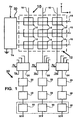
- Figure 1 schematically illustrates an MRAM device 10 including an array 12 of memory cells 14.
- the memory cells 14 are arranged in rows and columns of the array, with the rows extending along an x-direction and the columns extending along a y-direction. Only a relatively small number of memory cells 12 are shown in Figure 1 in order to simplify the description of the invention. In practice, arrays of any size may be used.
- Conductive traces functioning as word lines 16 extend along the x-direction in a plane of the memory cell array 10.
- Other conductive traces functioning as bit lines 18 extend along the y-direction in a plane of the memory cell array 10. There may be one word line 16 for each row of the array 10 and one bit line 18 for each column of the array 10.
- Each memory cell 14 is located at a cross point of a corresponding word line 16 and bit line 18, hence the name "resistive cross point memory" cell array, or RXPtM.
- the memory cells 14 are not limited to any particular type of device.
- the memory cells 14 may be fabricated to utilize spin dependent tunneling ("SDT") junction devices.
- SDT spin dependent tunneling
- the resistance value of each of the memory cells 14 is dependent upon the value (i.e., 1 or 0) of a data bit stored in the particular cell.
- the RXPtM cell array 10 also includes a row decode circuit 20.
- the row decode circuit 20 may apply either a constant supply voltage Vs or a ground potential to selected ones of the word lines 16.
- the constant supply voltage Vs may be provided by an external circuit.
- the RXPtM cell array 10 further includes a sense amplifier circuit for sensing the resistance of selected memory cells 14 during sense operations, and a write circuit for orienting the magnetization of selected memory cells 14 during write operations.
- the sense amplifier circuit is indicated generally at 22.
- the write circuit is not shown in order to simplify the explanation of the present invention.
- the sense amplifier circuit 22 includes a plurality of steering circuits 24 and sense amplifiers 26. Also, this circuit 22 preferably includes an analog to digital converter, including an integrator, a comparator, and a pre-settable counter (which sub-components are not individually indicated on drawing Figure 1). Multiple bit lines 18 are connected to each steering circuit 24. Each steering circuit 24 includes a set of switches that connect each bit line 18 to either a source of operating potential or to a sense amplifier 26. An output of the sense amplifier 26 is supplied to a data register 28, which, in turn, is coupled via an I/O controller circuit 30 to an output (indicated by arrowed numeral 32) of the MRAM device 10.
- the I/O controller 30 controls the entire MRAM device 10 (hence, the dashed box encompassing subparts of I/O controller 30 in Figure 1, to be further described below), and the outputs 32 may be common to one another (i.e., via a shared data I/O port, for example).
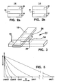
- a typical SDT junction memory cell 14 includes a magnetic layer 34 of "pinned” or fixed magnetic orientation.
- the layer 34 has a magnetization that is oriented in the plane of the pinned layer 34, and which is fixed in a selected direction in this plane so as not to change orientation in the presence of an applied magnetic field having a magnitude within a range of interest.
- the SDT junction device 14 also includes a "free" layer 36 having an orientation of magnetization that is not pinned. Rather, the magnetization of the layer 36 can be selectively oriented in either of two directions both lying in the plane of the layer 36.
- the orientation is said to be "parallel" (again, as is indicated by the arrows in Figure 2a). If the magnetization of the free and pinned 34 and 36 layers are generally in opposite directions (viewing Figure 2b), then the orientation is said to be "anti-parallel.”
- the magnetization in the free layer 36 may be selectively oriented by applying write currents to word and bit lines 16 and 18 that cross the memory cell 14.
- the free and pinned layers 34 and 36 are separated by an insulating tunnel barrier 38.
- the insulating tunnel barrier 38 allows quantum mechanical tunneling to occur between the free and pinned layers 34 and 36. This tunneling phenomenon is electron spin dependent, making the resistance of the SDT junction device 14 a function of the relative orientations of the magnetization of the free and pinned layers 34 and 36. Again, the resistance of a SDT junction device 14 will have a first value R if the orientation of magnetization of the free and pinned layers 34 and 36 is parallel, and will have a second value R+ ⁇ R if the magnetization of orientation is anti-parallel.
- a selected memory cell 14 is illustrated during a sense operation.
- the magnetization in the free layer 36 of the selected memory cell 14 was oriented by applying the currents to both the word line 16 and bit line 18 crossing that memory cell 14. Applying the currents to the word line 16 and bit line 18 caused the magnetization of the free layer 36 to rotate to a selected one of the parallel orientation or to the anti-parallel orientation.
- a resistance value i.e., R, or R+ ⁇ R
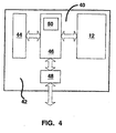
- FIG. 4 illustrates a MRAM memory chip 40 embodying the present invention.
- the MRAM chip includes a substrate 42 upon which the MRAM device 10 including the array 12 of cells is formed.
- a sense amplifier array 44 which includes a plurality of sense amplifiers 26, recalling the description of Figure 1 above.
- Controlling the interface of the array 44 of amplifiers 26, and the array of memory cells 12 is a global controller circuit 46.
- the global controller circuit 46 includes row circuits 20 and column circuits 22, and also moderates communication of data into and from the array 12 via an input/output port 48 (i.e., indicated with the doubleheaded arrow on Figure 4). While the global controller circuit 46 will include circuit portions in addition to those described here, it is important to note that this global controller circuit 46 includes a calibration controller 50.
- Calibration controller 50 is effective upon each command from global control circuit 46 to sense a data bit (i.e., to sense a relevant resistance value) from a memory cell of the memory cell array 12, to test the calibration of the one of the sense amplifiers of the amplifier array 44 which will effect this sensing of the selected memory cell.
- Figure 5 depicts a time versus voltage relationship that is preferably utilized according to the present invention in order to make a determination as to whether a particular sense amplifier has a correct calibration, and if not, to initiate a calibration of the particular sense amplifier.
- a particular time value is indicated as having a value of "1" and is labeled 1AVT (average time value).
- the time interval indicated as 1ATV is determined by individually testing (i.e., connecting) memory cells of a selected set of representative memory cells (i.e., representative of the cells of memory cell array 12) with an integrator circuit with the selected memory cell, and a pre-charged integration capacitor, an integrator, a comparator, and a pre-settable counter. The result is that the integration capacitor is discharged over time via the integrator, and the curve of voltage difference between Vdd and the charge level on the capacitance (i.e., in volts) is represented graphically.
- the time interval for each of the set of memory cells is determined, and the average value of time versus voltage is indicated graphically on the graph of Figure 5.
- the average value of time versus voltage is indicated on the graph of Figure 5 as 1AVT.
- values of 1 ⁇ 4 AVT, of 1 ⁇ 2 AVT, of 2AVT, and of 4AVT are determined.
- An outer pair of the time values indicated on Figure 5 i.e., the values of time indicated as 1 ⁇ 4 AVT and as 4AVT
- values of time indicative of "shorts" and "opens,” respectively are identified as values of time indicative of "shorts" and "opens," respectively. That is, if a particular memory cell is selected, and if the time interval measured is less that 1 ⁇ 4 AVT then the memory cell is considered to be shorted and to be bad. On the other hand, if the time interval measured is greater than 4AVT, then the memory cell is considered to be open-circuited, and is also bad. Bad memory cells are not used in testing for proper calibration of the sense amplifiers of the amplifier array 44.
- test limit values may be utilized.
- the selected and preferred values are powers of 2, and are easily implemented digitally. Further, these selected values for the test limits have been shown by actual testing of the invention to provide very reliable operation for the MRAM chip 40.
- Recal Hi/Lo recalibration high/recalibration low limit values.
- These Recal Hi/Lo values are the values within (i.e., between) which the time interval for a particular selected memory cell which is to be sensed must fall in order to indicate that the sense amplifier which will sense this memory cell has a proper calibration in view of the environmental factors then effective on the memory cell array 12. That is, the operating voltage Vdd of the MRAM chip 40 may have drifted, or the temperature of the memory cell array 12 may have changed so that the resistance of the memory cells and other circuit elements of the chip 40 is changed.
- the memory cell will be sensed, it is anticipated that the sensing result may be relied upon, and a recalibration of the sense amplifiers of array 44 will not be initiated.
- the time interval for the selected memory cell does not fall in the range from 1 ⁇ 2 AVT to 2AVT, but instead falls into one of the two "recalibrate" time interval ranges from 1 ⁇ 4 AVT to 1 ⁇ 2 AVT, or from 2AVT to 4AVT, then the sense amplifiers for array 44 are recalibrated.
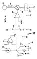
- circuit portion 52 of the calibration controller 50 is illustrated.
- This circuit portion 52 may be termed an individual sense amplifier portion, and it is switched into connection with a particular memory cell at the same time as the sense amplifier 26 which will be then used to sense that memory cell and as that sense amplifier is then calibrated (i.e., provided that the result of the calibration test explained above is to proceed without a calibration).
- the circuit portion 52 and sense amplifier 26 may share circuit elements, as will be clear in view of the explanation below.
- This circuit portion 52 includes a selected RXPtM cell 14, a capacitance 54 with a charging switch 54', a comparator amplifier 26', and a switching junction 56 receiving clock counts 58 from a source 60.
- junction 56 The conductivity of junction 56 (i.e., switched either opened or closed) is controlled by a voltage comparator circuit 62. Further, the number of clock pulses which pass through junction 56 while the junction 56 is switched closed is recorded in a counter 64 for data sensing and calibration uses, as will be further explained.
- Figure 6 Also included in the illustration of Figure 6 (which will be recalled to be a schematic circuit diagram) is an indication of the location and effect of a shorted memory cell (i.e., indicated with reference numeral 14'), and of an open memory cell (indicated with a reference numeral 14").
- the indications 14' and 14" seen on Figure 6 are provided merely so that the reader will have an appreciation of the location and effect of either a shorted or open memory cell. It will be understood in view of the above, and the following description, that a shorted or open resistive memory cell will be indicated in accord with the above description of the time values obtained for such shorted and open memory cells.
- the count value stored in counter 64 is indicative of a particular time interval as is graphically depicted on Figure 5, so that the time values 1 ⁇ 4 AVT, 1 ⁇ 2 AVT, 1AVT, 2AVT, and 4AVT are indicated according to a stored digital value in counter 64.
- a simple comparison of the digital value of actual clock counts stored in counter 64 to the counts for these time intervals determines whether a time value for the memory cell 14 under the then existing environmental factors for the MRAM chip 40, and with the existing calibration of sense amplifier 26 is acceptable according to the test explained above. If the time value is acceptable, then the count value in counter 64 is stored for use as an indication (i.e., in view of a further test) of the binary value ("1" or "0") stored in the cell 14 being sensed.
- the circuit 52 includes a load model 66 for the resistive cross point memory cell.
- This load model may be considered to be typical (i.e., representative) of the particular resistive cross point memory cell being sensed. Again, this particular resistive cross point memory cell may be shorted, may be open, or may have a normal resistance. However, if the resistive cross memory cell being sensed has a normal resistance, then the sense amplifier 26 may have an acceptable calibration, or may require recalibration before the sensing operation is completed.
- the comparator amplifier 26' is a constant voltage pre-amplifier (indicated generally with numeral 68), which effectively isolates the resistance R (i.e., resistance 14) from the integrator circuit 70.
- the comparator amplifier 26' behaves as a current source while maintaining a constant voltage across the resistance 14 of the resistive cross point memory cell being sensed.
- An integrator 70 includes the switch 54', the capacitor 54, and a ground connection (as indicated on the drawing Figure 6). This integrator allows the load current (i.e., sneak path current plus current through the load resistor R (i.e., resistor 14)) to discharge capacitor 54.
- the rate of decay of the voltage at the integrator is a direct function of the load current. If the load is shorted (i.e. 14') then the pre-amp current will be very high and the integrator will discharge very quickly. If the load is open (i.e., 14"), then the integrator 70 will discharge at a rate determined by the sneak path currents and by the circuit design. Then the discharge time will be very large.
- a normally resistive cross point memory cell i.e., resistance 14
- Comparator section 72 includes the comparator circuit 62, and a connection to a reference voltage source (indicated on Figure 6).
- the comparator 62 controls the gate 56 to open (i.e., switch closure) at the beginning of the integration period, and to close (i.e., switch opening) at the time when the voltage from capacitor 54 equals Vref.
- the circuit 52 also includes the counter and storage circuit 74, which includes switching junction 56, a connection to a clock pulse source (indicated at 60) and the counter 64.
- the result of the stored count value at counter 64 is compared to the reference values (i.e., 1 ⁇ 4 AVT, 1 ⁇ 2 AVT, 1AVT, 2AVT, and 4AVT) as described above, in order to determine if recalibration of the sense amplifier 26 is or is not necessary.
- the circuit 52 includes a representation at 76 of a current source, providing a current (which is a parasitic current) also flowing through the resistance of cell 14.
- the current source 76 is representative of sneak path currents resulting through the other resistive cells of a cell array, and realized at a particular cell 14 under evaluation.
- the cell is further sensed by writing either a zero ("0") or one ("1") value to the cell, and sensing its resistance value with the same calibration of sense amplifier 26; then the other of a zero ("0") or one (“1") value is written in the cell 14, and is sensed again with the same calibration of sense amplifier 26.
- each of these sensing steps gives a count value in counter 64, which is sensed and stored.
- a comparison between the first sensing count and the second sensing count; and between the first sensing count and the third sensing count, will give an unambiguous indication of which value of value (i.e., zero ("0") or one ("1")) was originally stored in the particular memory cell 14.
- This determined value of zero ("0") or one ("1") is then written back into cell 14 to complete the sense process for the particular memory cell 14.
- the above sensing process includes triple sensing steps each alternating with triple writing steps. Further, in the event that recalibration of the sense amplifier is necessary, this necessity is determined at the first sensing step before the first writing step, and the sense amplifier is then recalibrated. After this recalibration, the triple sense and triple write operation is carried out.
Landscapes
- Engineering & Computer Science (AREA)
- Computer Hardware Design (AREA)
- For Increasing The Reliability Of Semiconductor Memories (AREA)
- Mram Or Spin Memory Techniques (AREA)
- Hall/Mr Elements (AREA)
- Semiconductor Memories (AREA)
Applications Claiming Priority (2)
| Application Number | Priority Date | Filing Date | Title |
|---|---|---|---|
| US855118 | 1986-04-22 | ||
| US09/855,118 US6504779B2 (en) | 2001-05-14 | 2001-05-14 | Resistive cross point memory with on-chip sense amplifier calibration method and apparatus |
Publications (2)
| Publication Number | Publication Date |
|---|---|
| EP1260988A2 true EP1260988A2 (de) | 2002-11-27 |
| EP1260988A3 EP1260988A3 (de) | 2004-08-18 |
Family
ID=25320397
Family Applications (1)
| Application Number | Title | Priority Date | Filing Date |
|---|---|---|---|
| EP02253365A Withdrawn EP1260988A3 (de) | 2001-05-14 | 2002-05-14 | Widerstands-Kreuzpunkt-Speicherbauelement mit Kalibriersteuereinheit für einen Abtastverstärker |
Country Status (4)
| Country | Link |
|---|---|
| US (1) | US6504779B2 (de) |
| EP (1) | EP1260988A3 (de) |
| JP (1) | JP4067868B2 (de) |
| CN (1) | CN100474439C (de) |
Cited By (2)
| Publication number | Priority date | Publication date | Assignee | Title |
|---|---|---|---|---|
| EP1526549A1 (de) * | 2003-10-03 | 2005-04-27 | Hewlett-Packard Development Company, L.P. | Anordnung und Verfahren zur Kalibrierung einer Leseschaltung eines magnetischen Speichers |
| GB2380572B (en) * | 2001-07-25 | 2005-05-18 | Hewlett Packard Co | Fault tolerant magnetoresistive solid-state storage device |
Families Citing this family (28)
| Publication number | Priority date | Publication date | Assignee | Title |
|---|---|---|---|---|
| US6831854B2 (en) * | 2002-08-02 | 2004-12-14 | Unity Semiconductor Corporation | Cross point memory array using distinct voltages |
| US6804145B2 (en) * | 2002-11-01 | 2004-10-12 | Hewlett-Packard Development Company, L.P. | Memory cell sensing system and method |
| US6868025B2 (en) * | 2003-03-10 | 2005-03-15 | Sharp Laboratories Of America, Inc. | Temperature compensated RRAM circuit |
| US6873543B2 (en) * | 2003-05-30 | 2005-03-29 | Hewlett-Packard Development Company, L.P. | Memory device |
| US6898134B2 (en) * | 2003-07-18 | 2005-05-24 | Hewlett-Packard Development Company, L.P. | Systems and methods for sensing a memory element |
| US7006388B2 (en) * | 2003-08-28 | 2006-02-28 | Hewlett-Packard Development Company, L.P. | Memory with reference-initiated sequential sensing |
| US6990030B2 (en) * | 2003-10-21 | 2006-01-24 | Hewlett-Packard Development Company, L.P. | Magnetic memory having a calibration system |
| KR100988087B1 (ko) | 2003-11-24 | 2010-10-18 | 삼성전자주식회사 | Mram 특성 분석 장치 및 그 분석 방법 |
| US6999366B2 (en) * | 2003-12-03 | 2006-02-14 | Hewlett-Packard Development Company, Lp. | Magnetic memory including a sense result category between logic states |
| US7400670B2 (en) | 2004-01-28 | 2008-07-15 | Rambus, Inc. | Periodic calibration for communication channels by drift tracking |
| US7130235B2 (en) * | 2004-09-03 | 2006-10-31 | Hewlett-Packard Development Company, L.P. | Method and apparatus for a sense amplifier |
| US7239537B2 (en) * | 2005-01-12 | 2007-07-03 | International Business Machines Corporation | Method and apparatus for current sense amplifier calibration in MRAM devices |
| US7390616B2 (en) * | 2005-01-12 | 2008-06-24 | International Business Machines Corporation | Method for post lithographic critical dimension shrinking using post overcoat planarization |
| US7646625B2 (en) * | 2007-06-29 | 2010-01-12 | Qimonda Ag | Conditioning operations for memory cells |
| US20090103350A1 (en) * | 2007-10-18 | 2009-04-23 | Michael Kund | Method of Testing an Integrated Circuit, Method of Manufacturing an Integrated Circuit, and Integrated Circuit |
| KR20100087310A (ko) * | 2007-11-01 | 2010-08-04 | 프리스케일 세미컨덕터, 인크. | Mram 테스팅 |
| KR20140063821A (ko) | 2011-10-12 | 2014-05-27 | 휴렛-팩커드 디벨롭먼트 컴퍼니, 엘.피. | 교차점 메모리 구조를 위한 선택 디바이스 |
| CN103366791B (zh) * | 2012-03-30 | 2017-04-12 | 硅存储技术公司 | 即时可调整读出放大器 |
| KR20140035558A (ko) | 2012-09-14 | 2014-03-24 | 삼성전자주식회사 | 가변 저항 메모리 장치 및 그 동작 방법 |
| US9025367B1 (en) * | 2013-11-26 | 2015-05-05 | Realtek Semiconductor Corp. | Method and apparatus for sensing tunnel magneto-resistance |
| WO2016018404A1 (en) * | 2014-07-31 | 2016-02-04 | Hewlett-Packard Development Company, L.P. | Determining a resistance state of a cell in a crossbar memory array |
| US10056145B2 (en) * | 2016-03-02 | 2018-08-21 | Infineon Technologies Ag | Resistive memory transition monitoring |
| CN107154272B (zh) * | 2016-03-03 | 2020-07-03 | 东芝存储器株式会社 | 电流检测电路 |
| US10170162B2 (en) * | 2017-05-23 | 2019-01-01 | Sandisk Technologies Llc | Sense amplifier calibration |
| JP2020161201A (ja) * | 2019-03-27 | 2020-10-01 | キオクシア株式会社 | 半導体記憶装置 |
| CN112447257B (zh) * | 2019-08-30 | 2022-10-14 | 中电海康集团有限公司 | 测试结构和测试方法 |
| CN115188401B (zh) * | 2021-04-07 | 2025-10-14 | 浙江驰拓科技有限公司 | 保护mram数据的装置 |
| CN116466284A (zh) * | 2023-04-11 | 2023-07-21 | 上海壁仞智能科技有限公司 | 用于校准电阻的方法、设备、介质和系统 |
Family Cites Families (4)
| Publication number | Priority date | Publication date | Assignee | Title |
|---|---|---|---|---|
| JPH10162585A (ja) * | 1996-12-03 | 1998-06-19 | Sony Corp | トリミング機能付きセンスアンプを備えた半導体メモリ素子 |
| US6262625B1 (en) * | 1999-10-29 | 2001-07-17 | Hewlett-Packard Co | Operational amplifier with digital offset calibration |
| US6259644B1 (en) * | 1997-11-20 | 2001-07-10 | Hewlett-Packard Co | Equipotential sense methods for resistive cross point memory cell arrays |
| US6188615B1 (en) * | 1999-10-29 | 2001-02-13 | Hewlett-Packard Company | MRAM device including digital sense amplifiers |
-
2001
- 2001-05-14 US US09/855,118 patent/US6504779B2/en not_active Expired - Lifetime
-
2002
- 2002-05-08 JP JP2002132918A patent/JP4067868B2/ja not_active Expired - Fee Related
- 2002-05-14 CN CNB021193819A patent/CN100474439C/zh not_active Expired - Lifetime
- 2002-05-14 EP EP02253365A patent/EP1260988A3/de not_active Withdrawn
Cited By (2)
| Publication number | Priority date | Publication date | Assignee | Title |
|---|---|---|---|---|
| GB2380572B (en) * | 2001-07-25 | 2005-05-18 | Hewlett Packard Co | Fault tolerant magnetoresistive solid-state storage device |
| EP1526549A1 (de) * | 2003-10-03 | 2005-04-27 | Hewlett-Packard Development Company, L.P. | Anordnung und Verfahren zur Kalibrierung einer Leseschaltung eines magnetischen Speichers |
Also Published As
| Publication number | Publication date |
|---|---|
| CN100474439C (zh) | 2009-04-01 |
| CN1385859A (zh) | 2002-12-18 |
| JP4067868B2 (ja) | 2008-03-26 |
| JP2003022668A (ja) | 2003-01-24 |
| EP1260988A3 (de) | 2004-08-18 |
| US6504779B2 (en) | 2003-01-07 |
| US20020167838A1 (en) | 2002-11-14 |
Similar Documents
| Publication | Publication Date | Title |
|---|---|---|
| US6504779B2 (en) | Resistive cross point memory with on-chip sense amplifier calibration method and apparatus | |
| US6128239A (en) | MRAM device including analog sense amplifiers | |
| US6891768B2 (en) | Power-saving reading of magnetic memory devices | |
| US6999366B2 (en) | Magnetic memory including a sense result category between logic states | |
| US6765834B2 (en) | System and method for sensing memory cells of an array of memory cells | |
| US6791865B2 (en) | Memory device capable of calibration and calibration methods therefor | |
| US6259644B1 (en) | Equipotential sense methods for resistive cross point memory cell arrays | |
| US6674679B1 (en) | Adjustable current mode differential amplifier for multiple bias point sensing of MRAM having equi-potential isolation | |
| US6590804B1 (en) | Adjustable current mode differential amplifier | |
| US6625076B2 (en) | Circuit configuration fir evaluating the information content of a memory cell | |
| EP1096501B1 (de) | MRAM mit Leseverstärkern | |
| KR100890612B1 (ko) | 감지 증폭기 및 데이터 판독 방법 | |
| KR20020018149A (ko) | 정보 저장 장치 | |
| JP2003022668A5 (de) | ||
| US6898134B2 (en) | Systems and methods for sensing a memory element | |
| US6791873B1 (en) | Apparatus and method for generating a write current for a magnetic memory cell | |
| KR101054363B1 (ko) | 판독 동작 수행 방법 및 시스템 | |
| KR101136038B1 (ko) | 데이터 저장 디바이스, 메모리 셀 판독 동작 수행 방법 및시스템 | |
| KR101076371B1 (ko) | 데이터 저장 장치 및 판독 동작 수행 방법 | |
| US6826077B2 (en) | Magnetic random access memory with reduced parasitic currents | |
| US6804145B2 (en) | Memory cell sensing system and method |
Legal Events
| Date | Code | Title | Description |
|---|---|---|---|
| PUAI | Public reference made under article 153(3) epc to a published international application that has entered the european phase |
Free format text: ORIGINAL CODE: 0009012 |
|
| AK | Designated contracting states |
Kind code of ref document: A2 Designated state(s): AT BE CH CY DE DK ES FI FR GB GR IE IT LI LU MC NL PT SE TR |
|
| AX | Request for extension of the european patent |
Free format text: AL;LT;LV;MK;RO;SI |
|
| PUAL | Search report despatched |
Free format text: ORIGINAL CODE: 0009013 |
|
| AK | Designated contracting states |
Kind code of ref document: A3 Designated state(s): AT BE CH CY DE DK ES FI FR GB GR IE IT LI LU MC NL PT SE TR |
|
| AX | Request for extension of the european patent |
Extension state: AL LT LV MK RO SI |
|
| 17P | Request for examination filed |
Effective date: 20050215 |
|
| 17Q | First examination report despatched |
Effective date: 20050314 |
|
| AKX | Designation fees paid |
Designated state(s): DE GB |
|
| RBV | Designated contracting states (corrected) |
Designated state(s): DE GB |
|
| STAA | Information on the status of an ep patent application or granted ep patent |
Free format text: STATUS: THE APPLICATION IS DEEMED TO BE WITHDRAWN |
|
| 18D | Application deemed to be withdrawn |
Effective date: 20050927 |