EP1261029A2 - Halbleiteranordung und Herstellungsverfahren dafür - Google Patents
Halbleiteranordung und Herstellungsverfahren dafür Download PDFInfo
- Publication number
- EP1261029A2 EP1261029A2 EP02253531A EP02253531A EP1261029A2 EP 1261029 A2 EP1261029 A2 EP 1261029A2 EP 02253531 A EP02253531 A EP 02253531A EP 02253531 A EP02253531 A EP 02253531A EP 1261029 A2 EP1261029 A2 EP 1261029A2
- Authority
- EP
- European Patent Office
- Prior art keywords
- external connection
- semiconductor device
- connection terminals
- interconnection patterns
- wires
- Prior art date
- Legal status (The legal status is an assumption and is not a legal conclusion. Google has not performed a legal analysis and makes no representation as to the accuracy of the status listed.)
- Withdrawn
Links
Images





Classifications
-
- H—ELECTRICITY
- H10—SEMICONDUCTOR DEVICES; ELECTRIC SOLID-STATE DEVICES NOT OTHERWISE PROVIDED FOR
- H10W—GENERIC PACKAGES, INTERCONNECTIONS, CONNECTORS OR OTHER CONSTRUCTIONAL DETAILS OF DEVICES COVERED BY CLASS H10
- H10W72/00—Interconnections or connectors in packages
- H10W72/20—Bump connectors, e.g. solder bumps or copper pillars; Dummy bumps; Thermal bumps
-
- H—ELECTRICITY
- H10—SEMICONDUCTOR DEVICES; ELECTRIC SOLID-STATE DEVICES NOT OTHERWISE PROVIDED FOR
- H10W—GENERIC PACKAGES, INTERCONNECTIONS, CONNECTORS OR OTHER CONSTRUCTIONAL DETAILS OF DEVICES COVERED BY CLASS H10
- H10W72/00—Interconnections or connectors in packages
- H10W72/071—Connecting or disconnecting
-
- H—ELECTRICITY
- H10—SEMICONDUCTOR DEVICES; ELECTRIC SOLID-STATE DEVICES NOT OTHERWISE PROVIDED FOR
- H10W—GENERIC PACKAGES, INTERCONNECTIONS, CONNECTORS OR OTHER CONSTRUCTIONAL DETAILS OF DEVICES COVERED BY CLASS H10
- H10W74/00—Encapsulations, e.g. protective coatings
- H10W74/10—Encapsulations, e.g. protective coatings characterised by their shape or disposition
- H10W74/111—Encapsulations, e.g. protective coatings characterised by their shape or disposition the semiconductor body being completely enclosed
- H10W74/129—Encapsulations, e.g. protective coatings characterised by their shape or disposition the semiconductor body being completely enclosed forming a chip-scale package [CSP]
-
- H—ELECTRICITY
- H10—SEMICONDUCTOR DEVICES; ELECTRIC SOLID-STATE DEVICES NOT OTHERWISE PROVIDED FOR
- H10W—GENERIC PACKAGES, INTERCONNECTIONS, CONNECTORS OR OTHER CONSTRUCTIONAL DETAILS OF DEVICES COVERED BY CLASS H10
- H10W70/00—Package substrates; Interposers; Redistribution layers [RDL]
- H10W70/01—Manufacture or treatment
- H10W70/05—Manufacture or treatment of insulating or insulated package substrates, or of interposers, or of redistribution layers
-
- H—ELECTRICITY
- H10—SEMICONDUCTOR DEVICES; ELECTRIC SOLID-STATE DEVICES NOT OTHERWISE PROVIDED FOR
- H10W—GENERIC PACKAGES, INTERCONNECTIONS, CONNECTORS OR OTHER CONSTRUCTIONAL DETAILS OF DEVICES COVERED BY CLASS H10
- H10W70/00—Package substrates; Interposers; Redistribution layers [RDL]
- H10W70/60—Insulating or insulated package substrates; Interposers; Redistribution layers
- H10W70/62—Insulating or insulated package substrates; Interposers; Redistribution layers characterised by their interconnections
- H10W70/65—Shapes or dispositions of interconnections
- H10W70/654—Top-view layouts
- H10W70/656—Fan-in layouts
-
- H—ELECTRICITY
- H10—SEMICONDUCTOR DEVICES; ELECTRIC SOLID-STATE DEVICES NOT OTHERWISE PROVIDED FOR
- H10W—GENERIC PACKAGES, INTERCONNECTIONS, CONNECTORS OR OTHER CONSTRUCTIONAL DETAILS OF DEVICES COVERED BY CLASS H10
- H10W72/00—Interconnections or connectors in packages
- H10W72/01—Manufacture or treatment
- H10W72/012—Manufacture or treatment of bump connectors, dummy bumps or thermal bumps
- H10W72/01215—Manufacture or treatment of bump connectors, dummy bumps or thermal bumps forming coatings
-
- H—ELECTRICITY
- H10—SEMICONDUCTOR DEVICES; ELECTRIC SOLID-STATE DEVICES NOT OTHERWISE PROVIDED FOR
- H10W—GENERIC PACKAGES, INTERCONNECTIONS, CONNECTORS OR OTHER CONSTRUCTIONAL DETAILS OF DEVICES COVERED BY CLASS H10
- H10W72/00—Interconnections or connectors in packages
- H10W72/01—Manufacture or treatment
- H10W72/012—Manufacture or treatment of bump connectors, dummy bumps or thermal bumps
- H10W72/01221—Manufacture or treatment of bump connectors, dummy bumps or thermal bumps using local deposition
- H10W72/01225—Manufacture or treatment of bump connectors, dummy bumps or thermal bumps using local deposition in solid form, e.g. by using a powder or by stud bumping
-
- H—ELECTRICITY
- H10—SEMICONDUCTOR DEVICES; ELECTRIC SOLID-STATE DEVICES NOT OTHERWISE PROVIDED FOR
- H10W—GENERIC PACKAGES, INTERCONNECTIONS, CONNECTORS OR OTHER CONSTRUCTIONAL DETAILS OF DEVICES COVERED BY CLASS H10
- H10W72/00—Interconnections or connectors in packages
- H10W72/071—Connecting or disconnecting
- H10W72/072—Connecting or disconnecting of bump connectors
-
- H—ELECTRICITY
- H10—SEMICONDUCTOR DEVICES; ELECTRIC SOLID-STATE DEVICES NOT OTHERWISE PROVIDED FOR
- H10W—GENERIC PACKAGES, INTERCONNECTIONS, CONNECTORS OR OTHER CONSTRUCTIONAL DETAILS OF DEVICES COVERED BY CLASS H10
- H10W72/00—Interconnections or connectors in packages
- H10W72/071—Connecting or disconnecting
- H10W72/072—Connecting or disconnecting of bump connectors
- H10W72/07231—Techniques
- H10W72/07236—Soldering or alloying
-
- H—ELECTRICITY
- H10—SEMICONDUCTOR DEVICES; ELECTRIC SOLID-STATE DEVICES NOT OTHERWISE PROVIDED FOR
- H10W—GENERIC PACKAGES, INTERCONNECTIONS, CONNECTORS OR OTHER CONSTRUCTIONAL DETAILS OF DEVICES COVERED BY CLASS H10
- H10W72/00—Interconnections or connectors in packages
- H10W72/20—Bump connectors, e.g. solder bumps or copper pillars; Dummy bumps; Thermal bumps
- H10W72/221—Structures or relative sizes
-
- H—ELECTRICITY
- H10—SEMICONDUCTOR DEVICES; ELECTRIC SOLID-STATE DEVICES NOT OTHERWISE PROVIDED FOR
- H10W—GENERIC PACKAGES, INTERCONNECTIONS, CONNECTORS OR OTHER CONSTRUCTIONAL DETAILS OF DEVICES COVERED BY CLASS H10
- H10W72/00—Interconnections or connectors in packages
- H10W72/20—Bump connectors, e.g. solder bumps or copper pillars; Dummy bumps; Thermal bumps
- H10W72/221—Structures or relative sizes
- H10W72/222—Multilayered bumps, e.g. a coating on top and side surfaces of a bump core
- H10W72/223—Multilayered bumps, e.g. a coating on top and side surfaces of a bump core characterised by the structure of the outermost layers, e.g. multilayered coatings
-
- H—ELECTRICITY
- H10—SEMICONDUCTOR DEVICES; ELECTRIC SOLID-STATE DEVICES NOT OTHERWISE PROVIDED FOR
- H10W—GENERIC PACKAGES, INTERCONNECTIONS, CONNECTORS OR OTHER CONSTRUCTIONAL DETAILS OF DEVICES COVERED BY CLASS H10
- H10W72/00—Interconnections or connectors in packages
- H10W72/20—Bump connectors, e.g. solder bumps or copper pillars; Dummy bumps; Thermal bumps
- H10W72/241—Dispositions, e.g. layouts
- H10W72/242—Dispositions, e.g. layouts relative to the surface, e.g. recessed, protruding
-
- H—ELECTRICITY
- H10—SEMICONDUCTOR DEVICES; ELECTRIC SOLID-STATE DEVICES NOT OTHERWISE PROVIDED FOR
- H10W—GENERIC PACKAGES, INTERCONNECTIONS, CONNECTORS OR OTHER CONSTRUCTIONAL DETAILS OF DEVICES COVERED BY CLASS H10
- H10W72/00—Interconnections or connectors in packages
- H10W72/20—Bump connectors, e.g. solder bumps or copper pillars; Dummy bumps; Thermal bumps
- H10W72/241—Dispositions, e.g. layouts
- H10W72/244—Dispositions, e.g. layouts relative to underlying supporting features, e.g. bond pads, RDLs or vias
-
- H—ELECTRICITY
- H10—SEMICONDUCTOR DEVICES; ELECTRIC SOLID-STATE DEVICES NOT OTHERWISE PROVIDED FOR
- H10W—GENERIC PACKAGES, INTERCONNECTIONS, CONNECTORS OR OTHER CONSTRUCTIONAL DETAILS OF DEVICES COVERED BY CLASS H10
- H10W72/00—Interconnections or connectors in packages
- H10W72/20—Bump connectors, e.g. solder bumps or copper pillars; Dummy bumps; Thermal bumps
- H10W72/241—Dispositions, e.g. layouts
- H10W72/245—Dispositions, e.g. layouts of outermost layers of multilayered bumps, e.g. bump coating being only on a part of a bump core
-
- H—ELECTRICITY
- H10—SEMICONDUCTOR DEVICES; ELECTRIC SOLID-STATE DEVICES NOT OTHERWISE PROVIDED FOR
- H10W—GENERIC PACKAGES, INTERCONNECTIONS, CONNECTORS OR OTHER CONSTRUCTIONAL DETAILS OF DEVICES COVERED BY CLASS H10
- H10W72/00—Interconnections or connectors in packages
- H10W72/20—Bump connectors, e.g. solder bumps or copper pillars; Dummy bumps; Thermal bumps
- H10W72/251—Materials
- H10W72/252—Materials comprising solid metals or solid metalloids, e.g. PbSn, Ag or Cu
-
- H—ELECTRICITY
- H10—SEMICONDUCTOR DEVICES; ELECTRIC SOLID-STATE DEVICES NOT OTHERWISE PROVIDED FOR
- H10W—GENERIC PACKAGES, INTERCONNECTIONS, CONNECTORS OR OTHER CONSTRUCTIONAL DETAILS OF DEVICES COVERED BY CLASS H10
- H10W72/00—Interconnections or connectors in packages
- H10W72/20—Bump connectors, e.g. solder bumps or copper pillars; Dummy bumps; Thermal bumps
- H10W72/251—Materials
- H10W72/255—Materials of outermost layers of multilayered bumps, e.g. material of a coating
-
- H—ELECTRICITY
- H10—SEMICONDUCTOR DEVICES; ELECTRIC SOLID-STATE DEVICES NOT OTHERWISE PROVIDED FOR
- H10W—GENERIC PACKAGES, INTERCONNECTIONS, CONNECTORS OR OTHER CONSTRUCTIONAL DETAILS OF DEVICES COVERED BY CLASS H10
- H10W72/00—Interconnections or connectors in packages
- H10W72/20—Bump connectors, e.g. solder bumps or copper pillars; Dummy bumps; Thermal bumps
- H10W72/29—Bond pads specially adapted therefor
-
- H—ELECTRICITY
- H10—SEMICONDUCTOR DEVICES; ELECTRIC SOLID-STATE DEVICES NOT OTHERWISE PROVIDED FOR
- H10W—GENERIC PACKAGES, INTERCONNECTIONS, CONNECTORS OR OTHER CONSTRUCTIONAL DETAILS OF DEVICES COVERED BY CLASS H10
- H10W72/00—Interconnections or connectors in packages
- H10W72/50—Bond wires
- H10W72/551—Materials of bond wires
- H10W72/552—Materials of bond wires comprising metals or metalloids, e.g. silver
- H10W72/5522—Materials of bond wires comprising metals or metalloids, e.g. silver comprising gold [Au]
-
- H—ELECTRICITY
- H10—SEMICONDUCTOR DEVICES; ELECTRIC SOLID-STATE DEVICES NOT OTHERWISE PROVIDED FOR
- H10W—GENERIC PACKAGES, INTERCONNECTIONS, CONNECTORS OR OTHER CONSTRUCTIONAL DETAILS OF DEVICES COVERED BY CLASS H10
- H10W72/00—Interconnections or connectors in packages
- H10W72/90—Bond pads, in general
- H10W72/921—Structures or relative sizes of bond pads
- H10W72/922—Bond pads being integral with underlying chip-level interconnections
-
- H—ELECTRICITY
- H10—SEMICONDUCTOR DEVICES; ELECTRIC SOLID-STATE DEVICES NOT OTHERWISE PROVIDED FOR
- H10W—GENERIC PACKAGES, INTERCONNECTIONS, CONNECTORS OR OTHER CONSTRUCTIONAL DETAILS OF DEVICES COVERED BY CLASS H10
- H10W72/00—Interconnections or connectors in packages
- H10W72/90—Bond pads, in general
- H10W72/921—Structures or relative sizes of bond pads
- H10W72/923—Bond pads having multiple stacked layers
-
- H—ELECTRICITY
- H10—SEMICONDUCTOR DEVICES; ELECTRIC SOLID-STATE DEVICES NOT OTHERWISE PROVIDED FOR
- H10W—GENERIC PACKAGES, INTERCONNECTIONS, CONNECTORS OR OTHER CONSTRUCTIONAL DETAILS OF DEVICES COVERED BY CLASS H10
- H10W72/00—Interconnections or connectors in packages
- H10W72/90—Bond pads, in general
- H10W72/941—Dispositions of bond pads
- H10W72/944—Dispositions of multiple bond pads
- H10W72/9445—Top-view layouts, e.g. mirror arrays
-
- H—ELECTRICITY
- H10—SEMICONDUCTOR DEVICES; ELECTRIC SOLID-STATE DEVICES NOT OTHERWISE PROVIDED FOR
- H10W—GENERIC PACKAGES, INTERCONNECTIONS, CONNECTORS OR OTHER CONSTRUCTIONAL DETAILS OF DEVICES COVERED BY CLASS H10
- H10W72/00—Interconnections or connectors in packages
- H10W72/90—Bond pads, in general
- H10W72/951—Materials of bond pads
- H10W72/952—Materials of bond pads comprising metals or metalloids, e.g. PbSn, Ag or Cu
-
- H—ELECTRICITY
- H10—SEMICONDUCTOR DEVICES; ELECTRIC SOLID-STATE DEVICES NOT OTHERWISE PROVIDED FOR
- H10W—GENERIC PACKAGES, INTERCONNECTIONS, CONNECTORS OR OTHER CONSTRUCTIONAL DETAILS OF DEVICES COVERED BY CLASS H10
- H10W90/00—Package configurations
- H10W90/701—Package configurations characterised by the relative positions of pads or connectors relative to package parts
- H10W90/721—Package configurations characterised by the relative positions of pads or connectors relative to package parts of bump connectors
- H10W90/724—Package configurations characterised by the relative positions of pads or connectors relative to package parts of bump connectors between a chip and a stacked insulating package substrate, interposer or RDL
Definitions
- the present invention relates to a semiconductor device and a method of production of the same, more particularly relates to a semiconductor device produced by forming external connection terminals on an electrode formation surface of a semiconductor wafer and a method of production of the same.
- FIGS. 12A to 12I show a method of production of a semiconductor device formed with metal posts as external connection terminals on an electrode formation surface of a semiconductor wafer.
- a passivation film 14 FIG. 12A
- a conductive layer 16 by sputtering
- FIG. 12C the surface of the conductive layer 16 is covered by a photosensitive resist 18
- FIG. 12D the photosensitive resist 18 is exposed and developed to expose portions for forming interconnection patterns at the surface of the conductive layer 16.
- the electrodes 12 are arranged at an extremely high density at for example the periphery of the electrode formation surface of the semiconductor wafer 10.
- the interconnection patterns 20 are formed by electroplating the exposed surfaces of the conductive layer 16 by copper.
- the interconnection patterns 20 are formed led out from the electrodes 12 so as to secure spaces for arrangement of the external connection terminals.
- the photosensitive resist 18 is removed and the surfaces of the interconnection patterns 20 and conductive layer 16 are covered by a dry film 22 (FIG. 12F),
- This dry film 22 is for forming the copper posts 24 forming the external connection terminals (FIG. 12G).
- the dry film 22 is exposed and developed to form holes for plating at portions for forming the copper posts 24 on the interconnection patterns 20. By electroplating these portions by copper, copper is built up in the plating holes and metal posts 24 of heights of about 100 ⁇ m are formed.
- the surfaces of the copper posts 24 are successively plated by nickel, palladium, etc. to form the barrier layers 26.
- the dry film 22 is removed, then the portions of the conductive layer 16 exposed at the electrode formation surface are removed by etching (FIG. 12H). In this way, the electrode formation surface of the semiconductor wafer 10 is formed with copper posts 24 electrically connected with the electrodes 12 through the interconnection patterns 20.
- the electrode formation surface of the semiconductor wafer 10 is covered with a resin 28 for sealing.
- the resin 28 is formed to substantially the same thickness as the copper posts 24.
- the end faces of the copper posts 24 are exposed at the surface of the resin 28.
- solder balls are placed on the surfaces of the barrier layers 26 and the solder made to reflow to form solder bumps (not shown).
- the semiconductor wafer 10 can be diced along with the resin 28 to obtain chip-sized semiconductor devices.
- FIGS. 13A to 13I show another method for producing a chip-sized semiconductor device.
- the semiconductor device obtained by this method of production has gold wires bent in L-shapes for use as external connection terminals.
- the steps shown in FIGS. 13A to 13E are basically no different from the steps shown in the above FIGS. 12A to 12E.
- the interconnection patterns 20 are not sealed by resin.
- the interconnection patterns 20 are formed by gold plating so as to enable them to be left as they are exposed at the outside surface of the semiconductor device.
- the photosensitive resist 18 (FIG. 13E) is removed.
- the electrode formation surface is covered by a resist, then holes 30a are formed in the interconnection patterns 20 at portions for later bonding of the gold wires.
- the electrode formation surface is covered by the resist 30 so as to cover only the outer surfaces of the gold wires with reinforcement plating after bonding the gold wires.
- the gold wires are bonded to the interconnection patterns 20 in register with the openings 30a (FIG. 13G).
- the gold wires are bent into L-shapes and the ends thereof are cut off to form the external connection terminals 32.
- the outer surfaces of the gold wires are plated to reinforce the wires (the plating material is not shown in the drawing), then the resist 30 is removed and, as shown in FIG. 13I, the exposed portions of the conductive layer 16 are removed by etching.
- the electrode formation surface of the semiconductor wafer 10 is formed with external connection terminals 32 electrically connected with the electrodes 12 through the interconnection patterns 20.
- the semiconductor wafer 10 is diced to obtain semiconductor devices provided with external connection terminals 32 comprised of wires bent into L-shapes.
- the conductive layer 16 was formed on the passivation film 14, but it is also possible to cover the passivation film 14 by a polyimide film and form the conductive layer 16 on the surface of the polyimide film.
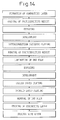
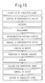
- Steps for producing a semiconductor device using the above copper posts as external connection terminals and steps for producing a semiconductor device using gold wires bent into L-shapes as external connection terminals are shown in FIGS. 14 and 15.
- the steps produce chip-sized semiconductor devices by processing the semiconductor wafer to form external connection terminals electrically connected to the electrode terminals formed on it, then dicing the semiconductor wafer.
- the methods of the prior art utilize complicated steps, so there are the problems that the production efficiency is reduced and the manufacturing costs increased.
- the present invention was made to solve the problems in the methods of production of the prior art for producing semiconductor devices by processing a semiconductor wafer.
- An object of the present invention is to provide a highly reliable semiconductor device able to be produced by a simpler method and thereby able to improve the production efficiency and able to arrange external connection terminals at a higher density and thereby able to handle a greater number of pins and a method of production of the same.
- a semiconductor device provided with semiconductor elements, such as transistors, formed on a semiconductor substrate, external connection terminals connecting these elements to an external circuit, and interconnection patterns connecting electrodes of the semiconductor elements to the external connection terminals, wherein the external connection terminals are formed by wires comprised of a conductive material and the parts of the wires bonded to the interconnection patterns are buried in the metal layer forming the interconnection patterns.
- the metal layer forming the interconnection patterns is preferably formed by copper plating, gold plating or the like.
- wires of the conductive material forming the external connection terminals it is preferable to use gold wires, copper wires, etc.
- the metal layer and the wires are fabricated by the same material. Therefore, preferably the metal layer is formed by gold plating and the wires are comprised of gold or the metal layer is formed by copper plating and the wires are comprised of copper.
- the external connection terminals can be covered by the material of the metal layer forming the interconnection patterns.
- the surface of the semiconductor device where the interconnection patterns are formed can be sealed so as to leave exposed the external connection terminals.
- a method of production of a semiconductor device provided with semiconductor elements formed on a semiconductor substrate, external connection terminals connecting the elements to an external circuit, and interconnection patterns connecting electrodes of the semiconductor elements to the external connection terminals, comprising the steps of forming a conductive layer on the entire surface of the semiconductor substrate where the electrodes are formed, forming a resist pattern on the surface of the conductive layer exposing the conductive layer at portions where pads to which the external connection terminals are to be connected and the interconnection patterns are to be formed, bonding wires comprised of a conductive material to the conductive layer at portions where the pads are to be formed to form external connection terminals, forming a metal layer at the exposed portions of the conductive layer, removing the resist, and removing the conductive layer exposed by the removal of the resist to form interconnection patterns.
- FIGS. 1A to 1I are views for explaining a method of production of a semiconductor device according to a first embodiment of the present invention.
- a conductive layer 16 is formed on the electrode formation surface of the semiconductor wafer 10 (FIG. 1B).
- a chromium layer is formed by sputtering, then a copper layer is formed by sputtering to obtain the conductive layer 16.
- the surface of the passivation film 14 may be formed with a polyimide or other electrical insulating layer (not shown) as a protective film, then the conductive layer 16 formed.
- a photosensitive resist 18 is coated on the entire electrode formation surface of the semiconductor wafer 10 to cover the surface of the conductive layer 16 by the photosensitive resist 18 (FIG. 1C).
- the photosensitive resist 18 is exposed and developed for patterning to, as shown in FIG. 1D, leave exposed only the portions for forming the interconnection patterns for rewiring on the surface of the conductive layer 16.
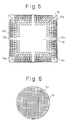
- FIG. 5 is a plan view of one chip section of the semiconductor wafer in the state with the photosensitive resist 18 exposed and developed.
- Reference numeral 18 indicates a photosensitive resist covering the electrode formation surface of the semiconductor wafer 10, 16a portions where the conductive layer 16 is left exposed in accordance with the arrangement of the interconnection patterns, 16b portions forming pads formed at the ends of the interconnection patterns, and 16c portions of base ends of the interconnection patterns connected to the electrodes 12.
- the method of production of a semiconductor device of the present embodiment is characterized by the formation of external connection terminals 50 by the method of bonding copper wires to portions 16b forming the pads after patterning the photosensitive resist 18 as shown in FIG. 1E.
- the tips of the copper wires are melted into ball shapes, the ball-shaped portions are bonded with the portions 16b forming the pads, then the wires are pulled up and cut, whereby external connection terminals 50 with projections 50a made of the wires projecting up from the ball-shaped portions are formed.
- external connection terminals 50 are formed at all of the portions 16b forming the pads formed on the electrode formation surface.
- the external connection terminals 50 are formed by wire bonding, the work is extremely efficient. Further, the external connection terminals 50 can be formed using conventional bonding tools. Further, since the tips of the copper wires are shaped into balls and bonded with the conductive layer 16 and then the copper wires are cut while being pulled up to form the external connection terminals 50, the operation of bending the wires to L-shapes as in the prior art is not required, the dimensions and shapes of the external connection terminals 50 are easily kept uniform, and the work can be performed efficiently.
- the exposed surfaces of the conductive layer 16 are electroplated with copper to form the interconnection patterns 52 as shown in FIG. 1F.
- the surfaces of the external connection terminals 50 are also covered by copper plating.
- the surfaces of the external connection terminals and the surfaces of the interconnection patterns 52 are plated to prevent diffusion of the solder at the time of mounting. In the present embodiment, they were successively plated with nickel, palladium, and gold.
- the photosensitive resist 18 (FIG. 1F) is removed from the electrode formation surface of the semiconductor wafer 10, then the exposed portions of the conductive layer 16 are etched away (FIG. 1H).
- the exposed portions of the conductive layer 16 can be removed without covering the interconnection patterns 52 by a resist etc. Due to this, the passivation film 14 is exposed and the interconnection patterns 52 become independent.
- the electrode formation surface of the semiconductor wafer 10 is sealed by a resin to seal the interconnection patterns 52 and the passivation film 14 by the resin 28 (FIG. 1I).
- a resin sealing step a transfer mold method using a sealing mold or a potting method is used. Due to the resin sealing step, a semiconductor wafer 10 with external connection terminals 50 projecting from a resin sealed surface is obtained.
- FIG. 6 shows the thus obtained semiconductor wafer 10. By dicing this, individual semiconductor devices 54 are obtained.
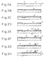
- FIGS. 2A to 2H are views for explaining a method of production of a semiconductor device according to a second embodiment of the present invention.
- the method of production of this embodiment is basically the same as the method of production of the above embodiment, but in this embodiment, after forming the interconnection patterns for rewiring on the electrode formation surface of the semiconductor wafer, the electrode formation surface is left as it is without sealing by a resin in the final product.
- a conductive layer 16 is formed.
- chromium, titanium-tungsten alloy, and gold are deposited in that order on the electrode formation surface by sputtering to form the conductive layer 16.
- a photosensitive resist 18 is coated on the surface of the conductive layer 16 (FIG. 2C), then the photosensitive resist 18 is exposed and developed for patterning (FIG. 2D) so as to expose the portions 16a (FIG. 5) later forming the interconnection patterns, portions 16b (FIG. 5) forming the pads, and portions 16c (FIG. 5) connecting with the electrodes 12 at the surface of the conductive layer 16.
- the exposed surfaces of the conductive layer 16 are electroplated with gold to form the interconnection patterns 62 as shown in FIG. 1F.
- the interconnection patterns 62 are formed by gold plating.
- gold plating as illustrated, the surfaces of the external connection terminals 60 are covered by gold plating as well.
- the photosensitive resist 18 (FIG. 2F) is removed from the electrode formation surface of the semiconductor wafer 10, then the exposed portions of the conductive layer 16 are etched away (FIG. 2H). Due to this, the passivation film 14 is exposed and the interconnection patterns become independent.
- the semiconductor device is obtained by dicing the semiconductor wafer into individual chips.
- the interconnection patterns 62 independent (after step explained at FIG. 2H)
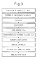
- FIG. 3 is a flow chart of the method of production of a semiconductor device according to the first embodiment of the present invention
- FIG. 4 is a flow chart of the method of production according to the second embodiment.
- FIGS. 7A and 7B and FIGS. 8A and 8B are enlarged sectional views of bonding portions of external connection terminals and interconnection patterns of semiconductor devices obtained by the method of production of a semiconductor device according to the present invention and methods of production of a semiconductor device of the prior art.
- FIGS. 7A and 7B show examples of semiconductor devices sealing the electrode formation surfaces with a resin after formation of the interconnection patterns, while FIGS. 8A and 8B show examples of semiconductor devices with interconnection patterns exposed.
- interconnection patterns 52 and 62 are formed by copper plating or gold plating.
- FIGS. 7B and 8B after the interconnection patterns 20 are formed, copper posts 24 or external connection terminals 32 made of gold wires are formed as external connection terminals on the surface of the interconnection patterns 20.
- the external connection terminals 50 and 60 are bonded to the conductive layer 16 and the base sides (bonding parts) of the external connection terminals 50 and 60 are buried in the copper plating layer or gold plating layer forming the interconnection patterns 52 and 62. Therefore, in the case of the semiconductor device according to the present invention, compared with that of the prior art, the height of the external connection terminals can be lowered by at least the amount of thickness of the interconnection patterns 52 and 62. Due to this, the method of production of a semiconductor device according to the present invention is effective in forming the semiconductor device thin and compact. Further, as clear from a comparison of FIG. 8A and FIG. 8B, in the case of the present invention, the overall height of the external connection terminals 60 becomes low. Due to this as well, according to the invention, the semiconductor device can be produced compactly as a whole.
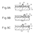
- FIGS. 9A to 9C show external connection terminals 60 formed by bonding gold wires to portions 16b of the conductive layer 16 forming pads and exposed at openings of a patterned resist 18.
- FIG. 9A shows the case where the opening of the resist 18 defining the portion 16b forming the pad is formed larger than the bonding part of the gold wire. In this case, the gold wire is merely bonded to the portion 16b at its bottom.
- FIG. 9B shows the case where the opening is formed somewhat smaller than the case of FIG. 9A. The gold wire is bonded to the portion 16b at its bottom. Part of the sides of the bonding part of the gold wire is in contact with the sides of the photosensitive resist 18.
- FIG. 9A shows the case where the opening of the resist 18 defining the portion 16b forming the pad is formed larger than the bonding part of the gold wire. In this case, the gold wire is merely bonded to the portion 16b at its bottom.
- FIG. 9B shows the case where the opening is formed somewhat smaller than the case of FIG. 9
- FIG. 9C shows the case where the opening is of a size approximately the same as the bonding part of the gold wire.
- the bottom of the gold wire is bonded to the portion 16b forming the pad.
- the sides of the bonding part of the gold wire are in overall contact with the sides of the photosensitive resist 18.
- the external connection terminals 50 and 60 are further reliably supported.
- FIGS. 10A and 10B and FIGS. 11A and 11B show comparisons of semiconductor devices of the present invention mounted on boards as opposed to semiconductor devices of the prior art mounted on boards.
- FIGS. 10A and 10B show a comparison of a semiconductor device according to the present invention (FIG. 10A) and a semiconductor device of the prior art using copper posts as external connection terminals (FIG. 10B).
- FIG. 10B when mounting a semiconductor device formed with copper posts 24 onto a board 40 by solder 42, only the barrier layers 26 formed at the end faces of the copper posts 24 are exposed at the surface of the resin 28 with its poor solder wettability. Therefore, the solder 42 sometimes does not form a meniscus suitable for bonding with the copper posts.
- the solder 42 when mounting the semiconductor device according to the present invention, as shown in FIG. 10A, due to the projections 50a projecting from the external connection terminals 50, the solder 42 forms a sufficient meniscus and therefore the device is reliably mounted to the board.
- FIGS. 11A and 11B show a comparison of a semiconductor device of the present invention with interconnection patterns exposed (FIG. 11A) and a semiconductor device of the prior art (FIG. 11B).
- FIG. 11B when mounting a semiconductor device of the prior art provided with external connection terminals 32 formed by bending gold wires into L-shapes onto a board 40, the tips of the external connection terminals 32 are brought into abutment with the board 40 for bonding and therefore the semiconductor device and the board 40 are spaced away from each other.
- solder 42 is deposited in a meniscus on projections 60a of the external connection terminals 60 and therefore the semiconductor device and board 40 are reliably bonded and, also, the distance between the semiconductor device and board 40 can be shortened.
- the semiconductor device according to the present invention can be reliably mounted to a board so as to guarantee a high reliability such as a good electrical connection with the board.
- the semiconductor device and method of production of the same of the present invention it is possible to easily form external connection terminals by bonding wires and thereby possible to simplify the steps for producing a semiconductor device. Further, according to the present invention, it is possible to improve the production efficiency of a semiconductor device and reduce the manufacturing costs of the semiconductor device.
- the present invention enables external connection terminals to be arranged at a high density and enables larger number of pins to be handled. Further, it is possible to provide a highly reliable semiconductor device where the external connection terminals are reliably bonded with the board.
Landscapes
- Internal Circuitry In Semiconductor Integrated Circuit Devices (AREA)
- Wire Bonding (AREA)
Applications Claiming Priority (2)
| Application Number | Priority Date | Filing Date | Title |
|---|---|---|---|
| JP2001157451A JP2002353371A (ja) | 2001-05-25 | 2001-05-25 | 半導体装置及びその製造方法 |
| JP2001157451 | 2001-05-25 |
Publications (2)
| Publication Number | Publication Date |
|---|---|
| EP1261029A2 true EP1261029A2 (de) | 2002-11-27 |
| EP1261029A3 EP1261029A3 (de) | 2004-06-09 |
Family
ID=19001308
Family Applications (1)
| Application Number | Title | Priority Date | Filing Date |
|---|---|---|---|
| EP02253531A Withdrawn EP1261029A3 (de) | 2001-05-25 | 2002-05-20 | Halbleiteranordung und Herstellungsverfahren dafür |
Country Status (5)
| Country | Link |
|---|---|
| US (1) | US6646357B2 (de) |
| EP (1) | EP1261029A3 (de) |
| JP (1) | JP2002353371A (de) |
| KR (1) | KR20020090301A (de) |
| TW (1) | TW544742B (de) |
Families Citing this family (3)
| Publication number | Priority date | Publication date | Assignee | Title |
|---|---|---|---|---|
| US7271497B2 (en) * | 2003-03-10 | 2007-09-18 | Fairchild Semiconductor Corporation | Dual metal stud bumping for flip chip applications |
| JP4863746B2 (ja) * | 2006-03-27 | 2012-01-25 | 富士通株式会社 | 半導体装置およびその製造方法 |
| DE102007046556A1 (de) * | 2007-09-28 | 2009-04-02 | Infineon Technologies Austria Ag | Halbleiterbauelement mit Kupfermetallisierungen |
Family Cites Families (5)
| Publication number | Priority date | Publication date | Assignee | Title |
|---|---|---|---|---|
| US5476211A (en) | 1993-11-16 | 1995-12-19 | Form Factor, Inc. | Method of manufacturing electrical contacts, using a sacrificial member |
| US5650667A (en) * | 1995-10-30 | 1997-07-22 | National Semiconductor Corporation | Process of forming conductive bumps on the electrodes of semiconductor chips using lapping and the bumps thereby created |
| AU8280398A (en) | 1997-06-30 | 1999-01-19 | Formfactor, Inc. | Sockets for semiconductor devices with spring contact elements |
| JP2000200804A (ja) * | 1998-10-30 | 2000-07-18 | Shinko Electric Ind Co Ltd | 半導体装置及びその製造方法 |
| JP3524441B2 (ja) * | 1999-08-10 | 2004-05-10 | 新光電気工業株式会社 | 配線形成方法 |
-
2001
- 2001-05-25 JP JP2001157451A patent/JP2002353371A/ja active Pending
-
2002
- 2002-05-20 EP EP02253531A patent/EP1261029A3/de not_active Withdrawn
- 2002-05-20 US US10/151,607 patent/US6646357B2/en not_active Expired - Lifetime
- 2002-05-20 KR KR1020020027903A patent/KR20020090301A/ko not_active Withdrawn
- 2002-05-21 TW TW091110671A patent/TW544742B/zh not_active IP Right Cessation
Also Published As
| Publication number | Publication date |
|---|---|
| TW544742B (en) | 2003-08-01 |
| JP2002353371A (ja) | 2002-12-06 |
| KR20020090301A (ko) | 2002-12-02 |
| EP1261029A3 (de) | 2004-06-09 |
| US6646357B2 (en) | 2003-11-11 |
| US20020175426A1 (en) | 2002-11-28 |
Similar Documents
| Publication | Publication Date | Title |
|---|---|---|
| KR100301357B1 (ko) | 반도체장치및그제조방법및리드프레임의제조방법 | |
| US6559528B2 (en) | Semiconductor device and method for the fabrication thereof | |
| US6703310B2 (en) | Semiconductor device and method of production of same | |
| KR100838440B1 (ko) | 전자 장치용 기판과 그 제조 방법, 및 전자 장치와 그 제조방법 | |
| US6818998B2 (en) | Stacked chip package having upper chip provided with trenches and method of manufacturing the same | |
| US6921980B2 (en) | Integrated semiconductor circuit including electronic component connected between different component connection portions | |
| US7670962B2 (en) | Substrate having stiffener fabrication method | |
| US6891273B2 (en) | Semiconductor package and fabrication method thereof | |
| EP1213756A2 (de) | Halbleitergehäuseherstellung und Halbleitergehäuse | |
| US20030230805A1 (en) | Semiconductor device and manufacturing method thereof | |
| US8945994B2 (en) | Single layer coreless substrate | |
| US6596560B1 (en) | Method of making wafer level packaging and chip structure | |
| US7705471B2 (en) | Conductive bump structure of circuit board and method for forming the same | |
| KR20070096016A (ko) | 본드 패드를 갖는 상호 결선 구조체 및 본드 패드 상의범프 사이트 형성 방법 | |
| US6465886B1 (en) | Semiconductor device having circuit pattern and lands thereon | |
| TWI413210B (zh) | 電子裝置封裝及製造方法 | |
| EP1109219A2 (de) | Halbleiteranordnung mit einer Verdrahtungsschicht | |
| US6525424B2 (en) | Semiconductor device and its manufacturing method | |
| US7202421B2 (en) | Electronic elements, method for manufacturing electronic elements, circuit substrates, method for manufacturing circuit substrates, electronic devices and method for manufacturing electronic devices | |
| EP1003209A1 (de) | Verfahren zur Herstellung eines Halbleiterbauelements | |
| JP2005057264A (ja) | パッケージ化された電気構造およびその製造方法 | |
| US6929971B2 (en) | Semiconductor device and its manufacturing method | |
| US6646357B2 (en) | Semiconductor device and method of production of same | |
| US6730539B2 (en) | Method of manufacturing semiconductor device package | |
| KR20080045017A (ko) | 금속 범프를 갖는 반도체 칩 패키지 및 그 제조방법 |
Legal Events
| Date | Code | Title | Description |
|---|---|---|---|
| PUAI | Public reference made under article 153(3) epc to a published international application that has entered the european phase |
Free format text: ORIGINAL CODE: 0009012 |
|
| AK | Designated contracting states |
Kind code of ref document: A2 Designated state(s): AT BE CH CY DE DK ES FI FR GB GR IE IT LI LU MC NL PT SE TR |
|
| AX | Request for extension of the european patent |
Free format text: AL;LT;LV;MK;RO;SI |
|
| PUAL | Search report despatched |
Free format text: ORIGINAL CODE: 0009013 |
|
| AK | Designated contracting states |
Kind code of ref document: A3 Designated state(s): AT BE CH CY DE DK ES FI FR GB GR IE IT LI LU MC NL PT SE TR |
|
| AX | Request for extension of the european patent |
Extension state: AL LT LV MK RO SI |
|
| RIC1 | Information provided on ipc code assigned before grant |
Ipc: 7H 01L 23/31 B Ipc: 7H 01L 21/60 B Ipc: 7H 01L 23/485 A |
|
| 17P | Request for examination filed |
Effective date: 20041129 |
|
| AKX | Designation fees paid |
Designated state(s): DE FR GB |
|
| 17Q | First examination report despatched |
Effective date: 20070220 |
|
| STAA | Information on the status of an ep patent application or granted ep patent |
Free format text: STATUS: THE APPLICATION IS DEEMED TO BE WITHDRAWN |
|
| 18D | Application deemed to be withdrawn |
Effective date: 20070703 |