EP1213756A2 - Halbleitergehäuseherstellung und Halbleitergehäuse - Google Patents
Halbleitergehäuseherstellung und Halbleitergehäuse Download PDFInfo
- Publication number
- EP1213756A2 EP1213756A2 EP02003794A EP02003794A EP1213756A2 EP 1213756 A2 EP1213756 A2 EP 1213756A2 EP 02003794 A EP02003794 A EP 02003794A EP 02003794 A EP02003794 A EP 02003794A EP 1213756 A2 EP1213756 A2 EP 1213756A2
- Authority
- EP
- European Patent Office
- Prior art keywords
- wiring
- semiconductor
- supporting member
- mounting
- substrate
- Prior art date
- Legal status (The legal status is an assumption and is not a legal conclusion. Google has not performed a legal analysis and makes no representation as to the accuracy of the status listed.)
- Withdrawn
Links
Images








Classifications
-
- H—ELECTRICITY
- H10—SEMICONDUCTOR DEVICES; ELECTRIC SOLID-STATE DEVICES NOT OTHERWISE PROVIDED FOR
- H10W—GENERIC PACKAGES, INTERCONNECTIONS, CONNECTORS OR OTHER CONSTRUCTIONAL DETAILS OF DEVICES COVERED BY CLASS H10
- H10W74/00—Encapsulations, e.g. protective coatings
- H10W74/01—Manufacture or treatment
- H10W74/019—Manufacture or treatment using temporary auxiliary substrates
-
- H—ELECTRICITY
- H10—SEMICONDUCTOR DEVICES; ELECTRIC SOLID-STATE DEVICES NOT OTHERWISE PROVIDED FOR
- H10W—GENERIC PACKAGES, INTERCONNECTIONS, CONNECTORS OR OTHER CONSTRUCTIONAL DETAILS OF DEVICES COVERED BY CLASS H10
- H10W70/00—Package substrates; Interposers; Redistribution layers [RDL]
- H10W70/60—Insulating or insulated package substrates; Interposers; Redistribution layers
-
- H—ELECTRICITY
- H05—ELECTRIC TECHNIQUES NOT OTHERWISE PROVIDED FOR
- H05K—PRINTED CIRCUITS; CASINGS OR CONSTRUCTIONAL DETAILS OF ELECTRIC APPARATUS; MANUFACTURE OF ASSEMBLAGES OF ELECTRICAL COMPONENTS
- H05K3/00—Apparatus or processes for manufacturing printed circuits
- H05K3/30—Assembling printed circuits with electric components, e.g. with resistors
-
- H—ELECTRICITY
- H10—SEMICONDUCTOR DEVICES; ELECTRIC SOLID-STATE DEVICES NOT OTHERWISE PROVIDED FOR
- H10W—GENERIC PACKAGES, INTERCONNECTIONS, CONNECTORS OR OTHER CONSTRUCTIONAL DETAILS OF DEVICES COVERED BY CLASS H10
- H10W70/00—Package substrates; Interposers; Redistribution layers [RDL]
- H10W70/60—Insulating or insulated package substrates; Interposers; Redistribution layers
- H10W70/67—Insulating or insulated package substrates; Interposers; Redistribution layers characterised by their insulating layers or insulating parts
- H10W70/688—Flexible insulating substrates
-
- H—ELECTRICITY
- H10—SEMICONDUCTOR DEVICES; ELECTRIC SOLID-STATE DEVICES NOT OTHERWISE PROVIDED FOR
- H10W—GENERIC PACKAGES, INTERCONNECTIONS, CONNECTORS OR OTHER CONSTRUCTIONAL DETAILS OF DEVICES COVERED BY CLASS H10
- H10W74/00—Encapsulations, e.g. protective coatings
- H10W74/01—Manufacture or treatment
-
- H—ELECTRICITY
- H10—SEMICONDUCTOR DEVICES; ELECTRIC SOLID-STATE DEVICES NOT OTHERWISE PROVIDED FOR
- H10W—GENERIC PACKAGES, INTERCONNECTIONS, CONNECTORS OR OTHER CONSTRUCTIONAL DETAILS OF DEVICES COVERED BY CLASS H10
- H10W74/00—Encapsulations, e.g. protective coatings
- H10W74/01—Manufacture or treatment
- H10W74/014—Manufacture or treatment using batch processing
-
- H—ELECTRICITY
- H10—SEMICONDUCTOR DEVICES; ELECTRIC SOLID-STATE DEVICES NOT OTHERWISE PROVIDED FOR
- H10W—GENERIC PACKAGES, INTERCONNECTIONS, CONNECTORS OR OTHER CONSTRUCTIONAL DETAILS OF DEVICES COVERED BY CLASS H10
- H10W74/00—Encapsulations, e.g. protective coatings
- H10W74/10—Encapsulations, e.g. protective coatings characterised by their shape or disposition
- H10W74/111—Encapsulations, e.g. protective coatings characterised by their shape or disposition the semiconductor body being completely enclosed
- H10W74/114—Encapsulations, e.g. protective coatings characterised by their shape or disposition the semiconductor body being completely enclosed by a substrate and the encapsulations
-
- H—ELECTRICITY
- H10—SEMICONDUCTOR DEVICES; ELECTRIC SOLID-STATE DEVICES NOT OTHERWISE PROVIDED FOR
- H10W—GENERIC PACKAGES, INTERCONNECTIONS, CONNECTORS OR OTHER CONSTRUCTIONAL DETAILS OF DEVICES COVERED BY CLASS H10
- H10W74/00—Encapsulations, e.g. protective coatings
- H10W74/10—Encapsulations, e.g. protective coatings characterised by their shape or disposition
- H10W74/111—Encapsulations, e.g. protective coatings characterised by their shape or disposition the semiconductor body being completely enclosed
- H10W74/114—Encapsulations, e.g. protective coatings characterised by their shape or disposition the semiconductor body being completely enclosed by a substrate and the encapsulations
- H10W74/117—Encapsulations, e.g. protective coatings characterised by their shape or disposition the semiconductor body being completely enclosed by a substrate and the encapsulations the substrate having spherical bumps for external connection
-
- H—ELECTRICITY
- H10—SEMICONDUCTOR DEVICES; ELECTRIC SOLID-STATE DEVICES NOT OTHERWISE PROVIDED FOR
- H10W—GENERIC PACKAGES, INTERCONNECTIONS, CONNECTORS OR OTHER CONSTRUCTIONAL DETAILS OF DEVICES COVERED BY CLASS H10
- H10W90/00—Package configurations
- H10W90/701—Package configurations characterised by the relative positions of pads or connectors relative to package parts
-
- H—ELECTRICITY
- H10—SEMICONDUCTOR DEVICES; ELECTRIC SOLID-STATE DEVICES NOT OTHERWISE PROVIDED FOR
- H10W—GENERIC PACKAGES, INTERCONNECTIONS, CONNECTORS OR OTHER CONSTRUCTIONAL DETAILS OF DEVICES COVERED BY CLASS H10
- H10W99/00—Subject matter not provided for in other groups of this subclass
-
- H—ELECTRICITY
- H05—ELECTRIC TECHNIQUES NOT OTHERWISE PROVIDED FOR
- H05K—PRINTED CIRCUITS; CASINGS OR CONSTRUCTIONAL DETAILS OF ELECTRIC APPARATUS; MANUFACTURE OF ASSEMBLAGES OF ELECTRICAL COMPONENTS
- H05K3/00—Apparatus or processes for manufacturing printed circuits
- H05K3/10—Apparatus or processes for manufacturing printed circuits in which conductive material is applied to the insulating support in such a manner as to form the desired conductive pattern
- H05K3/20—Apparatus or processes for manufacturing printed circuits in which conductive material is applied to the insulating support in such a manner as to form the desired conductive pattern by affixing prefabricated conductor pattern
-
- H—ELECTRICITY
- H10—SEMICONDUCTOR DEVICES; ELECTRIC SOLID-STATE DEVICES NOT OTHERWISE PROVIDED FOR
- H10P—GENERIC PROCESSES OR APPARATUS FOR THE MANUFACTURE OR TREATMENT OF DEVICES COVERED BY CLASS H10
- H10P72/00—Handling or holding of wafers, substrates or devices during manufacture or treatment thereof
- H10P72/70—Handling or holding of wafers, substrates or devices during manufacture or treatment thereof for supporting or gripping
- H10P72/74—Handling or holding of wafers, substrates or devices during manufacture or treatment thereof for supporting or gripping using temporarily an auxiliary support
- H10P72/7438—Handling or holding of wafers, substrates or devices during manufacture or treatment thereof for supporting or gripping using temporarily an auxiliary support with parts of the auxiliary support remaining in the finished device
-
- H—ELECTRICITY
- H10—SEMICONDUCTOR DEVICES; ELECTRIC SOLID-STATE DEVICES NOT OTHERWISE PROVIDED FOR
- H10W—GENERIC PACKAGES, INTERCONNECTIONS, CONNECTORS OR OTHER CONSTRUCTIONAL DETAILS OF DEVICES COVERED BY CLASS H10
- H10W70/00—Package substrates; Interposers; Redistribution layers [RDL]
- H10W70/60—Insulating or insulated package substrates; Interposers; Redistribution layers
- H10W70/62—Insulating or insulated package substrates; Interposers; Redistribution layers characterised by their interconnections
- H10W70/65—Shapes or dispositions of interconnections
- H10W70/654—Top-view layouts
- H10W70/656—Fan-in layouts
-
- H—ELECTRICITY
- H10—SEMICONDUCTOR DEVICES; ELECTRIC SOLID-STATE DEVICES NOT OTHERWISE PROVIDED FOR
- H10W—GENERIC PACKAGES, INTERCONNECTIONS, CONNECTORS OR OTHER CONSTRUCTIONAL DETAILS OF DEVICES COVERED BY CLASS H10
- H10W70/00—Package substrates; Interposers; Redistribution layers [RDL]
- H10W70/60—Insulating or insulated package substrates; Interposers; Redistribution layers
- H10W70/67—Insulating or insulated package substrates; Interposers; Redistribution layers characterised by their insulating layers or insulating parts
- H10W70/68—Shapes or dispositions thereof
- H10W70/682—Shapes or dispositions thereof comprising holes having chips therein
-
- H—ELECTRICITY
- H10—SEMICONDUCTOR DEVICES; ELECTRIC SOLID-STATE DEVICES NOT OTHERWISE PROVIDED FOR
- H10W—GENERIC PACKAGES, INTERCONNECTIONS, CONNECTORS OR OTHER CONSTRUCTIONAL DETAILS OF DEVICES COVERED BY CLASS H10
- H10W70/00—Package substrates; Interposers; Redistribution layers [RDL]
- H10W70/60—Insulating or insulated package substrates; Interposers; Redistribution layers
- H10W70/67—Insulating or insulated package substrates; Interposers; Redistribution layers characterised by their insulating layers or insulating parts
- H10W70/68—Shapes or dispositions thereof
- H10W70/685—Shapes or dispositions thereof comprising multiple insulating layers
-
- H—ELECTRICITY
- H10—SEMICONDUCTOR DEVICES; ELECTRIC SOLID-STATE DEVICES NOT OTHERWISE PROVIDED FOR
- H10W—GENERIC PACKAGES, INTERCONNECTIONS, CONNECTORS OR OTHER CONSTRUCTIONAL DETAILS OF DEVICES COVERED BY CLASS H10
- H10W72/00—Interconnections or connectors in packages
- H10W72/01—Manufacture or treatment
- H10W72/0198—Manufacture or treatment batch processes
-
- H—ELECTRICITY
- H10—SEMICONDUCTOR DEVICES; ELECTRIC SOLID-STATE DEVICES NOT OTHERWISE PROVIDED FOR
- H10W—GENERIC PACKAGES, INTERCONNECTIONS, CONNECTORS OR OTHER CONSTRUCTIONAL DETAILS OF DEVICES COVERED BY CLASS H10
- H10W72/00—Interconnections or connectors in packages
- H10W72/071—Connecting or disconnecting
- H10W72/072—Connecting or disconnecting of bump connectors
-
- H—ELECTRICITY
- H10—SEMICONDUCTOR DEVICES; ELECTRIC SOLID-STATE DEVICES NOT OTHERWISE PROVIDED FOR
- H10W—GENERIC PACKAGES, INTERCONNECTIONS, CONNECTORS OR OTHER CONSTRUCTIONAL DETAILS OF DEVICES COVERED BY CLASS H10
- H10W72/00—Interconnections or connectors in packages
- H10W72/071—Connecting or disconnecting
- H10W72/073—Connecting or disconnecting of die-attach connectors
-
- H—ELECTRICITY
- H10—SEMICONDUCTOR DEVICES; ELECTRIC SOLID-STATE DEVICES NOT OTHERWISE PROVIDED FOR
- H10W—GENERIC PACKAGES, INTERCONNECTIONS, CONNECTORS OR OTHER CONSTRUCTIONAL DETAILS OF DEVICES COVERED BY CLASS H10
- H10W72/00—Interconnections or connectors in packages
- H10W72/071—Connecting or disconnecting
- H10W72/073—Connecting or disconnecting of die-attach connectors
- H10W72/07302—Connecting or disconnecting of die-attach connectors using an auxiliary member
- H10W72/07304—Connecting or disconnecting of die-attach connectors using an auxiliary member the auxiliary member being temporary, e.g. a sacrificial coating
-
- H—ELECTRICITY
- H10—SEMICONDUCTOR DEVICES; ELECTRIC SOLID-STATE DEVICES NOT OTHERWISE PROVIDED FOR
- H10W—GENERIC PACKAGES, INTERCONNECTIONS, CONNECTORS OR OTHER CONSTRUCTIONAL DETAILS OF DEVICES COVERED BY CLASS H10
- H10W72/00—Interconnections or connectors in packages
- H10W72/071—Connecting or disconnecting
- H10W72/073—Connecting or disconnecting of die-attach connectors
- H10W72/07331—Connecting techniques
- H10W72/07336—Soldering or alloying
-
- H—ELECTRICITY
- H10—SEMICONDUCTOR DEVICES; ELECTRIC SOLID-STATE DEVICES NOT OTHERWISE PROVIDED FOR
- H10W—GENERIC PACKAGES, INTERCONNECTIONS, CONNECTORS OR OTHER CONSTRUCTIONAL DETAILS OF DEVICES COVERED BY CLASS H10
- H10W72/00—Interconnections or connectors in packages
- H10W72/071—Connecting or disconnecting
- H10W72/073—Connecting or disconnecting of die-attach connectors
- H10W72/07331—Connecting techniques
- H10W72/07337—Connecting techniques using a polymer adhesive, e.g. an adhesive based on silicone or epoxy
-
- H—ELECTRICITY
- H10—SEMICONDUCTOR DEVICES; ELECTRIC SOLID-STATE DEVICES NOT OTHERWISE PROVIDED FOR
- H10W—GENERIC PACKAGES, INTERCONNECTIONS, CONNECTORS OR OTHER CONSTRUCTIONAL DETAILS OF DEVICES COVERED BY CLASS H10
- H10W72/00—Interconnections or connectors in packages
- H10W72/071—Connecting or disconnecting
- H10W72/073—Connecting or disconnecting of die-attach connectors
- H10W72/07351—Connecting or disconnecting of die-attach connectors characterised by changes in properties of the die-attach connectors during connecting
- H10W72/07353—Connecting or disconnecting of die-attach connectors characterised by changes in properties of the die-attach connectors during connecting changes in shapes
-
- H—ELECTRICITY
- H10—SEMICONDUCTOR DEVICES; ELECTRIC SOLID-STATE DEVICES NOT OTHERWISE PROVIDED FOR
- H10W—GENERIC PACKAGES, INTERCONNECTIONS, CONNECTORS OR OTHER CONSTRUCTIONAL DETAILS OF DEVICES COVERED BY CLASS H10
- H10W72/00—Interconnections or connectors in packages
- H10W72/071—Connecting or disconnecting
- H10W72/073—Connecting or disconnecting of die-attach connectors
- H10W72/07351—Connecting or disconnecting of die-attach connectors characterised by changes in properties of the die-attach connectors during connecting
- H10W72/07355—Connecting or disconnecting of die-attach connectors characterised by changes in properties of the die-attach connectors during connecting changes in materials
-
- H—ELECTRICITY
- H10—SEMICONDUCTOR DEVICES; ELECTRIC SOLID-STATE DEVICES NOT OTHERWISE PROVIDED FOR
- H10W—GENERIC PACKAGES, INTERCONNECTIONS, CONNECTORS OR OTHER CONSTRUCTIONAL DETAILS OF DEVICES COVERED BY CLASS H10
- H10W72/00—Interconnections or connectors in packages
- H10W72/071—Connecting or disconnecting
- H10W72/075—Connecting or disconnecting of bond wires
- H10W72/07502—Connecting or disconnecting of bond wires using an auxiliary member
- H10W72/07504—Connecting or disconnecting of bond wires using an auxiliary member the auxiliary member being temporary, e.g. a sacrificial coating
-
- H—ELECTRICITY
- H10—SEMICONDUCTOR DEVICES; ELECTRIC SOLID-STATE DEVICES NOT OTHERWISE PROVIDED FOR
- H10W—GENERIC PACKAGES, INTERCONNECTIONS, CONNECTORS OR OTHER CONSTRUCTIONAL DETAILS OF DEVICES COVERED BY CLASS H10
- H10W72/00—Interconnections or connectors in packages
- H10W72/30—Die-attach connectors
- H10W72/321—Structures or relative sizes of die-attach connectors
- H10W72/325—Die-attach connectors having a filler embedded in a matrix
-
- H—ELECTRICITY
- H10—SEMICONDUCTOR DEVICES; ELECTRIC SOLID-STATE DEVICES NOT OTHERWISE PROVIDED FOR
- H10W—GENERIC PACKAGES, INTERCONNECTIONS, CONNECTORS OR OTHER CONSTRUCTIONAL DETAILS OF DEVICES COVERED BY CLASS H10
- H10W72/00—Interconnections or connectors in packages
- H10W72/30—Die-attach connectors
- H10W72/331—Shapes of die-attach connectors
- H10W72/334—Cross-sectional shape, i.e. in side view
-
- H—ELECTRICITY
- H10—SEMICONDUCTOR DEVICES; ELECTRIC SOLID-STATE DEVICES NOT OTHERWISE PROVIDED FOR
- H10W—GENERIC PACKAGES, INTERCONNECTIONS, CONNECTORS OR OTHER CONSTRUCTIONAL DETAILS OF DEVICES COVERED BY CLASS H10
- H10W72/00—Interconnections or connectors in packages
- H10W72/30—Die-attach connectors
- H10W72/351—Materials of die-attach connectors
- H10W72/352—Materials of die-attach connectors comprising metals or metalloids, e.g. solders
-
- H—ELECTRICITY
- H10—SEMICONDUCTOR DEVICES; ELECTRIC SOLID-STATE DEVICES NOT OTHERWISE PROVIDED FOR
- H10W—GENERIC PACKAGES, INTERCONNECTIONS, CONNECTORS OR OTHER CONSTRUCTIONAL DETAILS OF DEVICES COVERED BY CLASS H10
- H10W72/00—Interconnections or connectors in packages
- H10W72/30—Die-attach connectors
- H10W72/351—Materials of die-attach connectors
- H10W72/352—Materials of die-attach connectors comprising metals or metalloids, e.g. solders
- H10W72/3528—Intermetallic compounds
-
- H—ELECTRICITY
- H10—SEMICONDUCTOR DEVICES; ELECTRIC SOLID-STATE DEVICES NOT OTHERWISE PROVIDED FOR
- H10W—GENERIC PACKAGES, INTERCONNECTIONS, CONNECTORS OR OTHER CONSTRUCTIONAL DETAILS OF DEVICES COVERED BY CLASS H10
- H10W72/00—Interconnections or connectors in packages
- H10W72/30—Die-attach connectors
- H10W72/351—Materials of die-attach connectors
- H10W72/353—Materials of die-attach connectors not comprising solid metals or solid metalloids, e.g. ceramics
- H10W72/354—Materials of die-attach connectors not comprising solid metals or solid metalloids, e.g. ceramics comprising polymers
-
- H—ELECTRICITY
- H10—SEMICONDUCTOR DEVICES; ELECTRIC SOLID-STATE DEVICES NOT OTHERWISE PROVIDED FOR
- H10W—GENERIC PACKAGES, INTERCONNECTIONS, CONNECTORS OR OTHER CONSTRUCTIONAL DETAILS OF DEVICES COVERED BY CLASS H10
- H10W72/00—Interconnections or connectors in packages
- H10W72/50—Bond wires
- H10W72/551—Materials of bond wires
- H10W72/552—Materials of bond wires comprising metals or metalloids, e.g. silver
- H10W72/5522—Materials of bond wires comprising metals or metalloids, e.g. silver comprising gold [Au]
-
- H—ELECTRICITY
- H10—SEMICONDUCTOR DEVICES; ELECTRIC SOLID-STATE DEVICES NOT OTHERWISE PROVIDED FOR
- H10W—GENERIC PACKAGES, INTERCONNECTIONS, CONNECTORS OR OTHER CONSTRUCTIONAL DETAILS OF DEVICES COVERED BY CLASS H10
- H10W72/00—Interconnections or connectors in packages
- H10W72/851—Dispositions of multiple connectors or interconnections
- H10W72/874—On different surfaces
- H10W72/884—Die-attach connectors and bond wires
-
- H—ELECTRICITY
- H10—SEMICONDUCTOR DEVICES; ELECTRIC SOLID-STATE DEVICES NOT OTHERWISE PROVIDED FOR
- H10W—GENERIC PACKAGES, INTERCONNECTIONS, CONNECTORS OR OTHER CONSTRUCTIONAL DETAILS OF DEVICES COVERED BY CLASS H10
- H10W72/00—Interconnections or connectors in packages
- H10W72/90—Bond pads, in general
- H10W72/931—Shapes of bond pads
-
- H—ELECTRICITY
- H10—SEMICONDUCTOR DEVICES; ELECTRIC SOLID-STATE DEVICES NOT OTHERWISE PROVIDED FOR
- H10W—GENERIC PACKAGES, INTERCONNECTIONS, CONNECTORS OR OTHER CONSTRUCTIONAL DETAILS OF DEVICES COVERED BY CLASS H10
- H10W74/00—Encapsulations, e.g. protective coatings
-
- H—ELECTRICITY
- H10—SEMICONDUCTOR DEVICES; ELECTRIC SOLID-STATE DEVICES NOT OTHERWISE PROVIDED FOR
- H10W—GENERIC PACKAGES, INTERCONNECTIONS, CONNECTORS OR OTHER CONSTRUCTIONAL DETAILS OF DEVICES COVERED BY CLASS H10
- H10W74/00—Encapsulations, e.g. protective coatings
- H10W74/10—Encapsulations, e.g. protective coatings characterised by their shape or disposition
- H10W74/15—Encapsulations, e.g. protective coatings characterised by their shape or disposition on active surfaces of flip-chip devices, e.g. underfills
-
- H—ELECTRICITY
- H10—SEMICONDUCTOR DEVICES; ELECTRIC SOLID-STATE DEVICES NOT OTHERWISE PROVIDED FOR
- H10W—GENERIC PACKAGES, INTERCONNECTIONS, CONNECTORS OR OTHER CONSTRUCTIONAL DETAILS OF DEVICES COVERED BY CLASS H10
- H10W90/00—Package configurations
- H10W90/701—Package configurations characterised by the relative positions of pads or connectors relative to package parts
- H10W90/721—Package configurations characterised by the relative positions of pads or connectors relative to package parts of bump connectors
- H10W90/724—Package configurations characterised by the relative positions of pads or connectors relative to package parts of bump connectors between a chip and a stacked insulating package substrate, interposer or RDL
-
- H—ELECTRICITY
- H10—SEMICONDUCTOR DEVICES; ELECTRIC SOLID-STATE DEVICES NOT OTHERWISE PROVIDED FOR
- H10W—GENERIC PACKAGES, INTERCONNECTIONS, CONNECTORS OR OTHER CONSTRUCTIONAL DETAILS OF DEVICES COVERED BY CLASS H10
- H10W90/00—Package configurations
- H10W90/701—Package configurations characterised by the relative positions of pads or connectors relative to package parts
- H10W90/731—Package configurations characterised by the relative positions of pads or connectors relative to package parts of die-attach connectors
- H10W90/734—Package configurations characterised by the relative positions of pads or connectors relative to package parts of die-attach connectors between a chip and a stacked insulating package substrate, interposer or RDL
-
- H—ELECTRICITY
- H10—SEMICONDUCTOR DEVICES; ELECTRIC SOLID-STATE DEVICES NOT OTHERWISE PROVIDED FOR
- H10W—GENERIC PACKAGES, INTERCONNECTIONS, CONNECTORS OR OTHER CONSTRUCTIONAL DETAILS OF DEVICES COVERED BY CLASS H10
- H10W90/00—Package configurations
- H10W90/701—Package configurations characterised by the relative positions of pads or connectors relative to package parts
- H10W90/731—Package configurations characterised by the relative positions of pads or connectors relative to package parts of die-attach connectors
- H10W90/736—Package configurations characterised by the relative positions of pads or connectors relative to package parts of die-attach connectors between a chip and a stacked lead frame, conducting package substrate or heat sink
-
- H—ELECTRICITY
- H10—SEMICONDUCTOR DEVICES; ELECTRIC SOLID-STATE DEVICES NOT OTHERWISE PROVIDED FOR
- H10W—GENERIC PACKAGES, INTERCONNECTIONS, CONNECTORS OR OTHER CONSTRUCTIONAL DETAILS OF DEVICES COVERED BY CLASS H10
- H10W90/00—Package configurations
- H10W90/701—Package configurations characterised by the relative positions of pads or connectors relative to package parts
- H10W90/751—Package configurations characterised by the relative positions of pads or connectors relative to package parts of bond wires
- H10W90/754—Package configurations characterised by the relative positions of pads or connectors relative to package parts of bond wires between a chip and a stacked insulating package substrate, interposer or RDL
-
- H—ELECTRICITY
- H10—SEMICONDUCTOR DEVICES; ELECTRIC SOLID-STATE DEVICES NOT OTHERWISE PROVIDED FOR
- H10W—GENERIC PACKAGES, INTERCONNECTIONS, CONNECTORS OR OTHER CONSTRUCTIONAL DETAILS OF DEVICES COVERED BY CLASS H10
- H10W90/00—Package configurations
- H10W90/701—Package configurations characterised by the relative positions of pads or connectors relative to package parts
- H10W90/751—Package configurations characterised by the relative positions of pads or connectors relative to package parts of bond wires
- H10W90/756—Package configurations characterised by the relative positions of pads or connectors relative to package parts of bond wires between a chip and a stacked lead frame, conducting package substrate or heat sink
Definitions
- This invention relates to a process for the fabrication of a semiconductor package and also to a semiconductor package.
- input/output terminals can be divided into two types, one being those arranged in a single row along a periphery of a package and the other being those arranged in multiple arrays not only along a periphery of a package but also inside the package.
- the former is typified by QFPs (Quad Flat Packages).
- QFPs Quad Flat Packages
- the latter array type permits arranging terminals at a relatively large pitch and is hence suited for a high pin count.
- PGAs Peripheral Component Interconnects
- BGAs Ball Grid Arrays
- TAB tape automated bonding
- the ceramic type has a shorter distance between a mother board and a package compared with the conventional PGAs so that a warp in the package due to a difference in thermal stress between the mother board and the package remains a serious problem.
- the printed wiring board type is also accompanied by problems such as substrate warping, low moisture resistance, low reliability and large substrate thickness. Tape BGAs making use of the TAB technology have therefore been proposed.
- packages having substantially the same size as semiconductor chips namely, so-called chip size packages (CSP) have been proposed.
- CSP chip size packages
- Each of them has connecting portions, which are to be connected with an external printed board, in a mounting area rather than at a peripheral portion of a semiconductor chip.
- CSPs include those fabricated by bonding a bumped polyimide film to a surface of a semiconductor chip, establishing electrical connection with the chip and gold lead wires, and potting an epoxy resin or the like to seal the resultant package (NIKKEI MATERIALS & TECHNOLOGY, No. 140, pp. 18-19, April, 1994) and those obtained by forming metal bumps on a temporary substrate at positions corresponding to points of connection between a semiconductor chip and an external printed board, bonding the semiconductor chip facedown, and subjecting it to transfer molding on the temporary substrate (Smallest Flip-Chip-Like Package CSP; The Second VLSI Packaging Workshop of Japan, pp.46-50, 1994).
- packages making use of a polyimide tape as a base film are studied in the fields of BGAs and CSPs as mentioned above.
- the polyimide tape one having a copper foil laminated on a polyimide film via an adhesive layer is commonly employed.
- a polyimide layer formed directly on a copper foil that is, a so-called two-layer flexible base material, is preferred.
- An object of the present invention is to provide a process for the fabrication of a semiconductor package, the process making it possible to stably fabricate with good productivity semiconductor packages capable of meeting miniaturization and high integration, and also to provide such a semiconductor package.
- step 2D can come before 2B.
- step 2B can be conducted by bonding an insulating film insulating supporting member previously provided with an external connection terminal through-hole with one side of the conductive temporary supporting member, the one side carrying the wiring pattern formed thereon.
- a process for the fabrication of a semiconductor package which comprises the following steps:
- a process for the fabrication of a semiconductor package which comprises the following steps:
- solder As a metal pattern, it is preferable to use solder. Further, gold layer on nickel layer can be used.
- 5A to 5F it is preferable to proceed from 5A to 5F.
- 5A and 5B can be reversed.
- a plurality of sets of wiring can be formed on an insulating supporting member provided with through-holes for external connection terminals.
- the predetermined number of wiring per unit in step 6B is preferred to be one. However, in order to improve productivity, it can be more than one.
- a process for the fabrication of semiconductor packages which comprises the following steps:
- a process for the fabrication of a semiconductor package provided with a single layer of wiring, one side of the wiring having a first connecting function of being connected with a semiconductor device and an opposite side of the wiring having a second connecting function of being to be connected to external wiring which comprises the following steps 8A, 8B, 8C and 8D:
- metal foil can be formed into wiring patterns after a hole is formed on the insulating base material to extend to the metal foil.
- a process for the fabrication of semiconductor packages provided with a single layer of a wiring, one side of the wiring having a first connecting function of being connected with a semiconductor device and an opposite side of the wiring having a second connecting function of being to be connected to external wiring, which comprises the following steps 9A, 9B, 9C, 9D and 9E;
- Metal foil can be used as the supporting member, and wiring patterns can be exposed by removing the supporting member after sealing with resin.
- the supporting member can be an insulating base material, and nonthrough-holes reaching the wiring patterns can be formed by removing a predetermined section of an insulating base material after sealing with resin.
- a process for the fabrication of a semiconductor device packaging frame comprising the following steps:
- semiconductor devices such as LSI chips or IC chips can be used as the semiconductor devices.
- a warp-free and deformation-free semiconductor package can be fabricated by subjecting a hardened sealing resin to heat treatment after a semiconductor device is sealed with resin.
- a warp or deformation in the semiconductor package can be more completely eliminated by cooling the semiconductor package to room temperature at a temperature-lowering rate of 5°C/min or less after the semiconductor package is heat-treated at a temperature in the temperature of the glass transition point of the hardened sealing resin ⁇ 20°C.
- the wiring where it is a single-layer wiring, is designed so that one side of the wiring has a first connecting function for permitting connection with the semiconductor chip and an opposite side of the wiring has a second connecting function enabling connection to the external wiring.
- solder bumps For the external connection terminals which are to be connected to the external wiring, solder bumps, gold bumps or the like can preferably be used.
- the external connection terminals are arranged on a side further inward than a position where terminals of the semiconductor device are electrically connected by wire bonding or the like (fan-in type). As is understood from the foregoing, it is preferred from the standpoint of high densification to arrange the external connection terminals in a grid-like pattern on a lower side on which the semiconductor device is mounted.
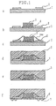
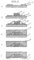
- a nickel layer of 0.001 mm in thickness (not shown in FIG. 1) was plated on one side of an electrolytic copper foil 1 of 0.035 mm in thickness.
- a photosensitive dry film resist (“PHOTEC HN340", trade name; product of Hitachi Chemical Co., Ltd.) was laminated, exposed and then developed, so that a plating resist for wiring pattern was formed.
- electrolytic copper plating was conducted in a copper sulfate bath. Applied further were a nickel plating to a thickness of 0.003 mm or greater and a gold plating of 99.9% or higher purity to a thickness of 0.0003 mm or greater.
- the plating resist was next stripped off, whereby a wiring 2 was formed (FIG. 1a).
- an LSI chip 3 was mounted (FIG. 1b).
- a silver paste 4 for semiconductors was used for bonding the LSI chip.
- LSI terminals and the wiring 2 was connected by wire bonds 100 (FIG. 1c).
- the thus-formed assembly was loaded in a die for transfer mold and sealed with a semiconductor-sealing epoxy resin ("CL-7700", trade name; product of Hitachi Chemical Co., Ltd.) 5 (FIG. 1d). Thereafter, only the copper foil 1 was dissolved away with an alkali etchant to expose the nickel. The nickel layer was removed with a nickel stripper having low copper-dissolving power so that the wiring portions were exposed (FIG. 1e).
- solder resist 6 was coated and patterned in such a way that connecting terminal portions were exposed.
- Solder balls 7 were arranged at the exposed portions of the wiring and were caused to fuse there (FIG. 1f). The wiring could be connected to an outer wiring via these solder balls 7.
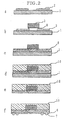
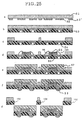
- a copper foil 1 with a wiring 2 was prepared (FIG. 2a).
- An LSI chip 3 was mounted.
- the LSI chip was provided with gold bumps 8 at terminal portions. These gold bumps 8 and terminal portions of the wiring 2 were connected together by thermocompression (FIG. 2b).
- a liquid epoxy resin 9 was filled underneath the LSI chip and cured (FIG. 2c).
- the thus-formed assembly was loaded in a die for transfer mold and sealed with a semiconductor-sealing epoxy resin ("CL-7700", trade name; product of Hitachi Chemical Co., Ltd.) 10 (FIG. 2d). Thereafter, only the copper foil 1 was dissolved away with an alkali etchant to expose the nickel.
- the nickel layer was removed with a nickel stripper having low copper-dissolving power so that the wiring portions were exposed (FIG. 2e). Then, a solder resist 6 was coated and patterned in such a way that connecting terminal portions were exposed. Solder balls 7 were arranged at the exposed portions of the wiring and were caused to fuse there (FIG. 2f). The wiring could be connected to an outer wiring via these solder balls 7.
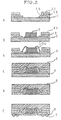
- a nickel layer of 0.001 mm in thickness (not shown in FIG. 3) was plated on one side of an electrolytic copper foil 1 of 0.035 mm in thickness.
- a photosensitive dry film resist (“PHOTEC HN340", trade name; product of Hitachi Chemical Co., Ltd.) was laminated, exposed and then developed, so that a plating resist for wiring pattern was formed.
- electrolytic copper plating was conducted in a copper sulfate bath, so that a first wiring 13 was formed.
- the plating resist was next stripped off and the first wiring 13 was subjected at a surface thereof to oxidation treatment and reduction treatment.
- the terminal portions was applied with a nickel plating to a thickness of 0.003 mm or greater and further with a gold plating of 99.9% or higher purity to a thickness of 0.0003 mm or greater (FIG. 3a).
- an LSI chip was mounted on the copper foil 1 with the two-layer wiring pattern formed thereon as described above.
- a silver paste for semiconductors was used (FIG. 3b).
- LSI terminals and the wiring 13 were connected by wire bonds 100 (FIG. 3c).
- the thus-formed assembly was loaded in a die for transfer mold and sealed with a semiconductor-sealing epoxy resin ("CL-7700", trade name; product of Hitachi Chemical Co., Ltd.) 5.
- solder resist 6 was coated and patterned in such a way that connecting terminal portions were exposed. Solder balls 7 were arranged at the exposed portions and were caused to fuse there (FIG. 3f). The wiring could be connected to an outer wiring via these solder balls 7.
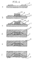
- a photosensitive dry film resist ("PHOTEC HN340", trade name; product of Hitachi Chemical Co., Ltd.) was laminated, exposed and then developed, so that a plating resist for wiring pattern was formed. Subsequently, electrolytic copper plating was conducted in a copper sulfate bath. Applied further were a nickel plating to a thickness of 0.003 mm or greater and a gold plating of 99.9% or higher purity to a thickness of 0.0003 mm or greater. The plating resist was next stripped off, whereby a wiring 2 was formed (FIG. 4a).
- a semiconductor chip 103 was mounted (FIG. 4b).
- a silver paste 4 for semiconductors was used for bonding the semiconductor chip.
- semiconductor terminals and the wiring 2 were connected by wire bonds 100 (FIG. 4c).
- the thus-formed assembly was loaded in a die for transfer mold and sealed with a semiconductor-sealing epoxy resin ("CL-7700", trade name; product of Hitachi Chemical Co., Ltd.) 5 (FIG. 4d).
- the SUS sheet 14 was mechanically stripped off to expose the wiring portion (FIG. 4e).
- a solder resist 6 was coated and patterned in such a way that connecting terminal portions were exposed.
- Solder balls 7 were arranged at the exposed portions of the wiring and were caused to fuse there (FIG. 4f).
- the wiring could be connected to an outer wiring via these solder balls 7.
- a photosensitive dry film resist ("PHOTEC HN340", trade name; product of Hitachi Chemical Co., Ltd.) was laminated, exposed and then developed, so that a plating resist for wiring pattern was formed.
- electrolytic copper plating is conducted in a copper sulfate bath.
- a nickel plating to a thickness of 0.003 mm or greater and a gold plating of 99.9% or higher purity to a thickness of 0.0003 mm or greater.
- the plating resist was next stripped off, whereby a wiring 2 was formed (FIG. 5a).
- a semiconductor chip 103 was mounted (FIG. 5b).
- a silver paste 4 for semiconductors was used for bonding the semiconductor chip.
- semiconductor terminal portions and the wiring 2 were connected by wire bonds 100 (FIG. 5c).
- the thus-formed assembly was loaded in a die for transfer mold and sealed with a semiconductor-sealing epoxy resin ("CL-7700", trade name; product of Hitachi Chemical Co., Ltd.) 5 (FIG. 5d).
- the copper foil 1 was dissolved away with an alkali etchant to expose the wiring portions of nickel (FIG. Se).
- a solder resist 6 was coated and patterned in such a way that connecting terminal portions were exposed.
- Solder balls 7 were arranged at the exposed portions of the wiring and were caused to fuse there (FIG. 5f).
- the wiring could be connected to an outer wiring via these solder balls 7.
- a photosensitive dry film resist ("PHOTEC HN340", trade name; product of Hitachi Chemical Co., Ltd.) was laminated, exposed and then developed, so that a plating resist for wiring pattern was formed. Applied further were a gold plating of 99.9% or higher purity to a thickness of 0.0003 mm or greater and a nickel plating to a thickness of 0.003 mm or greater. Further, electrolytic copper plating was conducted in a copper sulfate bath, and the plating resist was stripped off, whereby a wiring 2 is formed (FIG. 6a).
- a polyimide film 16 was bonded, connecting terminal portions of the wiring 2 were exposed by a laser (FIG. 6b), and the copper foil 1 was etched off (FIG. 6c).
- a photosensitive film in place of the polyimide film 16 made it possible to expose connecting terminal portions without using a laser.
- an LSI chip 3 was mounted on the surface of the polyimide film 16 on which the wiring pattern was formed.
- a silver paste 4 for semiconductors was used for bonding the LSI chip.
- semiconductor terminal portions and the wiring 2 were connected by wire bonds 100 (FIG. 6d).
- the thus-formed assembly was loaded in a die for transfer mold and sealed with a semiconductor-sealing epoxy resin ("CL-7700", trade name; product of Hitachi Chemical Co., Ltd.) 5 (FIG. 6e). Thereafter, solder balls 7 were arranged at the connecting terminal portions and are caused to fuse there (FIG. 6f). The wiring could be connected to an outer wiring via these solder balls 7.
- CL-7700 semiconductor-sealing epoxy resin
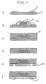
- a nickel layer of 0.001 mm in thickness (not shown in FIG. 7) was plated on one side of an electrolytic copper foil 1 of 0.035 mm in thickness.
- a photosensitive dry film resist (“PHOTEC HN340", trade name; product of Hitachi Chemical Co., Ltd.) was laminated, exposed and then developed, so that a plating resist for wiring pattern was formed.
- electrolytic copper plating was conducted in a copper sulfate bath. Applied further were a nickel plating to a thickness of 0.003 mm or greater and a gold plating of 99.9% or higher purity to a thickness of 0.0003 mm or greater.
- the plating resist was next stripped off, whereby a wiring 2 was formed (FIG. 7a).
- an LSI chip 3 was mounted on the copper foil 1 with the wiring 2 formed thereon as described above.
- a silver paste 4 for semiconductors was used for bonding the LSI chip.
- semiconductor terminal portions and the wiring 2 were connected by wire bonds 100 (FIG. 7b).
- the thus-formed assembly was loaded in a die for transfer mold and sealed with a semiconductor-sealing epoxy resin ("CL-7700", trade name; product of Hitachi Chemical Co., Ltd.) 5 (FIG. 7c). Thereafter, only the copper foil 1 was dissolved away with an alkali etchant to expose the nickel. The nickel layer was removed with a nickel stripper having low copper-dissolving power so that the wiring portion was exposed (FIG. 7d).
- solder balls 7 were arranged at the exposed portions of the wiring and are caused to fuse there (FIG. 7f). The wiring can be connected to an outer wiring via these solder balls 7.
- a photosensitive dry film resist ("PHOTEC HN340", trade name; product of Hitachi Chemical Co., Ltd.) was laminated, exposed and then developed, so that a plating resist for wiring pattern was formed. Applied further were a gold plating of 99.9% or higher purity to a thickness of 0.0003 mm or greater and a nickel plating to a thickness of 0.003 mm or greater. Further, electrolytic copper plating was conducted in a copper sulfate bath, and the plating resist was stripped off, whereby a wiring 2 was formed (FIG. 8a).
- a liquid sealing resin 17 was coated by screen printing, and an insulating layer was formed in such a manner that connecting terminal portions of the wiring 2 were exposed (FIG. 8b).
- the copper foil 1 was etched off (FIG. 8c).
- an LSI chip 3 was mounted on the surface of the hardened liquid sealing resin 16 in which the wiring pattern exist.
- a silver paste 4 for semiconductors was used for bonding the LSI chip.
- semiconductor terminal portions and the wiring 2 were connected by wire bonds 100 (FIG. 8d).
- the thus-formed assembly was loaded in a die for transfer mold and sealed with a semiconductor-sealing epoxy resin ("CL-7700", trade name; product of Hitachi Chemical Co., Ltd.) 5 (FIG. 8e). Thereafter, solder balls 7 were arranged at the connecting terminal portions of the wiring 2 and were caused to fuse there (FIG. 8f). The wiring could be connected to an outer wiring via these solder balls 7.
- CL-7700 semiconductor-sealing epoxy resin
- a nickel layer of 0.001 mm in thickness (not shown in FIG. 9) was plated on one side of an electrolytic copper foil 1 of 0.035 mm in thickness.
- a photosensitive dry film resist (“PHOTEC HN340", trade name; product of Hitachi Chemical Co., Ltd.) was laminated, exposed and then developed, so that a plating resist for wiring pattern was formed.
- electrolytic copper plating was conducted in a copper sulfate bath. Applied further were a nickel plating to a thickness of 0.003 mm or greater and a gold plating of 99.9% or higher purity to a thickness of 0.0003 mm or greater.
- the plating resist is next stripped off, whereby a wiring 2 is formed (FIG. 9a).
- an LSI chip 3 is mounted on the copper foil 1 with the wiring 2 formed thereon as described above.
- a silver paste 4 for semiconductors was used for bonding the LSI chip 3.
- semiconductor terminals and the wiring 2 were connected by wire bonds 100 (FIG. 9b).
- the thus-formed assembly was loaded in a die for transfer mold and sealed with a semiconductor-sealing epoxy resin ("CL-7700", trade name; product of Hitachi Chemical Co., Ltd.) 5 (FIG. 9c). Thereafter, only the copper foil 1 was dissolved away with an alkali etchant to expose the nickel. The nickel layer was removed with a nickel stripper having low copper-dissolving power so that the wiring portion was exposed (FIG. 9d).
- a nickel layer of 0.001 mm in thickness (not shown in FIG. 10) was plated on one side of an electrolytic copper foil 1 of 0.035 mm in thickness.
- a photosensitive dry film resist (“PHOTEC HN340", trade name; product of Hitachi Chemical Co., Ltd.) was laminated, exposed and then developed, so that a plating resist for a wiring pattern and registration marks was formed.
- electrolytic copper plating is conducted in a copper sulfate bath. Applied further are a nickel plating to a thickness of 0.003 mm or greater and a gold plating of 99.9% or higher purity to a thickness of 0.0003 mm or greater.
- the plating resist was next stripped off, whereby a wiring 2 and registration marks 18 were formed (FIG. 10a). Only portions with the registration marks 18 formed thereon were held between SUS sheets and then pressed, whereby the registration marks were caused to appear on the back side of the copper foil 1 as if they were die-stamped (FIG. 10b). On the copper foil 1 with the wiring 2 and the registration mark 18 formed thereon as described above, an LSI chip 3 was mounted (FIG. 10c). For bonding the LSI chip 3, a silver paste 4 for semiconductors was used. Next, semiconductor terminals and the wiring 2 were connected by wire bonds 100 (FIG. 10d).
- a photosensitive dry film resist ("PHOTEC HN340", trade name; product of Hitachi Chemical Co., Ltd.) was laminated, exposed and then developed, so that a plating resist for plural sets of wiring patterns was formed. Applied further were a gold plating of 99.9% or higher purity to a thickness of 0.0003 mm or greater and a nickel plating to a thickness of 0.003 mm or greater. Further, electrolytic copper plating was conducted in a copper sulfate bath, and the plating resist was stripped off, whereby plural sets of wiring 2 were formed (FIG. 11a).
- the thus-formed assembly was loaded in a die for transfer mold and sealed with a semiconductor-sealing epoxy resin ("CL-7700", trade name; product of Hitachi Chemical Co., Ltd.) 5 (FIG. 11e). Thereafter, solder balls 7 were arranged at the connecting terminal portions of the wiring 2 and were caused to fuse there (FIG. 11f). The wiring could be connected to outer wiring via these solder balls 7, respectively. Finally, the packages connected together with the polyimide film were punched out by dies (FIG. 11g).
- FIG. 12a An adhesive-coated polyimide film 20 of 0.07 mm in thickness was punched by dies to form openings at portions where connecting terminals were to be formed (FIG. 12a).
- a copper foil 21 of 0.035 mm in thickness (FIG. 12b)
- a photosensitive dry film resist (“PHOTEC HN340", trade name; product of Hitachi Chemical Co., Ltd.)waslaminated, exposed and then developed, so that an etching resist for plural sets of wiring patterns was formed.
- the copper foil wasetched and the resist was stripped off, then plural sets of wiring patterns 2 was formed (FIG. 12c). After the plural sets of wiring patterns were formed on the single polyimide film as described above, LSI chips 3 were mounted.
- die-bonding tapes 4' for semiconductors were used for bonding the LSI chips 3.
- semiconductor terminal portions and the wiring 2 were connected by wire bonds 100 (FIG. 12d).
- the thus-formed assembly was loaded in a die for transfer mold and sealed with a semiconductor-sealing epoxy resin ("CL-7700", trade name; product of Hitachi Chemical Co., Ltd.) 5 (FIG. 12e).
- solder balls 7 were arranged at the connecting terminal portions of the wiring and were caused to fuse there (FIG. 12f).
- the wiring could be connected to outer wiring via these solder balls 7.
- the packages connected together with the polyimide film were punched out by dies (FIG. 12g).
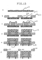
- a nickel layer of 0.001 mm in thickness (not shown in FIG. 13) was plated on one side of an electrolytic copper foil 1 of 0.035 mm in thickness.
- a photosensitive dry film resist (“PHOTEC HN340", trade name; product of Hitachi Chemical Co., Ltd.) was laminated, exposed and then developed, so that a plating resist for plural sets of wiring patterns was formed.
- electrolytic copper plating was conducted in a copper sulfate bath. Applied further were a nickel plating to a thickness of 0.003 mm or greater and a gold plating of 99.9% or higher purity to a thickness of 0.0003 mm or greater. The plating resist was stripped off, whereby wiring 2 were formed (FIG. 13a).
- the copper foil 1 with the wiring 2 formed thereon were divided into individual units and bonded to a separately-prepared stainless steel frame 22 (thickness: 0.135 mm) via a polyimide adhesive film (FIG. 13b).
- a copper alloy such as phosphor bronze, a copper foil, a nickel foil, a nickel alloy foil or the like could also be used.
- inter alia bonding making use of an intermetallic eutectic reaction or bonding making use of an ultrasonic wave.
- FIG. 14 it is desired to inspect the wiring on the copper foil 1 beforehand, to select only connection non-defectives 23 and then to bond the thus-selected connection non-defectives to the frame 22.
- FIG. 14 there were shown the electrolytic copper foil 1, the frame 22, connection defectives 24, and registration holes 25. Although each cut-off copper foil was provided with one wiring in this embodiment, plural sets of wiring may be arranged on each cut-off copper foil. As a positional relationship between the frame 22 and each copper foil upon bonding them together, various positional relationships were feasible as shown by way of example in FIGS. 15(a) and 15(b).
- FIG. 15 shows the frame 22 in plan view, in which there were illustrated an opening 26 in the frame, a mounting position 27 for the copper foil with the wiring, and a foil-fixing adhesive 28.
- LSI chips 3 were mounted, and semiconductor terminal portions and their corresponding wiring 2 were connected by wire bonds 100 (FIG. 13c).
- die-bonding tapes 4' for semiconductors were used for mounting the LSI chips.
- die-bonding silver paste or the like could be used instead of the bonding tapes 4'.
- a conventional wire-bonding method was used for the mounting of semiconductor chips.
- Other methods such as Flip chips may also be used.
- the thus-formed assembly was loaded in a die for transfer mold and sealed with a semiconductor-sealing epoxy resin ("CL-7700", trade name; product of Hitachi Chemical Co., Ltd.) 5 (FIG. 13d). Thereafter, only the copper foil 1 was dissolved away with an alkali etchant to expose the nickel. The nickel layer was removed with a nickel stripper having low copper-dissolving power so that the wiring portions were exposed.
- CL-7700 semiconductor-sealing epoxy resin
- solder resist 6 was coated and patterned in such a way that connecting terminal portions were exposed.
- Solder balls 7 were arranged at the exposed portions of the wiring and were caused to fuse there (FIG. 13e).
- the thus-obtained assembly was cut apart by a cutter and unnecessary cut pieces 101 of the frame 22 were eliminated, so that the assembly was divided into individual semiconductor packages (FIG. 13f).
- Each wiring could be connected to an outer wiring via its corresponding solder balls 7.
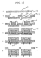
- An adhesive-coated polyimide film 29 of 0.07 mm in thickness was punched by dies to form openings at portions where connecting terminal portions were to be formed.
- a photosensitive dry film resist (“PHOTEC HN340", trade name; product of Hitachi Chemical Co., Ltd.) was laminated, exposed and then developed, so that an etching resist for plural sets of wiring patterns was formed.
- the copper foil was etched and the resist was stripped off, whereby plural sets of wiring 2 were formed (FIG. 16a).
- the connecting terminal portions and the wiring 2 were be formed using a material which was formed of a copper foil and a polyimide coated directly on the copper foil (for example, "50001", trade name; product of Hitachi Chemical Co., Ltd.).
- the formation of the openings could be effected by drilling, laser beam machining such as excimer laser machining, printing or the like.
- they could also be formed by using a material, which has been obtained by imparting photosensitivity to a polyimide, and conducting exposure and development.
- the polyimide another material such as a sealing resin could also be used.
- the wiring-formed film was divided into units. They were then bonded to a separately-prepared stainless steel frame 22 (thickness: 0.135 mm) via a polyimide adhesive 28 (FIG. 16b). Then, LSI chips 3 were mounted, and semiconductor terminal portions and the corresponding wiring 2 were connected by wire bonds 100 (FIG. 16c). For the mounting of the LSI chips, die-bonding tapes 4' for semiconductors were used. The thus-formed assembly was loaded in a die for transfer mold and sealed with a semiconductor-sealing epoxy resin ("CL-7700", trade name; product of Hitachi Chemical Co., Ltd.) 5 (FIG. 16d).
- CL-7700 semiconductor-sealing epoxy resin
- solder balls 7 were arranged in the openings, which were formed in the beginning and were to be converted to connecting terminal portions, and were caused to fuse there (FIG. 16e).
- the wiring could be connected to outer wiring via these solder balls 7, respectively.
- the packages connected together with the frame were punched out by dies into individual packages (FIG. 16f).
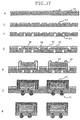
- a two-layer flexible base material was composed of a metal foil 31 and an insulating base material 32 formed directly thereon (FIG. 17a).
- a predetermined resist pattern was formed on the metal foil.
- desired plural sets of wiring patterns 33 were formed, and the resist pattern was then stripped off (FIG. 17b).
- a composite metal foil which has a thin copper layer on a carrier foil removable in a subsequent step, or the like could also be used besides a single foil such as an electrolytic copper foil, a rolled copper foil or a copper alloy foil.
- a metal foil - which was obtained by forming a nickel-phosphorus plating layer of 0.2 ⁇ m or so in thickness on one side of an electrolytic copper foil of 18 ⁇ m in thickness and then plating a thin copper layer to a thickness of 5 ⁇ m or so - was applicable.
- the thin copper layer was exposed by etching off the copper foil and nickel-phosphorus layer subsequent to formation of a polyimide layer on the thin copper layer.
- the thin copper layer may be patterned after the thin copper layer was exposed in its entirety, or the carrier foil (copper foil/thin nickel layer) may be used as a part of a leadframe structure.
- a polyimide material is ordinary from the viewpoint of process heat resistance and the like.
- the polyimide a polyimide containing 70 mole % or more of a polyimide having repeating units represented by the following formula (1) because a marked warp would be developed in the base material in a solder reflowing step if the polyimide and the copper foil had different coefficients of thermal expansion:
- holes 34 reaching the copper foil were formed at positions which were to be converted to connecting portions to an external substrate in a subsequent step (FIG. 17c).
- No particular limitation was imposed on the method for the formation of the holes.
- a laser beam machining making use of an excimer laser, CO 2 laser or YAG laser, a wet etching process and so on is applicable.
- a frame base material 37 which was coated with an adhesive 36 and has been punched out at predetermined portions (openings 35) by punching or the like, was then bonded to surfaces of the wiring patterns (FIG. 17d).
- a polyimide film or a metal foil such as a copper foil is applicable. If the thickness of the polyimide layer of the two-layer flexible base material was 25 ⁇ m and the bonded frame base material is a polyimide film, a film thickness as much as 50 to 70 ⁇ m was required to assure sufficient rigidity for the whole frame.
- no particular limitation was imposed on the area where the frame base material layer was formed.
- the frame base material layer in areas where semiconductor chips were to be mounted. Specifically, where the mounting of chips was effected by the wire-bonding method, the frame base material layer may be arranged in the entire area insofar as at least terminal portions 38 were exposed for wire-bonding. Semiconductor chips 39 were then mounted, and the semiconductor chips and the wiring patterns were electrically connected together by gold wires 40 (FIG. 17e). Where a face-down method was adopted as a mounting method for semiconductor chips, on the other hand, the wiring patterns were provided with metal bumps or the like at predetermined positions (which correspond to the positions of external connection electrodes of the semiconductor chips), and the semiconductor chips and the wiring patterns may be electrically connected together via the metal bumps.
- the thus-obtained assembly was then loaded in a die for transfer mold and was sealed with a resinous sealing material 41 (FIG. 17f).
- a resinous sealing material 41 (FIG. 17f).
- As a method for the formation of the connecting portions 42 it was possible to apply a method such that bumps were formed beforehand to a thickness greater than the polyimide film by an electrolytic plating process after the step of FIG. 17c or solder bumps were formed by a solder printing process after sealing with the resin.
- the package portions were cut off from the frame so that packages were obtained as desired (FIG. 17g).
- a two-layer flexible base material having an electrolytic copper foil of 12 ⁇ m in thickness on one side thereof (“MCF 5000I", trade name; product of Hitachi Chemical Co., Ltd.) was provided.
- a dry film resist (“PHOTEC HK815", trade name; product of Hitachi Chemical Co., Ltd.) was laminated on the copper foil and then exposed and developed, whereby a desired resist pattern was obtained. After the copper foil was etched with a solution of ferric chloride, the resist pattern was stripped with a solution of potassium hydroxide so that a predetermined wiring pattern was obtained.
- an excimer laser beam machine (“INDEX 200", trade name; manufactured by Sumitomo Heavy Industries, Ltd.), as many holes as needed (diameter: 300 ⁇ m) were formed at predetermined positions so that they extend from a side of an insulating base material and reach a back surface of the wiring pattern.
- the following conditions were set for the excimer laser beam machining - energy density: 250 mJ/cm 2 , reduction ratio: 3.0, oscillation frequency: 200 Hz, and illumination pulse number: 300 pulses.
- thermocompression bonding a 10- ⁇ m thick polyimide-base adhesive ("AS 2250", trade name; product of Hitachi Chemical Co., Ltd.) on one side of a 50- ⁇ m thick polyimide film ("UPILEX S”, trade name; product of Ube Industries, Ltd.).
- Predetermined areas including those corresponding to terminal portions to be used for wire bonding in a subsequent step were removed by punching, and the polyimide film and the two-layer flexible base material with the wiring pattern formed thereon were subjected to thermocompression via the adhesive.
- the following conditions were set for the thermo compression bonding - pressure: 20 kgf/cm 2 , temperature: 180°C, and thermocompression time: 60 minutes.
- the terminal portions for the wire bonding were next applied with nickel/gold platings.
- the thicknesses of these platings were 3 ⁇ m and 0.3 ⁇ m, respectively.
- semiconductor-chip-mounting die-bonding material (“HM-1", trade name; product of Hitachi Chemical Co., Ltd.)
- HM-1 semiconductor-chip-mounting die-bonding material
- the mounting conditions were set as follows - press pressure: 5 kgf/cm 2 , bonding temperature: 380°C, and compression-bonding time: 5 seconds. External electrode portions of each semiconductor chip were then electrically connected with its corresponding wiring pattern by wire bonding.
- the thus-obtained assembly was stamped into a leadframe-shaped form, loaded in a die for transfer mold and then sealed at 185°C for 90 seconds with a semiconductor-sealing epoxy resin ("CL-7700", trade name; product of Hitachi Chemical Co., Ltd.).
- CL-7700 semiconductor-sealing epoxy resin
- the above-mentioned holes were then each coated with a predetermined amount of solder by a printing process.
- the solder was caused to fuse in an infrared reflowing oven, so that external connection bumps were formed.
- the package portions were punched out by dies so that packages were obtained as desired.
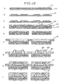
- a two-layer flexible base material was composed of a metal foil 31 and an insulating base material 32 formed directly thereon (FIG. 18a).
- a predetermined resist pattern was formed on the metal foil.
- desired plural sets of wiring patterns 33 were formed, and the resist pattern was then stripped off (FIG. 18b).
- a composite metal foil which had a thin copper layer on a carrier foil removable in a subsequent step, or the like could also be used besides a single foil such as an electrolytic copper foil, a rolled copper foil or a copper alloy foil.
- a metal foil - which was obtained by forming a nickel-phosphorus plating layer of 0.2 ⁇ m or so in thickness on one side of an electrolytic copper foil of 18 ⁇ m in thickness and then plating a thin copper layer to a thickness of 5 ⁇ m or so - was applicable.
- the thin copper layer was exposed by etching off the copper foil and nickel-phosphorus layer subsequent to formation of a polyimide layer on the thin copper layer.
- the thin copper layer might be patterned after the thin copper layer was exposed in its entirety, or the carrier foil (copper foil/thin nickel layer) might be used as a part of a leadframe structure.
- a polyimide material was ordinary from the viewpoint of process heat resistance and the like.
- the polyimide a polyimide containing 70 mole % or more of a polyimide having repeating units represented by the formula (1) because a marked warp would be developed in the base material in a solder reflowing step if the polyimide and the copper foil had different coefficients of thermal expansion.
- holes 34 reaching the copper foil were formed at positions which were to be converted to connecting portions to external substrate in a subsequent step (FIG. 18c).
- No particular limitation was imposed on the method for the formation of the holes.
- a wet etching process or the like was applicable.
- a frame base material 37 which was coated with an adhesive 36 and had been punched out at predetermined portions (openings 35) by punching or the like, is then bonded as a second insulating base material to surfaces of the wiring patterns (FIG. 18d).
- the thickness of the polyimide layer of the two-layer flexible base material is 25 ⁇ m, a film thickness as much as 50 to 70 ⁇ m was required as a thickness of a polyimide film to be bonded in view of a subsequent step in which the polyimide film is fixed on a frame.
- no particular limitation was imposed on the area where the polyimide was bonded. Its arrangement in areas where semiconductor chips were to be mounted made it possible to form external connection terminals under the semiconductor chips like CSPs.
- the polyimide film might be bonded in the entire area insofar as at least terminal portions 38 were exposed for wire-bonding.
- the insulating substrate obtained as described above was divided into the individual wiring patterns (FIG. 18e) and were then fixed on a separately-prepared frame 43 made, for example, of SUS or the like (FIG. 18f).
- Semiconductor chips 39 were then mounted, and the semiconductor chips and the wiring patterns were electrically connected together by gold wires 40 (FIG. 18g).
- the wiring patterns were provided with metal bumps or the like at predetermined positions (which correspond to the positions of external connection electrodes of the semiconductor chips), and the semiconductor chips and the wiring patterns might be electrically connected together via the metal bumps.
- the thus-obtained assembly was then loaded in a die for transfer mold and was sealed with a resinous sealing material 41 (FIG. 18h).
- a resinous sealing material 41 (FIG. 18h).
- an epoxy resin containing 5 to 80 wt.% of silica of about 10 to 20 ⁇ m in diameter could be used.
- the connecting portions 42 As a method for the formation of the connecting portions 42 it was possible to apply a method such that bumps were formed beforehand to a thickness greater than the polyimide film by an electrolytic plating process after the step of FIG. 18c or solder bumps were formed by a solder printing process after sealing with the resin. Finally, the package portions were cut off from the frame so that packages were obtained as desired (FIG. 18i).
- FIG. 18 The sixteenth embodiment of FIG. 18 will be described more specifically.
- a two-layer flexible base material having an electrolytic copper foil of 12 ⁇ m in thickness on one side thereof (“MCF 5000I", trade name; product of Hitachi Chemical Co., Ltd.) was provided.
- a dry film resist (“PHOTEC HK815", trade name; product of Hitachi Chemical Co., Ltd.) was laminated on the copper foil and then exposed and developed, whereby a desired resist pattern was obtained. After the copper foil was etched with a solution of ferric chloride, the resist pattern was stripped with a solution of potassium hydroxide so that a predetermined wiring pattern was obtained.
- an excimer laser beam machine (“INDEX 200", trade name; manufactured by Sumitomo Heavy Industries, Ltd.), as many holes as needed (diameter: 300 ⁇ m) were formed as many as needed at predetermined positions so that they extend from a side of an insulating base material and reach a back surface of the wiring pattern.
- the following conditions were set for the excimer laser beam machining - energy density: 250 mJ/cm 2 , reduction ratio: 3.0, oscillation frequency: 200 Hz, and illumination pulse number: 300 pulses.
- thermocompression bonding a 10- ⁇ m thick polyimide-base adhesive ("AS 2250", trade name; product of Hitachi Chemical Co., Ltd.) on one side of a 50- ⁇ m thick polyimide film ("UPILEX S”, trade name; product of Ube Industries, Ltd.).
- Predetermined areas including those corresponding to terminal portions to be used for wire bonding in a subsequent step were removed by punching, and the polyimide film and the two-layer flexible base material with the wiring pattern formed thereon were subjected to thermocompression via the adhesive.
- the following conditions were set for the thermo compression bonding - pressure: 20 kgf/cm 2 , temperature: 180°C, and thermocompression time: 60 minutes.
- the terminal portions for the wire bonding were next applied with nickel/gold platings.
- the thicknesses of these platings were 3 ⁇ m and 0.3 ⁇ m, respectively.
- the thus-obtained substrate was divided into the individual wiring patterns and are fixed on a separately-prepared SUS frame.
- semiconductor-chip-mounting die-bonding material ("HM-1", trade name; product of Hitachi Chemical Co., Ltd.)
- semiconductor chips were then mounted.
- the mounting conditions were set as follows - press pressure: 5 kgf/cm 2 , bonding temperature: 380°C, and compression-bonding time: 5 seconds.
- External electrode portions of each semiconductor chip were then electrically connected with its corresponding wiring pattern by wire bonding.
- the thus-obtained assembly was molded into a lead frame-shaped form, loaded in a die for transfer mold and then sealed at 185°C for 90 seconds with a semiconductor-sealing epoxy resin ("CL-7700", trade name; product of Hitachi Chemical Co., Ltd.).
- CL-7700 semiconductor-sealing epoxy resin
- the above-mentioned holes were then each coated with a predetermined amount of solder by a printing process.
- the solder was caused to fuse in an infrared reflowing oven, so that external connection bumps were formed.
- the package portions were punched out by dies so that packages were obtained as desired.
- Plural sets of predetermined wiring patterns 52 were formed on a supporting member 51 (FIG. 19a).
- an insulating base material such as a polyimide film could be used besides a metal foil such as an electrolytic copper foil.
- an insulating base material there were two methods. According to the first method, nonthrough-holes reaching the wiring patterns were formed at predetermined positions of the insulating base material, and external connection terminals were formed at exposed portions of the wiring patterns. The nonthrough-holes could be formed by applying an excimer laser or a CO 2 laser and so on. According to the second method, a drilled insulating base material provided with an adhesive was formed in advance and, subsequent to lamination with an electrolytic copper foil or the like, the copper foil was subjected to etching.
- a resist pattern was formed with a photoresist and wiring patterns were then formed by electroplating while using the metal foil as a cathode.
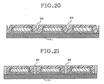
- FIG. 20 shows grooves 59 formed in boundary portions between individual package portions. The width, depth and the like of each groove could be modified depending on the dimensions which the die for transfer mold could receive for processing.
- FIG. 21 illustrates a transfer molding process which was carried out using a grid-shaped intermediate plate 60 hollowed out beforehand at areas corresponding to the individual package portions.
- the supporting member was a metal foil
- the supporting member was removed by a chemical etching process and external connection terminals 57 were formed at predetermined positions (FIG. 19d).
- an insulating base material was used as a supporting member, it was only necessary to selectively remove the insulating base material at predetermined areas by a laser or the like.
- the substrate which had been sealed as a whole is cut apart into unit portions 58.
- a solder resist layer might be formed on exposed surfaces of the wiring patterns for protecting the wiring patterns.
- the resultant assembly was dried at 85°C for 15 minutes and then cut into the individual blocks.
- semiconductor-device-mounting die-bonding material ("HM-1", trade name; product of Hitachi Chemical Co., Ltd.)
- HM-1 semiconductor-device-mounting die-bonding material
- the bonding conditions were set as follows - press pressure: 5 kgf/cm 2 , temperature: 380°C, and compression-bonding time: 5 seconds.
- External terminals of each semiconductor device were then electrically connected with its corresponding gold-plated terminal portions (second connecting portions) by wire bonding.
- the thus-obtained assembly was loaded in a die for transfer mold.
- the 75 wiring patterns (corresponding to 1 block) were sealed all together at 185°C for 90 seconds so that the individual wiring patterns were transferred into the sealing material.
- the electrolytic copper foil was etched off at desired portions with an alkali etchant ("A Process", trade name; product of Japan Meltex, Inc.).
- the temperature and spraying pressure of the etching solution were 40°C and 1.2 kgf/cm 2 , respectively.
- Solder patterns were then formed at external connection terminal portions by a printing process. The solder was caused to fuse in an infrared reflowing oven, so that external connection bumps were formed. Finally, the assembly was divided into individual package portions by a diamond cutter so that packages were obtained as desired.
- the resultant assembly was dried at 85°C for 15 minutes and then cut into the individual blocks.
- a semiconductor-device-mounting die-bonding material ("HM-1", trade name; product of Hitachi Chemical Co., Ltd.)
- the semiconductor devices were then bonded.
- the bonding conditions were set as follows - press pressure: 5 kgf/cm 2 , temperature: 380°C, and compression-bonding time: 5 seconds.
- External terminals of each semiconductor device were then electrically connected with its corresponding gold-plated terminal portions (second connecting portions) by wire bonding.
- Using as an intermediate plate a grid-shaped stainless steel plate hollowed out at areas corresponding to individual package areas, the thus-obtained assembly was loaded in a die for transfer mold.
- the 75 wiring patterns (corresponding to 1 block) were sealed all together at 185°C for 90 seconds so that the individual wiring patterns were transferred into the sealing material.
- a grid portion of the intermediate plate was tapered at 12° to facilitate separation of the individual packages from the intermediate plate.
- the electrolytic copper foil was etched off at desired portions with an alkali etchant ("A Process", trade name; product of Japan Meltex, Inc.). Each package portion was held in place by the grid-shaped intermediate plate.
- the temperature and spraying pressure of the etching solution were 40°C and 1.2 kgf/cm 2 , respectively.
- solder patterns were formed at external connection terminal portions by a printing process. The solder was caused to fuse in an infrared reflowing oven, so that external connection bumps were formed. Individual package portions were separated from the intermediate plate so that packages were obtained as desired.
- Plural sets of predetermined resist patterns 62 (FIG. 22b) were formed on an electrically-conductive temporary supporting member 61 (FIG. 22a).
- wiring patterns 63 are formed at exposed portions of the temporary supporting member by an electroplating process.
- the temporary supporting member it was possible to use a conventional electrolytic copper foil and a foil consisting of an electrolytic copper foil and a thin layer of a metal (nickel, gold, solder or the like) different in chemical etching conditions from the copper foil provided thereon. Further, copper was preferred for the wiring patterns.
- the present invention was not limited to cases making use of a face-up method as a mounting method for semiconductor devices but was also applicable to cases making use of a face-down method for example. Specifically, it was only necessary to form bumps for face-down bonding at predetermined positions on the wiring patterns 63 by a plating process or the like and then to electrically connect external connecting portions of the semiconductor devices with the bumps.
- predetermined metal patterns 69 are formed at positions corresponding to the external connection terminals (FIG. 22f).
- any metal could be used insofar as it was not etched under conditions for etching off the electrically-conductive temporary supporting member.
- solder, gold, nickel/gold or the like could be used.
- a known electroplating process or solder printing process could be applied.
- solder bumps 70 could be formed by reflowing. In this case, by adjusting the thickness of the patterns 69, it was possible to control the height of the reflowed solder bumps 70.
- the temporary supporting member was next removed at predetermined portions while using the metal patterns as an etching resist, whereby the wiring patterns were exposed.
- the assembly was divided into individual packages 71 by stamping or dicing (FIG. 22g).
- the exposed wiring patterns were not protected by a corrosion-resistant metal such as nickel, areas other than the external connection terminal portions might be coated with a known solder resist or the like.
- solder as metal patterns, no particular limitation is imposed on the reflowing step.
- the reflowing step could be performed either before or after dividing the assembly into the individual packages.
- the reflowing step could also be conducted before mounting the individual packages on external wiring boards.
- the eighteenth embodiment will be described specifically.
- Wiring patterns which were each consisted of 0.2 ⁇ m thick nickel, 30 ⁇ m thick copper, 5 ⁇ m thick nickel and 1 ⁇ m thick soft gold were next formed by an electroplating method. The resist pattern was next stripped off using a 3 wt.% solution of potassium hydroxide of 35°C.
- the electroplated copper foil was etched off at desired portions with an alkali etchant ("A Process", trade name; product of Japan Meltex, Inc.).
- the temperature and spraying pressure of the etching solution were 40°C and 1.2 kgf/cm 2 , respectively.
- the solder was caused to fuse in an infrared reflowing oven, so that external connection bumps were formed.
- FIG. 23 The construction of a semiconductor mounting frame will be described with reference to FIG. 23.
- Numeral 89 indicated semiconductor-mounting substrates, each of which consisted of an insulating base material and wiring. Plural substrates were connected together via connecting portions 90.
- Each connecting portion 90 was provided with pinholes 91 as reference positions. Recognition marks employed in image recognition might be used in place of the pinholes 91. Based on these reference positions, positioning was performed in subsequent steps. Especially upon molding semiconductors with resin, positional registration was effected by inserting pins, which were arranged inside a cavity, in the pinholes 91.
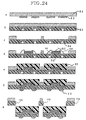
- a nickel layer of 0.001 mm in thickness (not shown in FIGS. 24 and 25) was formed by an electrolytic plating process on one side of an electrolytic copper foil 81 of about 0.070 mm in thickness which was an electrically-conductive temporary substrate.
- a photosensitive dry film resist (“PHOTEC-HN340", trade name; product of Hitachi Chemical Co., Ltd.) was laminated, followed by exposure and development so that a plating resist for plural sets of wiring patterns was formed.
- the intensity of the exposure at this time is 70 mJ/cm 2 .
- FIG. 24a electrolytic copper plating was conducted in a known copper sulfate bath and the resist is stripped off, whereby plural sets of wiring 82 were formed (FIG. 24a, FIG. 25a).
- FIG. 25a it might be contemplated to form plated copper 82' at the connecting portions too. This makes it possible to provide the resulting frame with still enhanced rigidity.
- FIG. 24a and FIG. 25a could also be obtained by providing beforehand a base material composed of three layers of copper/thin nickel layer/copper and forming one of the copper foils into wiring in a usual etching step.
- the construction of the copper foil 81/thin nickel layer (not shown)/copper wirings 82 (and 82') obtained here might be replaced by a two-layer structure free of the thin nickel layer, such as copper foil/nickel wirings, nickel foil/copper wirings, or the like.
- the selectable kinds of metals were not limited to those of the present embodiment, it was a preferred standard for the selection to allow wirings to selectively remain when some parts of the temporary substrate were etched off in a subsequent step (FIG. 24c, FIG. 25c).
- the electrically-conductive temporary substrate became a material which made up the connecting portions of the frame, a greater thickness was preferred. There was however a subsequent step to etch it off partly, so that it was necessary to select an appropriate thickness.
- the thickness of the electrically-conductive temporary substrate varies depending on the material. For example, when a copper foil was used, about 0.03 to 0.3 mm or so was preferred.
- a polyimide adhesive 83 was next applied to the wiring-containing surface of the copper foil 81 with the plural sets of wiring 82 formed thereon.
- the polyimide adhesive 83 was not limited to this material. It was possible to use, for example, an epoxy adhesive film, a film formed of a polyimide film and an adhesive coated thereon, or the like.
- holes 84 for the external connection terminals were formed using an excimer laser (FIG. 24b, FIG. 25b). For the sake of simplification of subsequent steps, it was suited to arrange connecting terminals before mounting semiconductors.
- these holes 84 As another method for the formation of these holes 84, it was possible to form beforehand the holes 84 for the external connection terminals in a film by drilling or punching and then to bond the film so formed. Although no problem or inconvenience would arise even if a metal to be employed as the connecting terminals (which was designated at numeral 88 in FIG. 24f and FIG. 25f), such as a solder or the like, was filled at this stage, the resulting metal bumps may become an obstacle in the subsequent semiconductor mounting step and resin sealing step. Thus, it was preferred to form a metal at a subsequent step. It is preferred to locate the holes for the external connection terminals (or terminals) in the mounting substrate portions for the semiconductor devices, in the form of arrays on the side opposite to the side on which the semiconductor devices were mounted.
- etching solution As this etching solution, it was preferred to choose an etching solution and etching conditions, which in the case of this embodiment, provide a substantially higher dissolution velocity for copper than for nickel.
- an alkali etchant ("A Process", trade name; product of Japan Meltex Inc.) as an etching solution and, for example, a solution temperature of 40°C and a spray pressure of 1.2 kgf/cm 2 . It was to be noted that the kind of solution and the conditions specified here are merely illustrative.
- etching solution and etching conditions so that a substantially higher dissolution velocity was provided for nickel than for copper.
- selective etching was conducted with a nickel etchant ("Melstrip N950", trade name; product of Japan Meltex, Inc.).
- the temperature and spraying pressure of the etching solution were set at 40°C and 1.2 kgf/cm 2 , respectively. It was to be noted that the kind of the solution and conditions specified here were merely illustrative.
- the temporary substrate was allowed to remain as the connecting portions, whereby a semiconductor mounting frame having rigidity was obtained (FIG. 24c, FIG. 25c).
- electroless nickel-gold plating was applied to terminal portions of the copper wirings on this frame (not shown). This is needed for wire-bonding chips in a subsequent step. Such surface treatment could be applied as needed.
- semiconductor chips 85 were then mounted.
- semiconductor die-bonding tapes 86 for example, "HM-1", trade name; product of Hitachi Chemical Co., Ltd.
- the chips might be bonded using a die-bonding silver paste.
- terminal portions of the semiconductors and the wiring were connected by wire bonds 100 (FIG. 24d, FIG. 25d).
- the connection with the terminals of the semiconductors could be effected by another method, for example, by face-down connection making use of Flip chips or by bonding making use of an anisotropic conductive adhesive.
- the assembly so formed was loaded in a die for transfer mold and was sealed using a semiconductor-sealing epoxy resin ("CL-7700", trade name; product of Hitachi Chemical Co., Ltd.) 87 (FIG. 24e, FIG. 25e). Thereafter, solder balls 88 were arranged in the connecting holes formed at connecting terminal portions of the wiring 82 and were then caused to fuse (FIG. 24f, FIG. 25f). These solder balls 88 became so-called external connection terminals. The plural semiconductor devices connected together by the connecting portions 102 were punched by dies, so that the individual semiconductor devices were obtained (FIG. 24g, FIG. 25g).
- CL-7700 semiconductor-sealing epoxy resin
- the semiconductor mounting frame and semiconductor device fabrication process made it possible to obtain a frame having sufficient rigidity in the fabrication of semiconductor devices, such as BGAs, CSPs or the like, by using a film-shaped substrate such as a polyimide tape and so on.
- semiconductor devices such as BGAs, CSPs or the like
- a film-shaped substrate such as a polyimide tape and so on.
- semiconductor packages capable of meeting the move toward higher integration of semiconductor chips could be fabricated stably with good productivity.
- a process for the fabrication of a semiconductor package which comprises the following steps:
- a process for the fabrication of a semiconductor package which comprises the following steps:
- a process for the fabrication of a semiconductor package which comprises the following steps:
- a process for the fabrication of a semiconductor package which comprises the following steps:
- a process for the fabrication of semiconductor packages which comprises the following steps:
- a process for the fabrication of semiconductor packages which comprises the following steps:
- a process for the fabrication of semiconductor packages which comprises the following steps:
- a process for the fabrication of semiconductor packages provided with a single layer of wiring, one side of said wiring having a first connecting function of being connected with a semiconductor device and an opposite side of said wiring having a second connecting function of being connected to external wiring which comprises the following steps 9A, 9B, 9C, 9D and 9E:
- a process for the fabrication of semiconductor packages which comprises the following steps:
- a semiconductor package fabricated by the process according to any one of claims 1 to 11.
- a process for the fabrication of a semiconductor device packaging frame said frame being provided with plural semiconductor-device-mounting portions, portions connecting together said plural semiconductor-device-mounting portions, and a registration mark portion, which comprises the following steps:
Landscapes
- Engineering & Computer Science (AREA)
- Manufacturing & Machinery (AREA)
- Microelectronics & Electronic Packaging (AREA)
- Structures Or Materials For Encapsulating Or Coating Semiconductor Devices Or Solid State Devices (AREA)
- Encapsulation Of And Coatings For Semiconductor Or Solid State Devices (AREA)
- Wire Bonding (AREA)
- Lead Frames For Integrated Circuits (AREA)
Applications Claiming Priority (9)
| Application Number | Priority Date | Filing Date | Title |
|---|---|---|---|
| JP4876094 | 1994-03-18 | ||
| JP4876094 | 1994-03-18 | ||
| JP27346994 | 1994-11-08 | ||
| JP27346994 | 1994-11-08 | ||
| JP768395 | 1995-01-20 | ||
| JP768395 | 1995-01-20 | ||
| JP5620295 | 1995-03-15 | ||
| JP5620295 | 1995-03-15 | ||
| EP95912471A EP0751561A4 (de) | 1994-03-18 | 1995-03-17 | Herstellungsverfahren einer halbleiterpackung und halbleiterpackung |
Related Parent Applications (1)
| Application Number | Title | Priority Date | Filing Date |
|---|---|---|---|
| EP95912471A Division EP0751561A4 (de) | 1994-03-18 | 1995-03-17 | Herstellungsverfahren einer halbleiterpackung und halbleiterpackung |
Publications (2)
| Publication Number | Publication Date |
|---|---|
| EP1213756A2 true EP1213756A2 (de) | 2002-06-12 |
| EP1213756A3 EP1213756A3 (de) | 2005-05-25 |
Family
ID=27454766
Family Applications (4)
| Application Number | Title | Priority Date | Filing Date |
|---|---|---|---|
| EP02003791A Withdrawn EP1213754A3 (de) | 1994-03-18 | 1995-03-17 | Halbleitergehäuseherstellung und Halbleitergehäuse |
| EP02003792A Withdrawn EP1213755A3 (de) | 1994-03-18 | 1995-03-17 | Halbleitergehäuseherstellung und Halbleitergehäuse |
| EP95912471A Withdrawn EP0751561A4 (de) | 1994-03-18 | 1995-03-17 | Herstellungsverfahren einer halbleiterpackung und halbleiterpackung |
| EP02003794A Withdrawn EP1213756A3 (de) | 1994-03-18 | 1995-03-17 | Halbleitergehäuseherstellung und Halbleitergehäuse |
Family Applications Before (3)
| Application Number | Title | Priority Date | Filing Date |
|---|---|---|---|
| EP02003791A Withdrawn EP1213754A3 (de) | 1994-03-18 | 1995-03-17 | Halbleitergehäuseherstellung und Halbleitergehäuse |
| EP02003792A Withdrawn EP1213755A3 (de) | 1994-03-18 | 1995-03-17 | Halbleitergehäuseherstellung und Halbleitergehäuse |
| EP95912471A Withdrawn EP0751561A4 (de) | 1994-03-18 | 1995-03-17 | Herstellungsverfahren einer halbleiterpackung und halbleiterpackung |
Country Status (6)
| Country | Link |
|---|---|
| US (5) | US5976912A (de) |
| EP (4) | EP1213754A3 (de) |
| JP (3) | JP3247384B2 (de) |
| KR (2) | KR100437436B1 (de) |
| CN (2) | CN1117395C (de) |
| WO (1) | WO1995026047A1 (de) |
Cited By (1)
| Publication number | Priority date | Publication date | Assignee | Title |
|---|---|---|---|---|
| DE102005007486A1 (de) * | 2005-02-17 | 2006-08-31 | Infineon Technologies Ag | Halbleiterbauteil mit oberflächenmontierbarem Gehäuse und Verfahren zur Herstellung desselben |
Families Citing this family (468)
| Publication number | Priority date | Publication date | Assignee | Title |
|---|---|---|---|---|
| JP4029910B2 (ja) * | 1994-03-18 | 2008-01-09 | 日立化成工業株式会社 | 半導体パッケ−ジの製造法及び半導体パッケ−ジ |
| EP1213754A3 (de) * | 1994-03-18 | 2005-05-25 | Hitachi Chemical Co., Ltd. | Halbleitergehäuseherstellung und Halbleitergehäuse |
| US6465743B1 (en) | 1994-12-05 | 2002-10-15 | Motorola, Inc. | Multi-strand substrate for ball-grid array assemblies and method |
| US5677566A (en) * | 1995-05-08 | 1997-10-14 | Micron Technology, Inc. | Semiconductor chip package |
| US6159770A (en) * | 1995-11-08 | 2000-12-12 | Fujitsu Limited | Method and apparatus for fabricating semiconductor device |
| US6376921B1 (en) | 1995-11-08 | 2002-04-23 | Fujitsu Limited | Semiconductor device, method for fabricating the semiconductor device, lead frame and method for producing the lead frame |
| US6329711B1 (en) * | 1995-11-08 | 2001-12-11 | Fujitsu Limited | Semiconductor device and mounting structure |
| US6072239A (en) * | 1995-11-08 | 2000-06-06 | Fujitsu Limited | Device having resin package with projections |
| JP3445895B2 (ja) * | 1996-02-28 | 2003-09-08 | 日立化成工業株式会社 | 半導体パッケ−ジ用チップ支持基板 |
| US6821821B2 (en) * | 1996-04-18 | 2004-11-23 | Tessera, Inc. | Methods for manufacturing resistors using a sacrificial layer |
| US6001671A (en) * | 1996-04-18 | 1999-12-14 | Tessera, Inc. | Methods for manufacturing a semiconductor package having a sacrificial layer |
| DE69735588T2 (de) * | 1996-05-27 | 2007-01-11 | Dai Nippon Printing Co., Ltd. | Herstellung eines bauteils für eine halbleiterschaltung |
| US5776798A (en) * | 1996-09-04 | 1998-07-07 | Motorola, Inc. | Semiconductor package and method thereof |
| DE19640304C2 (de) * | 1996-09-30 | 2000-10-12 | Siemens Ag | Chipmodul insbesondere zur Implantation in einen Chipkartenkörper |
| US6274405B1 (en) | 1996-10-17 | 2001-08-14 | Seiko Epson Corporation | Semiconductor device, method of making the same, circuit board, and film carrier tape |
| US6962829B2 (en) | 1996-10-31 | 2005-11-08 | Amkor Technology, Inc. | Method of making near chip size integrated circuit package |
| US5990545A (en) * | 1996-12-02 | 1999-11-23 | 3M Innovative Properties Company | Chip scale ball grid array for integrated circuit package |
| US5866949A (en) * | 1996-12-02 | 1999-02-02 | Minnesota Mining And Manufacturing Company | Chip scale ball grid array for integrated circuit packaging |
| US6635514B1 (en) * | 1996-12-12 | 2003-10-21 | Tessera, Inc. | Compliant package with conductive elastomeric posts |
| US5907769A (en) * | 1996-12-30 | 1999-05-25 | Micron Technology, Inc. | Leads under chip in conventional IC package |
| JP2982729B2 (ja) * | 1997-01-16 | 1999-11-29 | 日本電気株式会社 | 半導体装置 |
| SG63803A1 (en) | 1997-01-23 | 1999-03-30 | Toray Industries | Epoxy-resin composition to seal semiconductors and resin-sealed semiconductor device |
| US6583444B2 (en) * | 1997-02-18 | 2003-06-24 | Tessera, Inc. | Semiconductor packages having light-sensitive chips |
| KR100237328B1 (ko) * | 1997-02-26 | 2000-01-15 | 김규현 | 반도체 패키지의 구조 및 제조방법 |
| JPH10284525A (ja) * | 1997-04-03 | 1998-10-23 | Shinko Electric Ind Co Ltd | 半導体装置の製造方法 |
| JP2943788B2 (ja) | 1997-04-10 | 1999-08-30 | 日立エーアイシー株式会社 | 電子部品搭載用配線基板 |
| EP2015359B1 (de) * | 1997-05-09 | 2015-12-23 | Citizen Holdings Co., Ltd. | Herstellung von Halbleitergehäusen und Leiterplattenanordnung |
| JP3363065B2 (ja) | 1997-05-16 | 2003-01-07 | 日立化成工業株式会社 | 半導体パッケージ用チップ支持基板の製造法及び半導体装置 |
| FR2764111A1 (fr) * | 1997-06-03 | 1998-12-04 | Sgs Thomson Microelectronics | Procede de fabrication de boitiers semi-conducteurs comprenant un circuit integre |
| JP3639088B2 (ja) * | 1997-06-06 | 2005-04-13 | 株式会社ルネサステクノロジ | 半導体装置及び配線テープ |
| US6173490B1 (en) * | 1997-08-20 | 2001-01-16 | National Semiconductor Corporation | Method for forming a panel of packaged integrated circuits |
| JP2954110B2 (ja) * | 1997-09-26 | 1999-09-27 | 九州日本電気株式会社 | Csp型半導体装置及びその製造方法 |
| US5888850A (en) * | 1997-09-29 | 1999-03-30 | International Business Machines Corporation | Method for providing a protective coating and electronic package utilizing same |
| US6028354A (en) | 1997-10-14 | 2000-02-22 | Amkor Technology, Inc. | Microelectronic device package having a heat sink structure for increasing the thermal conductivity of the package |
| DE69832944T2 (de) * | 1997-10-29 | 2006-10-26 | Hitachi Chemical Co., Ltd. | Siloxanmodifizierte Polyamidharzzusammensetzung, Klebefilme, Klebefolie und Halbleiterbauelement |
| JPH11163022A (ja) * | 1997-11-28 | 1999-06-18 | Sony Corp | 半導体装置、その製造方法及び電子機器 |
| JP3819574B2 (ja) | 1997-12-25 | 2006-09-13 | 三洋電機株式会社 | 半導体装置の製造方法 |
| JPH11186432A (ja) * | 1997-12-25 | 1999-07-09 | Canon Inc | 半導体パッケージ及びその製造方法 |
| JPH11233684A (ja) * | 1998-02-17 | 1999-08-27 | Seiko Epson Corp | 半導体装置用基板、半導体装置及びその製造方法並びに電子機器 |
| TW434760B (en) * | 1998-02-20 | 2001-05-16 | United Microelectronics Corp | Interlaced grid type package structure and its manufacturing method |
| JP3481117B2 (ja) * | 1998-02-25 | 2003-12-22 | 富士通株式会社 | 半導体装置及びその製造方法 |
| US6326239B1 (en) * | 1998-04-07 | 2001-12-04 | Denso Corporation | Mounting structure of electronic parts and mounting method of electronic parts |
| JP3438586B2 (ja) | 1998-04-23 | 2003-08-18 | 松下電工株式会社 | プリント配線板の製造方法 |
| US6933594B2 (en) * | 1998-06-10 | 2005-08-23 | Asat Ltd. | Leadless plastic chip carrier with etch back pad singulation |
| US7049177B1 (en) | 2004-01-28 | 2006-05-23 | Asat Ltd. | Leadless plastic chip carrier with standoff contacts and die attach pad |
| US6989294B1 (en) | 1998-06-10 | 2006-01-24 | Asat, Ltd. | Leadless plastic chip carrier with etch back pad singulation |
| US7270867B1 (en) | 1998-06-10 | 2007-09-18 | Asat Ltd. | Leadless plastic chip carrier |
| US7226811B1 (en) | 1998-06-10 | 2007-06-05 | Asat Ltd. | Process for fabricating a leadless plastic chip carrier |
| US6872661B1 (en) | 1998-06-10 | 2005-03-29 | Asat Ltd. | Leadless plastic chip carrier with etch back pad singulation and die attach pad array |
| US6294100B1 (en) | 1998-06-10 | 2001-09-25 | Asat Ltd | Exposed die leadless plastic chip carrier |
| US8330270B1 (en) | 1998-06-10 | 2012-12-11 | Utac Hong Kong Limited | Integrated circuit package having a plurality of spaced apart pad portions |
| US7271032B1 (en) | 1998-06-10 | 2007-09-18 | Asat Ltd. | Leadless plastic chip carrier with etch back pad singulation |
| US6229200B1 (en) | 1998-06-10 | 2001-05-08 | Asat Limited | Saw-singulated leadless plastic chip carrier |
| US6635957B2 (en) | 1998-06-10 | 2003-10-21 | Asat Ltd. | Leadless plastic chip carrier with etch back pad singulation and die attach pad array |
| US6585905B1 (en) * | 1998-06-10 | 2003-07-01 | Asat Ltd. | Leadless plastic chip carrier with partial etch die attach pad |
| US7247526B1 (en) | 1998-06-10 | 2007-07-24 | Asat Ltd. | Process for fabricating an integrated circuit package |
| US6498099B1 (en) * | 1998-06-10 | 2002-12-24 | Asat Ltd. | Leadless plastic chip carrier with etch back pad singulation |
| JP2000156435A (ja) * | 1998-06-22 | 2000-06-06 | Fujitsu Ltd | 半導体装置及びその製造方法 |
| US7112474B1 (en) | 1998-06-24 | 2006-09-26 | Amkor Technology, Inc. | Method of making an integrated circuit package |
| US7005326B1 (en) | 1998-06-24 | 2006-02-28 | Amkor Technology, Inc. | Method of making an integrated circuit package |
| US7332375B1 (en) | 1998-06-24 | 2008-02-19 | Amkor Technology, Inc. | Method of making an integrated circuit package |
| US6893900B1 (en) | 1998-06-24 | 2005-05-17 | Amkor Technology, Inc. | Method of making an integrated circuit package |
| US7071541B1 (en) | 1998-06-24 | 2006-07-04 | Amkor Technology, Inc. | Plastic integrated circuit package and method and leadframe for making the package |
| US6143981A (en) | 1998-06-24 | 2000-11-07 | Amkor Technology, Inc. | Plastic integrated circuit package and method and leadframe for making the package |
| US7030474B1 (en) | 1998-06-24 | 2006-04-18 | Amkor Technology, Inc. | Plastic integrated circuit package and method and leadframe for making the package |
| DE19830159A1 (de) * | 1998-07-06 | 2000-01-20 | Siemens Ag | Chipmodul mit einem Substrat als Träger für eine ein- oder mehrlagige hochdichte Verdrahtung (High Density Interconnect) |
| US6092281A (en) | 1998-08-28 | 2000-07-25 | Amkor Technology, Inc. | Electromagnetic interference shield driver and method |
| JP4073098B2 (ja) * | 1998-11-18 | 2008-04-09 | 三洋電機株式会社 | 半導体装置の製造方法 |
| US6448633B1 (en) | 1998-11-20 | 2002-09-10 | Amkor Technology, Inc. | Semiconductor package and method of making using leadframe having lead locks to secure leads to encapsulant |
| JP3169919B2 (ja) * | 1998-12-21 | 2001-05-28 | 九州日本電気株式会社 | ボールグリッドアレイ型半導体装置及びその製造方法 |
| KR20000071383A (ko) | 1999-02-26 | 2000-11-25 | 마쯔노고오지 | 배선층 전사용 복합재와 그 제조방법 및 장치 |
| US20020145207A1 (en) * | 1999-03-05 | 2002-10-10 | Anderson Sidney Larry | Method and structure for integrated circuit package |
| US6784541B2 (en) * | 2000-01-27 | 2004-08-31 | Hitachi, Ltd. | Semiconductor module and mounting method for same |
| KR20010090354A (ko) * | 1999-03-26 | 2001-10-18 | 가나이 쓰토무 | 반도체 모듈 및 그 실장 방법 |
| US6310390B1 (en) | 1999-04-08 | 2001-10-30 | Micron Technology, Inc. | BGA package and method of fabrication |
| JP3544895B2 (ja) * | 1999-07-30 | 2004-07-21 | シャープ株式会社 | 樹脂封止型半導体装置及びその製造方法 |
| JP3521325B2 (ja) * | 1999-07-30 | 2004-04-19 | シャープ株式会社 | 樹脂封止型半導体装置の製造方法 |
| JP3462806B2 (ja) * | 1999-08-06 | 2003-11-05 | 三洋電機株式会社 | 半導体装置およびその製造方法 |
| US6350664B1 (en) * | 1999-09-02 | 2002-02-26 | Matsushita Electric Industrial Co., Ltd. | Semiconductor device and method of manufacturing the same |
| US6613608B1 (en) * | 1999-09-10 | 2003-09-02 | Nitto Denko Corporation | Semiconductor wafer with anisotropic conductor film, and method of manufacture thereof |
| JP2001156212A (ja) | 1999-09-16 | 2001-06-08 | Nec Corp | 樹脂封止型半導体装置及びその製造方法 |
| KR20010037247A (ko) * | 1999-10-15 | 2001-05-07 | 마이클 디. 오브라이언 | 반도체패키지 |
| KR100379089B1 (ko) | 1999-10-15 | 2003-04-08 | 앰코 테크놀로지 코리아 주식회사 | 리드프레임 및 이를 이용한 반도체패키지 |
| KR100403142B1 (ko) | 1999-10-15 | 2003-10-30 | 앰코 테크놀로지 코리아 주식회사 | 반도체패키지 |
| US6580159B1 (en) | 1999-11-05 | 2003-06-17 | Amkor Technology, Inc. | Integrated circuit device packages and substrates for making the packages |
| US6847103B1 (en) | 1999-11-09 | 2005-01-25 | Amkor Technology, Inc. | Semiconductor package with exposed die pad and body-locking leadframe |
| US6329220B1 (en) * | 1999-11-23 | 2001-12-11 | Micron Technology, Inc. | Packages for semiconductor die |
| KR100421774B1 (ko) | 1999-12-16 | 2004-03-10 | 앰코 테크놀로지 코리아 주식회사 | 반도체패키지 및 그 제조 방법 |
| US7091606B2 (en) * | 2000-01-31 | 2006-08-15 | Sanyo Electric Co., Ltd. | Circuit device and manufacturing method of circuit device and semiconductor module |
| JP3778773B2 (ja) * | 2000-05-09 | 2006-05-24 | 三洋電機株式会社 | 板状体および半導体装置の製造方法 |
| EP1122778A3 (de) * | 2000-01-31 | 2004-04-07 | Sanyo Electric Co., Ltd. | Schaltungsanordnung und Verfahren zum Herstellen derselben |
| JP3706533B2 (ja) | 2000-09-20 | 2005-10-12 | 三洋電機株式会社 | 半導体装置および半導体モジュール |
| US7173336B2 (en) * | 2000-01-31 | 2007-02-06 | Sanyo Electric Co., Ltd. | Hybrid integrated circuit device |
| US6656765B1 (en) | 2000-02-02 | 2003-12-02 | Amkor Technology, Inc. | Fabricating very thin chip size semiconductor packages |
| DE10008203B4 (de) * | 2000-02-23 | 2008-02-07 | Vishay Semiconductor Gmbh | Verfahren zum Herstellen elektronischer Halbleiterbauelemente |
| EP1143509A3 (de) * | 2000-03-08 | 2004-04-07 | Sanyo Electric Co., Ltd. | Herstellungsverfahren einer Schaltungsanordnung und Schaltungsanordnung |
| SG106050A1 (en) * | 2000-03-13 | 2004-09-30 | Megic Corp | Method of manufacture and identification of semiconductor chip marked for identification with internal marking indicia and protection thereof by non-black layer and device produced thereby |
| JP2001267459A (ja) * | 2000-03-22 | 2001-09-28 | Mitsubishi Electric Corp | 半導体装置 |
| JP2001339011A (ja) * | 2000-03-24 | 2001-12-07 | Shinko Electric Ind Co Ltd | 半導体装置およびその製造方法 |
| KR100583494B1 (ko) | 2000-03-25 | 2006-05-24 | 앰코 테크놀로지 코리아 주식회사 | 반도체패키지 |
| JP2001308095A (ja) * | 2000-04-19 | 2001-11-02 | Toyo Kohan Co Ltd | 半導体装置およびその製造方法 |
| US7042068B2 (en) | 2000-04-27 | 2006-05-09 | Amkor Technology, Inc. | Leadframe and semiconductor package made using the leadframe |
| JP3883784B2 (ja) * | 2000-05-24 | 2007-02-21 | 三洋電機株式会社 | 板状体および半導体装置の製造方法 |
| WO2001093327A1 (en) * | 2000-06-02 | 2001-12-06 | Tyco Electronics Amp Gmbh | Semiconductor component, electrically conductive structure therefor, and process for production thereof |
| US6611053B2 (en) * | 2000-06-08 | 2003-08-26 | Micron Technology, Inc. | Protective structure for bond wires |
| TW507482B (en) * | 2000-06-09 | 2002-10-21 | Sanyo Electric Co | Light emitting device, its manufacturing process, and lighting device using such a light-emitting device |
| TW506236B (en) * | 2000-06-09 | 2002-10-11 | Sanyo Electric Co | Method for manufacturing an illumination device |
| US6790760B1 (en) * | 2000-07-21 | 2004-09-14 | Agere Systems Inc. | Method of manufacturing an integrated circuit package |
| US6541310B1 (en) * | 2000-07-24 | 2003-04-01 | Siliconware Precision Industries Co., Ltd. | Method of fabricating a thin and fine ball-grid array package with embedded heat spreader |
| KR100414479B1 (ko) | 2000-08-09 | 2004-01-07 | 주식회사 코스타트반도체 | 반도체 패키징 공정의 이식성 도전패턴을 갖는 테이프 및그 제조방법 |
| US6559537B1 (en) * | 2000-08-31 | 2003-05-06 | Micron Technology, Inc. | Ball grid array packages with thermally conductive containers |
| US6624005B1 (en) | 2000-09-06 | 2003-09-23 | Amkor Technology, Inc. | Semiconductor memory cards and method of making same |
| CN1265451C (zh) | 2000-09-06 | 2006-07-19 | 三洋电机株式会社 | 半导体装置及其制造方法 |
| US6909178B2 (en) * | 2000-09-06 | 2005-06-21 | Sanyo Electric Co., Ltd. | Semiconductor device and method of manufacturing the same |
| TW511422B (en) | 2000-10-02 | 2002-11-21 | Sanyo Electric Co | Method for manufacturing circuit device |
| JP4589519B2 (ja) * | 2000-11-09 | 2010-12-01 | ルネサスエレクトロニクス株式会社 | 半導体回路部品の製造方法 |
| JP4354109B2 (ja) * | 2000-11-15 | 2009-10-28 | Okiセミコンダクタ株式会社 | 半導体装置及びその製造方法 |
| US8623709B1 (en) | 2000-11-28 | 2014-01-07 | Knowles Electronics, Llc | Methods of manufacture of top port surface mount silicon condenser microphone packages |
| US7434305B2 (en) | 2000-11-28 | 2008-10-14 | Knowles Electronics, Llc. | Method of manufacturing a microphone |
| US6882042B2 (en) | 2000-12-01 | 2005-04-19 | Broadcom Corporation | Thermally and electrically enhanced ball grid array packaging |
| US6770959B2 (en) * | 2000-12-15 | 2004-08-03 | Silconware Precision Industries Co., Ltd. | Semiconductor package without substrate and method of manufacturing same |
| US7161239B2 (en) * | 2000-12-22 | 2007-01-09 | Broadcom Corporation | Ball grid array package enhanced with a thermal and electrical connector |
| US6906414B2 (en) | 2000-12-22 | 2005-06-14 | Broadcom Corporation | Ball grid array package with patterned stiffener layer |
| US7132744B2 (en) | 2000-12-22 | 2006-11-07 | Broadcom Corporation | Enhanced die-up ball grid array packages and method for making the same |
| US20020079572A1 (en) * | 2000-12-22 | 2002-06-27 | Khan Reza-Ur Rahman | Enhanced die-up ball grid array and method for making the same |
| KR20020058209A (ko) | 2000-12-29 | 2002-07-12 | 마이클 디. 오브라이언 | 반도체패키지 |
| TW473947B (en) * | 2001-02-20 | 2002-01-21 | Siliconware Precision Industries Co Ltd | Substrate structure of semiconductor packaging article |
| TW548843B (en) * | 2001-02-28 | 2003-08-21 | Fujitsu Ltd | Semiconductor device and method for making the same |
| US6545345B1 (en) | 2001-03-20 | 2003-04-08 | Amkor Technology, Inc. | Mounting for a package containing a chip |
| US6967395B1 (en) | 2001-03-20 | 2005-11-22 | Amkor Technology, Inc. | Mounting for a package containing a chip |
| KR100369393B1 (ko) | 2001-03-27 | 2003-02-05 | 앰코 테크놀로지 코리아 주식회사 | 리드프레임 및 이를 이용한 반도체패키지와 그 제조 방법 |
| KR100393448B1 (ko) | 2001-03-27 | 2003-08-02 | 앰코 테크놀로지 코리아 주식회사 | 반도체 패키지 및 그 제조 방법 |
| US7064009B1 (en) | 2001-04-04 | 2006-06-20 | Amkor Technology, Inc. | Thermally enhanced chip scale lead on chip semiconductor package and method of making same |
| US7045883B1 (en) | 2001-04-04 | 2006-05-16 | Amkor Technology, Inc. | Thermally enhanced chip scale lead on chip semiconductor package and method of making same |
| TW530455B (en) | 2001-04-19 | 2003-05-01 | Sanyo Electric Co | Switch circuit device of compound semiconductor |
| US7259448B2 (en) * | 2001-05-07 | 2007-08-21 | Broadcom Corporation | Die-up ball grid array package with a heat spreader and method for making the same |
| CN100407422C (zh) | 2001-06-07 | 2008-07-30 | 株式会社瑞萨科技 | 半导体装置及其制造方法 |
| KR100434201B1 (ko) | 2001-06-15 | 2004-06-04 | 동부전자 주식회사 | 반도체 패키지 및 그 제조 방법 |
| KR100378285B1 (en) | 2001-06-15 | 2003-03-29 | Dongbu Electronics Co Ltd | Semiconductor package and fabricating method thereof |
| JP2003007917A (ja) * | 2001-06-19 | 2003-01-10 | Sanyo Electric Co Ltd | 回路装置の製造方法 |
| JP4761662B2 (ja) * | 2001-07-17 | 2011-08-31 | 三洋電機株式会社 | 回路装置の製造方法 |
| US6900527B1 (en) | 2001-09-19 | 2005-05-31 | Amkor Technology, Inc. | Lead-frame method and assembly for interconnecting circuits within a circuit module |
| US7485952B1 (en) | 2001-09-19 | 2009-02-03 | Amkor Technology, Inc. | Drop resistant bumpers for fully molded memory cards |
| DE10153615C1 (de) * | 2001-10-31 | 2003-07-24 | Osram Opto Semiconductors Gmbh | Verfahren zur Herstellung von elektronischen Bauteilen |
| US6630726B1 (en) | 2001-11-07 | 2003-10-07 | Amkor Technology, Inc. | Power semiconductor package with strap |
| US6873059B2 (en) * | 2001-11-13 | 2005-03-29 | Texas Instruments Incorporated | Semiconductor package with metal foil attachment film |
| JP3920629B2 (ja) * | 2001-11-15 | 2007-05-30 | 三洋電機株式会社 | 半導体装置 |
| US6664615B1 (en) | 2001-11-20 | 2003-12-16 | National Semiconductor Corporation | Method and apparatus for lead-frame based grid array IC packaging |
| JP4173346B2 (ja) * | 2001-12-14 | 2008-10-29 | 株式会社ルネサステクノロジ | 半導体装置 |
| US6879039B2 (en) | 2001-12-18 | 2005-04-12 | Broadcom Corporation | Ball grid array package substrates and method of making the same |
| US6825108B2 (en) | 2002-02-01 | 2004-11-30 | Broadcom Corporation | Ball grid array package fabrication with IC die support structures |
| US7550845B2 (en) * | 2002-02-01 | 2009-06-23 | Broadcom Corporation | Ball grid array package with separated stiffener layer |
| JP3666591B2 (ja) * | 2002-02-01 | 2005-06-29 | 株式会社トッパンNecサーキットソリューションズ | 半導体チップ搭載用基板の製造方法 |
| US6861750B2 (en) * | 2002-02-01 | 2005-03-01 | Broadcom Corporation | Ball grid array package with multiple interposers |
| US6876553B2 (en) | 2002-03-21 | 2005-04-05 | Broadcom Corporation | Enhanced die-up ball grid array package with two substrates |
| US7196415B2 (en) | 2002-03-22 | 2007-03-27 | Broadcom Corporation | Low voltage drop and high thermal performance ball grid array package |
| DE10213296B9 (de) * | 2002-03-25 | 2007-04-19 | Infineon Technologies Ag | Elektronisches Bauteil mit einem Halbleiterchip, Verfahren zu seiner Herstellung und Verfahren zur Herstellung eines Nutzens |
| US6608366B1 (en) | 2002-04-15 | 2003-08-19 | Harry J. Fogelson | Lead frame with plated end leads |
| SG109495A1 (en) * | 2002-04-16 | 2005-03-30 | Micron Technology Inc | Semiconductor packages with leadfame grid arrays and components and methods for making the same |
| EP1357606A1 (de) * | 2002-04-22 | 2003-10-29 | Scientek Corporation | Gehäuse für einen Halbleiter-Bildsensor |
| EP1357595A1 (de) * | 2002-04-22 | 2003-10-29 | Scientek Corporation | Ball grid array Halbleiterpackung mit harzbeschichteten Kern |
| DE10224124A1 (de) * | 2002-05-29 | 2003-12-18 | Infineon Technologies Ag | Elektronisches Bauteil mit äußeren Flächenkontakten und Verfahren zu seiner Herstellung |
| DE10237084A1 (de) * | 2002-08-05 | 2004-02-19 | Osram Opto Semiconductors Gmbh | Verfahren zum Herstellen eines elektrischen Leiterrahmens und Verfahren zum Herstellen eines oberflächenmontierbaren Halbleiterbauelements |
| DE10240461A1 (de) * | 2002-08-29 | 2004-03-11 | Infineon Technologies Ag | Universelles Gehäuse für ein elektronisches Bauteil mit Halbleiterchip und Verfahren zu seiner Herstellung |
| US7732914B1 (en) | 2002-09-03 | 2010-06-08 | Mclellan Neil | Cavity-type integrated circuit package |
| US6818973B1 (en) | 2002-09-09 | 2004-11-16 | Amkor Technology, Inc. | Exposed lead QFP package fabricated through the use of a partial saw process |
| JP2004119729A (ja) * | 2002-09-26 | 2004-04-15 | Sanyo Electric Co Ltd | 回路装置の製造方法 |
| US7361533B1 (en) | 2002-11-08 | 2008-04-22 | Amkor Technology, Inc. | Stacked embedded leadframe |
| US7723210B2 (en) | 2002-11-08 | 2010-05-25 | Amkor Technology, Inc. | Direct-write wafer level chip scale package |
| US6905914B1 (en) | 2002-11-08 | 2005-06-14 | Amkor Technology, Inc. | Wafer level package and fabrication method |
| US7190062B1 (en) | 2004-06-15 | 2007-03-13 | Amkor Technology, Inc. | Embedded leadframe semiconductor package |
| JP2004165279A (ja) * | 2002-11-11 | 2004-06-10 | Mitsui Mining & Smelting Co Ltd | 電子部品実装用フィルムキャリアテープ |
| US6798047B1 (en) | 2002-12-26 | 2004-09-28 | Amkor Technology, Inc. | Pre-molded leadframe |
| JP3897704B2 (ja) | 2003-01-16 | 2007-03-28 | 松下電器産業株式会社 | リードフレーム |
| TWI241000B (en) * | 2003-01-21 | 2005-10-01 | Siliconware Precision Industries Co Ltd | Semiconductor package and fabricating method thereof |
| JP4245370B2 (ja) * | 2003-02-21 | 2009-03-25 | 大日本印刷株式会社 | 半導体装置の製造方法 |
| US6750545B1 (en) | 2003-02-28 | 2004-06-15 | Amkor Technology, Inc. | Semiconductor package capable of die stacking |
| TW587325B (en) * | 2003-03-05 | 2004-05-11 | Advanced Semiconductor Eng | Semiconductor chip package and method for manufacturing the same |
| US6927483B1 (en) | 2003-03-07 | 2005-08-09 | Amkor Technology, Inc. | Semiconductor package exhibiting efficient lead placement |
| JP2004281538A (ja) * | 2003-03-13 | 2004-10-07 | Seiko Epson Corp | 電子装置及びその製造方法、回路基板並びに電子機器 |
| JP3918936B2 (ja) * | 2003-03-13 | 2007-05-23 | セイコーエプソン株式会社 | 電子装置及びその製造方法、回路基板並びに電子機器 |
| US6794740B1 (en) | 2003-03-13 | 2004-09-21 | Amkor Technology, Inc. | Leadframe package for semiconductor devices |
| JP3772984B2 (ja) * | 2003-03-13 | 2006-05-10 | セイコーエプソン株式会社 | 電子装置及びその製造方法、回路基板並びに電子機器 |
| US7001799B1 (en) | 2003-03-13 | 2006-02-21 | Amkor Technology, Inc. | Method of making a leadframe for semiconductor devices |
| WO2004097896A2 (en) * | 2003-04-26 | 2004-11-11 | Freescale Semiconductor, Inc. | A packaged integrated circuit having a heat spreader and method therefor |
| CN100364074C (zh) * | 2003-04-29 | 2008-01-23 | 半导体元件工业有限责任公司 | 低型面高度包装的半导体器件的制造方法 |
| US7095103B1 (en) | 2003-05-01 | 2006-08-22 | Amkor Technology, Inc. | Leadframe based memory card |
| US6879034B1 (en) | 2003-05-01 | 2005-04-12 | Amkor Technology, Inc. | Semiconductor package including low temperature co-fired ceramic substrate |
| KR100629887B1 (ko) * | 2003-05-14 | 2006-09-28 | 이규한 | 금속 칩스케일 반도체패키지 및 그 제조방법 |
| JP2004349316A (ja) * | 2003-05-20 | 2004-12-09 | Renesas Technology Corp | 半導体装置及びその製造方法 |
| US7008825B1 (en) | 2003-05-27 | 2006-03-07 | Amkor Technology, Inc. | Leadframe strip having enhanced testability |
| US6894376B1 (en) * | 2003-06-09 | 2005-05-17 | National Semiconductor Corporation | Leadless microelectronic package and a method to maximize the die size in the package |
| US6897550B1 (en) | 2003-06-11 | 2005-05-24 | Amkor Technology, Inc. | Fully-molded leadframe stand-off feature |
| JP3897115B2 (ja) * | 2003-07-09 | 2007-03-22 | 信越化学工業株式会社 | 半導体素子の封止方法 |
| DE10334576B4 (de) * | 2003-07-28 | 2007-04-05 | Infineon Technologies Ag | Verfahren zum Herstellen eines Halbleiterbauelements mit einem Kunststoffgehäuse |
| US20050023682A1 (en) * | 2003-07-31 | 2005-02-03 | Morio Nakao | High reliability chip scale package |
| US6903449B2 (en) * | 2003-08-01 | 2005-06-07 | Micron Technology, Inc. | Semiconductor component having chip on board leadframe |
| JP3838572B2 (ja) * | 2003-09-03 | 2006-10-25 | 松下電器産業株式会社 | 固体撮像装置およびその製造方法 |
| US7033517B1 (en) | 2003-09-15 | 2006-04-25 | Asat Ltd. | Method of fabricating a leadless plastic chip carrier |
| US7245007B1 (en) | 2003-09-18 | 2007-07-17 | Amkor Technology, Inc. | Exposed lead interposer leadframe package |
| US6921967B2 (en) | 2003-09-24 | 2005-07-26 | Amkor Technology, Inc. | Reinforced die pad support structure |
| US7138707B1 (en) | 2003-10-21 | 2006-11-21 | Amkor Technology, Inc. | Semiconductor package including leads and conductive posts for providing increased functionality |
| US7144517B1 (en) | 2003-11-07 | 2006-12-05 | Amkor Technology, Inc. | Manufacturing method for leadframe and for semiconductor package using the leadframe |
| US7211879B1 (en) | 2003-11-12 | 2007-05-01 | Amkor Technology, Inc. | Semiconductor package with chamfered corners and method of manufacturing the same |
| US7009286B1 (en) | 2004-01-15 | 2006-03-07 | Asat Ltd. | Thin leadless plastic chip carrier |
| US7057268B1 (en) | 2004-01-27 | 2006-06-06 | Amkor Technology, Inc. | Cavity case with clip/plug for use on multi-media card |
| US7091594B1 (en) | 2004-01-28 | 2006-08-15 | Amkor Technology, Inc. | Leadframe type semiconductor package having reduced inductance and its manufacturing method |
| US7872686B2 (en) * | 2004-02-20 | 2011-01-18 | Flextronics International Usa, Inc. | Integrated lens and chip assembly for a digital camera |
| DE112004002761T5 (de) * | 2004-02-26 | 2007-02-08 | Infineon Technologies Ag | Eine nicht verbleite Halbleiterbaugruppe und ein Verfahren, um diese zusammenzusetzen |
| US11081370B2 (en) * | 2004-03-23 | 2021-08-03 | Amkor Technology Singapore Holding Pte. Ltd. | Methods of manufacturing an encapsulated semiconductor device |
| JP5004410B2 (ja) * | 2004-04-26 | 2012-08-22 | Towa株式会社 | 光素子の樹脂封止成形方法および樹脂封止成形装置 |
| DE102004020580A1 (de) * | 2004-04-27 | 2005-11-17 | Infineon Technologies Ag | Verfahren zur Herstellung eines BGA-Chipmoduls und BGA-Chipmodul |
| US7091581B1 (en) | 2004-06-14 | 2006-08-15 | Asat Limited | Integrated circuit package and process for fabricating the same |
| US7411289B1 (en) | 2004-06-14 | 2008-08-12 | Asat Ltd. | Integrated circuit package with partially exposed contact pads and process for fabricating the same |
| US7432586B2 (en) * | 2004-06-21 | 2008-10-07 | Broadcom Corporation | Apparatus and method for thermal and electromagnetic interference (EMI) shielding enhancement in die-up array packages |
| US7411281B2 (en) | 2004-06-21 | 2008-08-12 | Broadcom Corporation | Integrated circuit device package having both wire bond and flip-chip interconnections and method of making the same |
| US7482686B2 (en) | 2004-06-21 | 2009-01-27 | Braodcom Corporation | Multipiece apparatus for thermal and electromagnetic interference (EMI) shielding enhancement in die-up array packages and method of making the same |
| WO2006004671A2 (en) * | 2004-06-25 | 2006-01-12 | Tessera, Inc. | Microelectronic package structure with spherical contact pins |
| JP4596846B2 (ja) * | 2004-07-29 | 2010-12-15 | 三洋電機株式会社 | 回路装置の製造方法 |
| US7135781B2 (en) * | 2004-08-10 | 2006-11-14 | Texas Instruments Incorporated | Low profile, chip-scale package and method of fabrication |
| US7632747B2 (en) * | 2004-08-19 | 2009-12-15 | Micron Technology, Inc. | Conductive structures for microfeature devices and methods for fabricating microfeature devices |
| US7202554B1 (en) | 2004-08-19 | 2007-04-10 | Amkor Technology, Inc. | Semiconductor package and its manufacturing method |
| US7786591B2 (en) | 2004-09-29 | 2010-08-31 | Broadcom Corporation | Die down ball grid array package |
| US7595225B1 (en) | 2004-10-05 | 2009-09-29 | Chun Ho Fan | Leadless plastic chip carrier with contact standoff |
| JP5128047B2 (ja) * | 2004-10-07 | 2013-01-23 | Towa株式会社 | 光デバイス及び光デバイスの生産方法 |
| US7217991B1 (en) | 2004-10-22 | 2007-05-15 | Amkor Technology, Inc. | Fan-in leadframe semiconductor package |
| US8525314B2 (en) | 2004-11-03 | 2013-09-03 | Tessera, Inc. | Stacked packaging improvements |
| US7358119B2 (en) * | 2005-01-12 | 2008-04-15 | Asat Ltd. | Thin array plastic package without die attach pad and process for fabricating the same |
| US7394151B2 (en) * | 2005-02-15 | 2008-07-01 | Alpha & Omega Semiconductor Limited | Semiconductor package with plated connection |
| US7589407B2 (en) * | 2005-04-11 | 2009-09-15 | Stats Chippac Ltd. | Semiconductor multipackage module including tape substrate land grid array package stacked over ball grid array package |
| US7298052B2 (en) * | 2005-04-22 | 2007-11-20 | Stats Chippac Ltd. | Micro chip-scale-package system |
| US7588992B2 (en) * | 2005-06-14 | 2009-09-15 | Intel Corporation | Integrated thin-film capacitor with etch-stop layer, process of making same, and packages containing same |
| US7556984B2 (en) * | 2005-06-17 | 2009-07-07 | Boardtek Electronics Corp. | Package structure of chip and the package method thereof |
| US20060289976A1 (en) * | 2005-06-23 | 2006-12-28 | Intel Corporation | Pre-patterned thin film capacitor and method for embedding same in a package substrate |
| US7985357B2 (en) * | 2005-07-12 | 2011-07-26 | Towa Corporation | Method of resin-sealing and molding an optical device |
| US7348663B1 (en) | 2005-07-15 | 2008-03-25 | Asat Ltd. | Integrated circuit package and method for fabricating same |
| US7790514B2 (en) * | 2005-07-21 | 2010-09-07 | Chipmos Technologies Inc. | Manufacturing process for a chip package structure |
| TWI255561B (en) * | 2005-07-21 | 2006-05-21 | Chipmos Technologies Inc | Manufacturing process for chip package without core |
| US7851262B2 (en) * | 2005-07-21 | 2010-12-14 | Chipmos Technologies Inc. | Manufacturing process for a chip package structure |
| US7795079B2 (en) * | 2005-07-21 | 2010-09-14 | Chipmos Technologies Inc. | Manufacturing process for a quad flat non-leaded chip package structure |
| US20090068797A1 (en) * | 2005-07-21 | 2009-03-12 | Chipmos Technologies Inc. | Manufacturing process for a quad flat non-leaded chip package structure |
| US7803667B2 (en) * | 2005-07-21 | 2010-09-28 | Chipmos Technologies Inc. | Manufacturing process for a quad flat non-leaded chip package structure |
| US7803666B2 (en) * | 2005-07-21 | 2010-09-28 | Chipmos Technologies Inc. | Manufacturing process for a Quad Flat Non-leaded chip package structure |
| US7851270B2 (en) * | 2005-07-21 | 2010-12-14 | Chipmos Technologies Inc. | Manufacturing process for a chip package structure |
| TWI305389B (en) * | 2005-09-05 | 2009-01-11 | Advanced Semiconductor Eng | Matrix package substrate process |
| JP2007081232A (ja) * | 2005-09-15 | 2007-03-29 | Renesas Technology Corp | 半導体装置の製造方法 |
| US7410830B1 (en) | 2005-09-26 | 2008-08-12 | Asat Ltd | Leadless plastic chip carrier and method of fabricating same |
| US7507603B1 (en) | 2005-12-02 | 2009-03-24 | Amkor Technology, Inc. | Etch singulated semiconductor package |
| US7572681B1 (en) | 2005-12-08 | 2009-08-11 | Amkor Technology, Inc. | Embedded electronic component package |
| US20070138240A1 (en) * | 2005-12-15 | 2007-06-21 | Aleksandra Djordjevic | Method for forming leadframe assemblies |
| US8058101B2 (en) | 2005-12-23 | 2011-11-15 | Tessera, Inc. | Microelectronic packages and methods therefor |
| JP2007207921A (ja) | 2006-01-31 | 2007-08-16 | Stanley Electric Co Ltd | 表面実装型光半導体デバイスの製造方法 |
| US8492906B2 (en) | 2006-04-28 | 2013-07-23 | Utac Thai Limited | Lead frame ball grid array with traces under die |
| US8460970B1 (en) | 2006-04-28 | 2013-06-11 | Utac Thai Limited | Lead frame ball grid array with traces under die having interlocking features |
| US8461694B1 (en) | 2006-04-28 | 2013-06-11 | Utac Thai Limited | Lead frame ball grid array with traces under die having interlocking features |
| US8487451B2 (en) * | 2006-04-28 | 2013-07-16 | Utac Thai Limited | Lead frame land grid array with routing connector trace under unit |
| US8310060B1 (en) * | 2006-04-28 | 2012-11-13 | Utac Thai Limited | Lead frame land grid array |
| JP4799385B2 (ja) * | 2006-05-11 | 2011-10-26 | パナソニック株式会社 | 樹脂封止型半導体装置の製造方法およびそのための配線基板 |
| US8183680B2 (en) | 2006-05-16 | 2012-05-22 | Broadcom Corporation | No-lead IC packages having integrated heat spreader for electromagnetic interference (EMI) shielding and thermal enhancement |
| US7902660B1 (en) | 2006-05-24 | 2011-03-08 | Amkor Technology, Inc. | Substrate for semiconductor device and manufacturing method thereof |
| JP2007317822A (ja) * | 2006-05-25 | 2007-12-06 | Sony Corp | 基板処理方法及び半導体装置の製造方法 |
| US8092102B2 (en) * | 2006-05-31 | 2012-01-10 | Flextronics Ap Llc | Camera module with premolded lens housing and method of manufacture |
| US7638867B2 (en) * | 2006-06-02 | 2009-12-29 | Intel Corporation | Microelectronic package having solder-filled through-vias |
| US7968998B1 (en) | 2006-06-21 | 2011-06-28 | Amkor Technology, Inc. | Side leaded, bottom exposed pad and bottom exposed lead fusion quad flat semiconductor package |
| TWI314774B (en) * | 2006-07-11 | 2009-09-11 | Siliconware Precision Industries Co Ltd | Semiconductor package and fabrication method thereof |
| US9281218B2 (en) * | 2006-08-30 | 2016-03-08 | United Test And Assembly Center Ltd. | Method of producing a semiconductor package |
| US8101464B2 (en) | 2006-08-30 | 2012-01-24 | Micron Technology, Inc. | Microelectronic devices and methods for manufacturing microelectronic devices |
| US8125077B2 (en) * | 2006-09-26 | 2012-02-28 | Utac Thai Limited | Package with heat transfer |
| US8013437B1 (en) | 2006-09-26 | 2011-09-06 | Utac Thai Limited | Package with heat transfer |
| CN102675599B (zh) * | 2006-10-06 | 2014-12-03 | 日立化成株式会社 | 半导体装置的制造方法 |
| US7704800B2 (en) * | 2006-11-06 | 2010-04-27 | Broadcom Corporation | Semiconductor assembly with one metal layer after base metal removal |
| KR100814830B1 (ko) * | 2006-11-22 | 2008-03-20 | 삼성에스디아이 주식회사 | 플라즈마 표시 장치 및 이의 구동방법 |
| US9711343B1 (en) | 2006-12-14 | 2017-07-18 | Utac Thai Limited | Molded leadframe substrate semiconductor package |
| US9761435B1 (en) | 2006-12-14 | 2017-09-12 | Utac Thai Limited | Flip chip cavity package |
| US20080188020A1 (en) * | 2007-02-05 | 2008-08-07 | Kuo Wei-Min | Method of LED packaging on transparent flexible film |
| US7927920B2 (en) * | 2007-02-15 | 2011-04-19 | Headway Technologies, Inc. | Method of manufacturing electronic component package, and wafer and substructure used for manufacturing electronic component package |
| JP4605177B2 (ja) * | 2007-04-20 | 2011-01-05 | 日立化成工業株式会社 | 半導体搭載基板 |
| US7816176B2 (en) * | 2007-05-29 | 2010-10-19 | Headway Technologies, Inc. | Method of manufacturing electronic component package |
| US8365397B2 (en) | 2007-08-02 | 2013-02-05 | Em Research, Inc. | Method for producing a circuit board comprising a lead frame |
| US7790512B1 (en) | 2007-11-06 | 2010-09-07 | Utac Thai Limited | Molded leadframe substrate semiconductor package |
| US20090196999A1 (en) * | 2007-12-12 | 2009-08-06 | Rohm And Haas Electronic Materials Llc | Adhesion promotion |
| US8488046B2 (en) | 2007-12-27 | 2013-07-16 | Digitaloptics Corporation | Configurable tele wide module |
| JP5110441B2 (ja) * | 2008-01-15 | 2012-12-26 | 大日本印刷株式会社 | 半導体装置用配線部材、半導体装置用複合配線部材、および樹脂封止型半導体装置 |
| US8063470B1 (en) | 2008-05-22 | 2011-11-22 | Utac Thai Limited | Method and apparatus for no lead semiconductor package |
| US8375577B2 (en) * | 2008-06-04 | 2013-02-19 | National Semiconductor Corporation | Method of making foil based semiconductor package |
| US20100084748A1 (en) * | 2008-06-04 | 2010-04-08 | National Semiconductor Corporation | Thin foil for use in packaging integrated circuits |
| US7836586B2 (en) * | 2008-08-21 | 2010-11-23 | National Semiconductor Corporation | Thin foil semiconductor package |
| US9947605B2 (en) * | 2008-09-04 | 2018-04-17 | UTAC Headquarters Pte. Ltd. | Flip chip cavity package |
| JP5629969B2 (ja) * | 2008-09-29 | 2014-11-26 | 凸版印刷株式会社 | リードフレーム型基板の製造方法と半導体装置の製造方法 |
| CN101740404B (zh) * | 2008-11-05 | 2011-09-28 | 矽品精密工业股份有限公司 | 一种半导体封装件的结构以及其制法 |
| TWI414048B (zh) * | 2008-11-07 | 2013-11-01 | 先進封裝技術私人有限公司 | 半導體封裝件與其製造方法 |
| CN101740424B (zh) * | 2008-11-13 | 2011-10-05 | 南茂科技股份有限公司 | 芯片封装结构的制程 |
| CN101740410B (zh) * | 2008-11-13 | 2011-10-05 | 南茂科技股份有限公司 | 芯片封装结构的制程 |
| CN101740406B (zh) * | 2008-11-20 | 2012-12-26 | 南茂科技股份有限公司 | 四方扁平无引脚封装的制造方法 |
| KR101030356B1 (ko) * | 2008-12-08 | 2011-04-20 | 삼성전기주식회사 | 반도체 패키지의 제조 방법 |
| TWI372454B (en) * | 2008-12-09 | 2012-09-11 | Advanced Semiconductor Eng | Quad flat non-leaded package and manufacturing method thereof |
| KR20100071485A (ko) * | 2008-12-19 | 2010-06-29 | 삼성전기주식회사 | 웨이퍼 레벨 패키지의 제조방법 |
| JP5058144B2 (ja) * | 2008-12-25 | 2012-10-24 | 新光電気工業株式会社 | 半導体素子の樹脂封止方法 |
| TWI393193B (zh) * | 2009-01-15 | 2013-04-11 | 南茂科技股份有限公司 | 晶片封裝結構的製程 |
| TWI387015B (zh) * | 2009-01-15 | 2013-02-21 | 南茂科技股份有限公司 | 晶片封裝結構的製程 |
| US8071427B2 (en) * | 2009-01-29 | 2011-12-06 | Semiconductor Components Industries, Llc | Method for manufacturing a semiconductor component and structure therefor |
| US10199311B2 (en) | 2009-01-29 | 2019-02-05 | Semiconductor Components Industries, Llc | Leadless semiconductor packages, leadframes therefor, and methods of making |
| US10163766B2 (en) | 2016-11-21 | 2018-12-25 | Semiconductor Components Industries, Llc | Methods of forming leadless semiconductor packages with plated leadframes and wettable flanks |
| US9899349B2 (en) | 2009-01-29 | 2018-02-20 | Semiconductor Components Industries, Llc | Semiconductor packages and related methods |
| US8569877B2 (en) * | 2009-03-12 | 2013-10-29 | Utac Thai Limited | Metallic solderability preservation coating on metal part of semiconductor package to prevent oxide |
| US20100289132A1 (en) * | 2009-05-13 | 2010-11-18 | Shih-Fu Huang | Substrate having embedded single patterned metal layer, and package applied with the same, and methods of manufacturing of the substrate and package |
| US8367473B2 (en) * | 2009-05-13 | 2013-02-05 | Advanced Semiconductor Engineering, Inc. | Substrate having single patterned metal layer exposing patterned dielectric layer, chip package structure including the substrate, and manufacturing methods thereof |
| US9449900B2 (en) | 2009-07-23 | 2016-09-20 | UTAC Headquarters Pte. Ltd. | Leadframe feature to minimize flip-chip semiconductor die collapse during flip-chip reflow |
| JP5428667B2 (ja) * | 2009-09-07 | 2014-02-26 | 日立化成株式会社 | 半導体チップ搭載用基板の製造方法 |
| TWI425603B (zh) * | 2009-09-08 | 2014-02-01 | 日月光半導體製造股份有限公司 | 晶片封裝體 |
| US20110061234A1 (en) * | 2009-09-15 | 2011-03-17 | Jun-Chung Hsu | Method For Fabricating Carrier Board Having No Conduction Line |
| US8334584B2 (en) * | 2009-09-18 | 2012-12-18 | Stats Chippac Ltd. | Integrated circuit packaging system with quad flat no-lead package and method of manufacture thereof |
| US8551820B1 (en) * | 2009-09-28 | 2013-10-08 | Amkor Technology, Inc. | Routable single layer substrate and semiconductor package including same |
| US8101470B2 (en) * | 2009-09-30 | 2012-01-24 | National Semiconductor Corporation | Foil based semiconductor package |
| US8803300B2 (en) * | 2009-10-01 | 2014-08-12 | Stats Chippac Ltd. | Integrated circuit packaging system with protective coating and method of manufacture thereof |
| US8796561B1 (en) | 2009-10-05 | 2014-08-05 | Amkor Technology, Inc. | Fan out build up substrate stackable package and method |
| US8786062B2 (en) | 2009-10-14 | 2014-07-22 | Advanced Semiconductor Engineering, Inc. | Semiconductor package and process for fabricating same |
| US20110084372A1 (en) | 2009-10-14 | 2011-04-14 | Advanced Semiconductor Engineering, Inc. | Package carrier, semiconductor package, and process for fabricating same |
| US7943424B1 (en) * | 2009-11-30 | 2011-05-17 | Alpha & Omega Semiconductor Incorporated | Encapsulation method for packaging semiconductor components with external leads |
| US8937381B1 (en) | 2009-12-03 | 2015-01-20 | Amkor Technology, Inc. | Thin stackable package and method |
| US8368189B2 (en) * | 2009-12-04 | 2013-02-05 | Utac Thai Limited | Auxiliary leadframe member for stabilizing the bond wire process |
| US9355940B1 (en) | 2009-12-04 | 2016-05-31 | Utac Thai Limited | Auxiliary leadframe member for stabilizing the bond wire process |
| US9691734B1 (en) | 2009-12-07 | 2017-06-27 | Amkor Technology, Inc. | Method of forming a plurality of electronic component packages |
| DE102009060480A1 (de) * | 2009-12-18 | 2011-06-22 | Schweizer Electronic AG, 78713 | Leiterstrukturelement und Verfahren zum Herstellen eines Leiterstrukturelements |
| JP2011134960A (ja) * | 2009-12-25 | 2011-07-07 | Hitachi Chem Co Ltd | 半導体装置、その製造法、半導体素子接続用配線基材、半導体装置搭載配線板及びその製造法 |
| TWI392066B (zh) * | 2009-12-28 | 2013-04-01 | 矽品精密工業股份有限公司 | 封裝結構及其製法 |
| US8569894B2 (en) | 2010-01-13 | 2013-10-29 | Advanced Semiconductor Engineering, Inc. | Semiconductor package with single sided substrate design and manufacturing methods thereof |
| JP5232185B2 (ja) * | 2010-03-05 | 2013-07-10 | 株式会社東芝 | 半導体装置の製造方法 |
| US8575732B2 (en) | 2010-03-11 | 2013-11-05 | Utac Thai Limited | Leadframe based multi terminal IC package |
| TWI453844B (zh) * | 2010-03-12 | 2014-09-21 | 矽品精密工業股份有限公司 | 四方平面無導腳半導體封裝件及其製法 |
| US8420508B2 (en) * | 2010-03-17 | 2013-04-16 | Stats Chippac Ltd. | Integrated circuit packaging system with bump contact on package leads and method of manufacture thereof |
| TWI411075B (zh) | 2010-03-22 | 2013-10-01 | 日月光半導體製造股份有限公司 | 半導體封裝件及其製造方法 |
| US8871571B2 (en) | 2010-04-02 | 2014-10-28 | Utac Thai Limited | Apparatus for and methods of attaching heat slugs to package tops |
| US8324511B1 (en) | 2010-04-06 | 2012-12-04 | Amkor Technology, Inc. | Through via nub reveal method and structure |
| US8373279B2 (en) * | 2010-04-23 | 2013-02-12 | Infineon Technologies Ag | Die package |
| CN202275822U (zh) | 2010-04-28 | 2012-06-13 | 先进封装技术私人有限公司 | 半导体封装件以及其基板 |
| CN101819951B (zh) * | 2010-05-07 | 2012-01-25 | 日月光半导体制造股份有限公司 | 基板及应用其的半导体封装件与其制造方法 |
| US8294276B1 (en) | 2010-05-27 | 2012-10-23 | Amkor Technology, Inc. | Semiconductor device and fabricating method thereof |
| US9159708B2 (en) | 2010-07-19 | 2015-10-13 | Tessera, Inc. | Stackable molded microelectronic packages with area array unit connectors |
| US8482111B2 (en) | 2010-07-19 | 2013-07-09 | Tessera, Inc. | Stackable molded microelectronic packages |
| US8440554B1 (en) | 2010-08-02 | 2013-05-14 | Amkor Technology, Inc. | Through via connected backside embedded circuit features structure and method |
| JP2012069919A (ja) * | 2010-08-25 | 2012-04-05 | Toshiba Corp | 半導体装置の製造方法 |
| US8709874B2 (en) * | 2010-08-31 | 2014-04-29 | Advanpack Solutions Pte Ltd. | Manufacturing method for semiconductor device carrier and semiconductor package using the same |
| JP5242644B2 (ja) * | 2010-08-31 | 2013-07-24 | 株式会社東芝 | 半導体記憶装置 |
| US8435834B2 (en) | 2010-09-13 | 2013-05-07 | Stats Chippac, Ltd. | Semiconductor device and method of forming bond-on-lead interconnection for mounting semiconductor die in FO-WLCSP |
| US8487445B1 (en) | 2010-10-05 | 2013-07-16 | Amkor Technology, Inc. | Semiconductor device having through electrodes protruding from dielectric layer |
| KR101075241B1 (ko) | 2010-11-15 | 2011-11-01 | 테세라, 인코포레이티드 | 유전체 부재에 단자를 구비하는 마이크로전자 패키지 |
| US8791501B1 (en) | 2010-12-03 | 2014-07-29 | Amkor Technology, Inc. | Integrated passive device structure and method |
| US20120146206A1 (en) | 2010-12-13 | 2012-06-14 | Tessera Research Llc | Pin attachment |
| JP5049382B2 (ja) * | 2010-12-21 | 2012-10-17 | パナソニック株式会社 | 発光装置及びそれを用いた照明装置 |
| US8390130B1 (en) | 2011-01-06 | 2013-03-05 | Amkor Technology, Inc. | Through via recessed reveal structure and method |
| US11830845B2 (en) | 2011-05-03 | 2023-11-28 | Tessera Llc | Package-on-package assembly with wire bonds to encapsulation surface |
| KR101128063B1 (ko) | 2011-05-03 | 2012-04-23 | 테세라, 인코포레이티드 | 캡슐화 층의 표면에 와이어 본드를 구비하는 패키지 적층형 어셈블리 |
| US8618659B2 (en) | 2011-05-03 | 2013-12-31 | Tessera, Inc. | Package-on-package assembly with wire bonds to encapsulation surface |
| TWI453872B (zh) * | 2011-06-23 | 2014-09-21 | 矽品精密工業股份有限公司 | 半導體封裝件及其製法 |
| CN103843133B (zh) * | 2011-07-03 | 2017-10-27 | 联达科技控股有限公司 | 具有热熔接封装部件的引线载体 |
| CN102244061A (zh) * | 2011-07-18 | 2011-11-16 | 江阴长电先进封装有限公司 | Low-k芯片封装结构 |
| JP2013023766A (ja) * | 2011-07-26 | 2013-02-04 | Hitachi Chemical Co Ltd | テープキャリア付半導体実装用導電基材の表面処理方法、ならびにこの処理方法を用いてなるテープキャリア付半導体実装用導電基材および半導体パッケージ |
| US8872318B2 (en) | 2011-08-24 | 2014-10-28 | Tessera, Inc. | Through interposer wire bond using low CTE interposer with coarse slot apertures |
| US8404520B1 (en) | 2011-10-17 | 2013-03-26 | Invensas Corporation | Package-on-package assembly with wire bond vias |
| EP2774390A4 (de) | 2011-11-04 | 2015-07-22 | Knowles Electronics Llc | Eingebettetes dielektrikum als barriere bei einer akustischen vorrichtung und herstellungsverfahren |
| US8552548B1 (en) | 2011-11-29 | 2013-10-08 | Amkor Technology, Inc. | Conductive pad on protruding through electrode semiconductor device |
| CN102376672B (zh) * | 2011-11-30 | 2014-10-29 | 江苏长电科技股份有限公司 | 无基岛球栅阵列封装结构及其制造方法 |
| CN102683315B (zh) * | 2011-11-30 | 2015-04-29 | 江苏长电科技股份有限公司 | 滚镀四面无引脚封装结构及其制造方法 |
| JP6165411B2 (ja) * | 2011-12-26 | 2017-07-19 | 富士通株式会社 | 電子部品及び電子機器 |
| US8946757B2 (en) | 2012-02-17 | 2015-02-03 | Invensas Corporation | Heat spreading substrate with embedded interconnects |
| US9349706B2 (en) | 2012-02-24 | 2016-05-24 | Invensas Corporation | Method for package-on-package assembly with wire bonds to encapsulation surface |
| US8372741B1 (en) | 2012-02-24 | 2013-02-12 | Invensas Corporation | Method for package-on-package assembly with wire bonds to encapsulation surface |
| US9324641B2 (en) | 2012-03-20 | 2016-04-26 | Stats Chippac Ltd. | Integrated circuit packaging system with external interconnect and method of manufacture thereof |
| US8569112B2 (en) * | 2012-03-20 | 2013-10-29 | Stats Chippac Ltd. | Integrated circuit packaging system with encapsulation and leadframe etching and method of manufacture thereof |
| US9312194B2 (en) | 2012-03-20 | 2016-04-12 | Stats Chippac Ltd. | Integrated circuit packaging system with terminals and method of manufacture thereof |
| US9129943B1 (en) | 2012-03-29 | 2015-09-08 | Amkor Technology, Inc. | Embedded component package and fabrication method |
| US9048298B1 (en) | 2012-03-29 | 2015-06-02 | Amkor Technology, Inc. | Backside warpage control structure and fabrication method |
| US9040346B2 (en) * | 2012-05-03 | 2015-05-26 | Infineon Technologies Ag | Semiconductor package and methods of formation thereof |
| US9029198B2 (en) | 2012-05-10 | 2015-05-12 | Utac Thai Limited | Methods of manufacturing semiconductor devices including terminals with internal routing interconnections |
| US9449905B2 (en) | 2012-05-10 | 2016-09-20 | Utac Thai Limited | Plated terminals with routing interconnections semiconductor device |
| US8835228B2 (en) | 2012-05-22 | 2014-09-16 | Invensas Corporation | Substrate-less stackable package with wire-bond interconnect |
| US9006034B1 (en) | 2012-06-11 | 2015-04-14 | Utac Thai Limited | Post-mold for semiconductor package having exposed traces |
| JP6029873B2 (ja) * | 2012-06-29 | 2016-11-24 | 新光電気工業株式会社 | 配線基板、配線基板の製造方法及び半導体装置の製造方法 |
| US9391008B2 (en) | 2012-07-31 | 2016-07-12 | Invensas Corporation | Reconstituted wafer-level package DRAM |
| US9502390B2 (en) | 2012-08-03 | 2016-11-22 | Invensas Corporation | BVA interposer |
| US9078063B2 (en) | 2012-08-10 | 2015-07-07 | Knowles Electronics, Llc | Microphone assembly with barrier to prevent contaminant infiltration |
| WO2014037815A2 (en) * | 2012-09-07 | 2014-03-13 | Eoplex Limited | Lead carrier with print-formed terminal pads |
| US9911685B2 (en) | 2012-11-09 | 2018-03-06 | Amkor Technology, Inc. | Land structure for semiconductor package and method therefor |
| KR20140060390A (ko) | 2012-11-09 | 2014-05-20 | 앰코 테크놀로지 코리아 주식회사 | 반도체 패키지의 랜드 및 그 제조 방법과 이를 이용한 반도체 패키지 및 그 제조 방법 |
| US8975738B2 (en) | 2012-11-12 | 2015-03-10 | Invensas Corporation | Structure for microelectronic packaging with terminals on dielectric mass |
| TWI508238B (zh) | 2012-12-17 | 2015-11-11 | 巨擘科技股份有限公司 | 晶片散熱系統 |
| US8878353B2 (en) | 2012-12-20 | 2014-11-04 | Invensas Corporation | Structure for microelectronic packaging with bond elements to encapsulation surface |
| US9136254B2 (en) | 2013-02-01 | 2015-09-15 | Invensas Corporation | Microelectronic package having wire bond vias and stiffening layer |
| JP5592526B2 (ja) * | 2013-04-08 | 2014-09-17 | ルネサスエレクトロニクス株式会社 | 樹脂封止型半導体装置の製造方法 |
| CN103325753A (zh) * | 2013-05-16 | 2013-09-25 | 华天科技(西安)有限公司 | 一种基于无框架csp封装背面植球塑封封装件及其制作工艺 |
| US9034696B2 (en) | 2013-07-15 | 2015-05-19 | Invensas Corporation | Microelectronic assemblies having reinforcing collars on connectors extending through encapsulation |
| US9023691B2 (en) | 2013-07-15 | 2015-05-05 | Invensas Corporation | Microelectronic assemblies with stack terminals coupled by connectors extending through encapsulation |
| US8883563B1 (en) | 2013-07-15 | 2014-11-11 | Invensas Corporation | Fabrication of microelectronic assemblies having stack terminals coupled by connectors extending through encapsulation |
| US9167710B2 (en) | 2013-08-07 | 2015-10-20 | Invensas Corporation | Embedded packaging with preformed vias |
| US9685365B2 (en) | 2013-08-08 | 2017-06-20 | Invensas Corporation | Method of forming a wire bond having a free end |
| US20150076714A1 (en) | 2013-09-16 | 2015-03-19 | Invensas Corporation | Microelectronic element with bond elements to encapsulation surface |
| US9087815B2 (en) | 2013-11-12 | 2015-07-21 | Invensas Corporation | Off substrate kinking of bond wire |
| US9082753B2 (en) | 2013-11-12 | 2015-07-14 | Invensas Corporation | Severing bond wire by kinking and twisting |
| US9379074B2 (en) | 2013-11-22 | 2016-06-28 | Invensas Corporation | Die stacks with one or more bond via arrays of wire bond wires and with one or more arrays of bump interconnects |
| US9263394B2 (en) | 2013-11-22 | 2016-02-16 | Invensas Corporation | Multiple bond via arrays of different wire heights on a same substrate |
| US9583456B2 (en) | 2013-11-22 | 2017-02-28 | Invensas Corporation | Multiple bond via arrays of different wire heights on a same substrate |
| US10242953B1 (en) | 2015-05-27 | 2019-03-26 | Utac Headquarters PTE. Ltd | Semiconductor package with plated metal shielding and a method thereof |
| US9583411B2 (en) | 2014-01-17 | 2017-02-28 | Invensas Corporation | Fine pitch BVA using reconstituted wafer with area array accessible for testing |
| US9401287B2 (en) | 2014-02-07 | 2016-07-26 | Altera Corporation | Methods for packaging integrated circuits |
| US9214454B2 (en) | 2014-03-31 | 2015-12-15 | Invensas Corporation | Batch process fabrication of package-on-package microelectronic assemblies |
| US10242934B1 (en) | 2014-05-07 | 2019-03-26 | Utac Headquarters Pte Ltd. | Semiconductor package with full plating on contact side surfaces and methods thereof |
| US10103037B2 (en) * | 2014-05-09 | 2018-10-16 | Intel Corporation | Flexible microelectronic systems and methods of fabricating the same |
| US10381326B2 (en) | 2014-05-28 | 2019-08-13 | Invensas Corporation | Structure and method for integrated circuits packaging with increased density |
| US9646917B2 (en) | 2014-05-29 | 2017-05-09 | Invensas Corporation | Low CTE component with wire bond interconnects |
| US9412714B2 (en) | 2014-05-30 | 2016-08-09 | Invensas Corporation | Wire bond support structure and microelectronic package including wire bonds therefrom |
| US20160005679A1 (en) * | 2014-07-02 | 2016-01-07 | Nxp B.V. | Exposed die quad flat no-leads (qfn) package |
| KR101691485B1 (ko) * | 2014-07-11 | 2017-01-02 | 인텔 코포레이션 | 굽힘 및 펼침이 가능한 전자 장치들 및 방법들 |
| US9390993B2 (en) * | 2014-08-15 | 2016-07-12 | Broadcom Corporation | Semiconductor border protection sealant |
| US20160064299A1 (en) * | 2014-08-29 | 2016-03-03 | Nishant Lakhera | Structure and method to minimize warpage of packaged semiconductor devices |
| US9899330B2 (en) * | 2014-10-03 | 2018-02-20 | Mc10, Inc. | Flexible electronic circuits with embedded integrated circuit die |
| US9735084B2 (en) | 2014-12-11 | 2017-08-15 | Invensas Corporation | Bond via array for thermal conductivity |
| US20160218021A1 (en) * | 2015-01-27 | 2016-07-28 | Advanced Semiconductor Engineering, Inc. | Semiconductor package and method of manufacturing the same |
| US9888579B2 (en) | 2015-03-05 | 2018-02-06 | Invensas Corporation | Pressing of wire bond wire tips to provide bent-over tips |
| US9633883B2 (en) | 2015-03-20 | 2017-04-25 | Rohinni, LLC | Apparatus for transfer of semiconductor devices |
| US10002843B2 (en) * | 2015-03-24 | 2018-06-19 | Advanced Semiconductor Engineering, Inc. | Semiconductor substrate structure, semiconductor package and method of manufacturing the same |
| US9502372B1 (en) | 2015-04-30 | 2016-11-22 | Invensas Corporation | Wafer-level packaging using wire bond wires in place of a redistribution layer |
| US9761554B2 (en) | 2015-05-07 | 2017-09-12 | Invensas Corporation | Ball bonding metal wire bond wires to metal pads |
| KR101637189B1 (ko) * | 2015-06-12 | 2016-07-20 | 주식회사 에스에프에이반도체 | 반도체 패키지 제조방법 |
| US9794661B2 (en) | 2015-08-07 | 2017-10-17 | Knowles Electronics, Llc | Ingress protection for reducing particle infiltration into acoustic chamber of a MEMS microphone package |
| US10206288B2 (en) | 2015-08-13 | 2019-02-12 | Palo Alto Research Center Incorporated | Bare die integration with printed components on flexible substrate |
| US9490222B1 (en) | 2015-10-12 | 2016-11-08 | Invensas Corporation | Wire bond wires for interference shielding |
| US10490528B2 (en) | 2015-10-12 | 2019-11-26 | Invensas Corporation | Embedded wire bond wires |
| US10332854B2 (en) | 2015-10-23 | 2019-06-25 | Invensas Corporation | Anchoring structure of fine pitch bva |
| US10181457B2 (en) | 2015-10-26 | 2019-01-15 | Invensas Corporation | Microelectronic package for wafer-level chip scale packaging with fan-out |
| US10032645B1 (en) | 2015-11-10 | 2018-07-24 | UTAC Headquarters Pte. Ltd. | Semiconductor package with multiple molding routing layers and a method of manufacturing the same |
| US10043779B2 (en) | 2015-11-17 | 2018-08-07 | Invensas Corporation | Packaged microelectronic device for a package-on-package device |
| US9659848B1 (en) | 2015-11-18 | 2017-05-23 | Invensas Corporation | Stiffened wires for offset BVA |
| CN105489542B (zh) * | 2015-11-27 | 2019-06-14 | 矽力杰半导体技术(杭州)有限公司 | 芯片封装方法及芯片封装结构 |
| US10165677B2 (en) * | 2015-12-10 | 2018-12-25 | Palo Alto Research Center Incorporated | Bare die integration with printed components on flexible substrate without laser cut |
| DE102015122282A1 (de) * | 2015-12-18 | 2017-06-22 | Infineon Technologies Ag | Elektronisches Bauteil und Verfahren zu dessen Herstellung |
| US9984992B2 (en) | 2015-12-30 | 2018-05-29 | Invensas Corporation | Embedded wire bond wires for vertical integration with separate surface mount and wire bond mounting surfaces |
| US10276477B1 (en) | 2016-05-20 | 2019-04-30 | UTAC Headquarters Pte. Ltd. | Semiconductor package with multiple stacked leadframes and a method of manufacturing the same |
| US9935075B2 (en) | 2016-07-29 | 2018-04-03 | Invensas Corporation | Wire bonding method and apparatus for electromagnetic interference shielding |
| JP6610497B2 (ja) * | 2016-10-14 | 2019-11-27 | オムロン株式会社 | 電子装置およびその製造方法 |
| US10141215B2 (en) | 2016-11-03 | 2018-11-27 | Rohinni, LLC | Compliant needle for direct transfer of semiconductor devices |
| US10471545B2 (en) | 2016-11-23 | 2019-11-12 | Rohinni, LLC | Top-side laser for direct transfer of semiconductor devices |
| US10504767B2 (en) | 2016-11-23 | 2019-12-10 | Rohinni, LLC | Direct transfer apparatus for a pattern array of semiconductor device die |
| KR102040296B1 (ko) * | 2016-12-19 | 2019-11-04 | 삼성에스디아이 주식회사 | 필름형 반도체 밀봉 부재, 이를 이용하여 제조된 반도체 패키지 및 그 제조 방법 |
| US10299368B2 (en) | 2016-12-21 | 2019-05-21 | Invensas Corporation | Surface integrated waveguides and circuit structures therefor |
| KR102052199B1 (ko) * | 2016-12-23 | 2019-12-04 | 삼성에스디아이 주식회사 | 필름형 반도체 밀봉 부재, 이를 이용하여 제조된 반도체 패키지 및 그 제조 방법 |
| US10062588B2 (en) | 2017-01-18 | 2018-08-28 | Rohinni, LLC | Flexible support substrate for transfer of semiconductor devices |
| CN108346587A (zh) * | 2017-01-25 | 2018-07-31 | 新加坡有限公司 | 芯片封装器件及封装方法 |
| US10128169B1 (en) | 2017-05-12 | 2018-11-13 | Stmicroelectronics, Inc. | Package with backside protective layer during molding to prevent mold flashing failure |
| US10847384B2 (en) | 2017-05-31 | 2020-11-24 | Palo Alto Research Center Incorporated | Method and fixture for chip attachment to physical objects |
| US10643863B2 (en) | 2017-08-24 | 2020-05-05 | Advanced Semiconductor Engineering, Inc. | Semiconductor package and method of manufacturing the same |
| TWM555065U (zh) * | 2017-09-05 | 2018-02-01 | 恆勁科技股份有限公司 | 電子封裝件及其封裝基板 |
| US10410905B1 (en) | 2018-05-12 | 2019-09-10 | Rohinni, LLC | Method and apparatus for direct transfer of multiple semiconductor devices |
| US11094571B2 (en) | 2018-09-28 | 2021-08-17 | Rohinni, LLC | Apparatus to increase transferspeed of semiconductor devices with micro-adjustment |
| WO2020067495A1 (ja) * | 2018-09-28 | 2020-04-02 | 日亜化学工業株式会社 | 発光モジュール及びその製造方法 |
| US20200203242A1 (en) * | 2018-12-19 | 2020-06-25 | Texas Instruments Incorporated | Low cost reliable fan-out fan-in chip scale package |
| EP3935663A4 (de) | 2019-03-08 | 2022-11-02 | Siliconix Incorporated | Halbleitergehäuse mit seitenwandplattierung |
| US12224232B2 (en) | 2019-03-08 | 2025-02-11 | Siliconix Incorporated | Semiconductor package having side wall plating |
| JP7335036B2 (ja) | 2019-03-29 | 2023-08-29 | ラピスセミコンダクタ株式会社 | 半導体パッケージの製造方法 |
| CN110233113A (zh) * | 2019-06-17 | 2019-09-13 | 青岛歌尔微电子研究院有限公司 | 一种芯片的封装方法 |
| CN113035721A (zh) | 2019-12-24 | 2021-06-25 | 维谢综合半导体有限责任公司 | 用于侧壁镀覆导电膜的封装工艺 |
| CN113035722A (zh) | 2019-12-24 | 2021-06-25 | 维谢综合半导体有限责任公司 | 具有选择性模制的用于镀覆的封装工艺 |
| JP7527790B2 (ja) | 2020-01-08 | 2024-08-05 | キヤノン株式会社 | 電子部品の実装方法 |
| CN111341672B (zh) * | 2020-05-15 | 2020-10-20 | 深圳市汇顶科技股份有限公司 | 半导体封装方法及其封装结构 |
| US11887916B2 (en) | 2020-09-09 | 2024-01-30 | Amkor Technology Singapore Holding Pte. Ltd. | Semiconductor devices and methods of manufacturing semiconductor devices |
| US12205857B2 (en) | 2020-10-07 | 2025-01-21 | Murata Manufacturing Co., Ltd. | Electronic component with metallic cap |
| US12288770B2 (en) * | 2022-04-25 | 2025-04-29 | Nxp B.V. | Semiconductor packages with embedded wiring on re-distributed bumps |
| CN117976551B (zh) * | 2024-04-02 | 2024-08-02 | 新恒汇电子股份有限公司 | 一种可回收载带的智能卡及其制备方法 |
Family Cites Families (63)
| Publication number | Priority date | Publication date | Assignee | Title |
|---|---|---|---|---|
| US3878555A (en) * | 1970-05-14 | 1975-04-15 | Siemens Ag | Semiconductor device mounted on an epoxy substrate |
| US3748543A (en) * | 1971-04-01 | 1973-07-24 | Motorola Inc | Hermetically sealed semiconductor package and method of manufacture |
| US4376287A (en) * | 1980-10-29 | 1983-03-08 | Rca Corporation | Microwave power circuit with an active device mounted on a heat dissipating substrate |
| US4602271A (en) * | 1981-07-22 | 1986-07-22 | International Business Machines Corporation | Personalizable masterslice substrate for semiconductor chips |
| FR2524707B1 (fr) * | 1982-04-01 | 1985-05-31 | Cit Alcatel | Procede d'encapsulation de composants semi-conducteurs, et composants encapsules obtenus |
| JPS5943554A (ja) * | 1982-09-03 | 1984-03-10 | Toshiba Corp | 樹脂封止半導体装置 |
| JPS59208756A (ja) * | 1983-05-12 | 1984-11-27 | Sony Corp | 半導体装置のパツケ−ジの製造方法 |
| JPS59231825A (ja) | 1983-06-14 | 1984-12-26 | Toshiba Corp | 半導体装置 |
| JPS60160624A (ja) | 1984-01-31 | 1985-08-22 | Sharp Corp | 半導体チツプの絶縁分離方法 |
| US4688150A (en) * | 1984-06-15 | 1987-08-18 | Texas Instruments Incorporated | High pin count chip carrier package |
| JPS61177759A (ja) | 1985-02-04 | 1986-08-09 | Hitachi Micro Comput Eng Ltd | 半導体装置 |
| JPS61222151A (ja) * | 1985-03-27 | 1986-10-02 | Ibiden Co Ltd | 半導体搭載用プリント配線板の製造方法 |
| JPS6223091A (ja) | 1985-07-24 | 1987-01-31 | 株式会社日立製作所 | 表示制御装置 |
| US4700473A (en) | 1986-01-03 | 1987-10-20 | Motorola Inc. | Method of making an ultra high density pad array chip carrier |
| US4969257A (en) * | 1987-09-04 | 1990-11-13 | Shinko Electric Industries, Co., Ltd. | Transfer sheet and process for making a circuit substrate |
| JPH081988B2 (ja) | 1987-09-30 | 1996-01-10 | 日立化成工業株式会社 | 配線板の製造法 |
| US4890383A (en) * | 1988-01-15 | 1990-01-02 | Simens Corporate Research & Support, Inc. | Method for producing displays and modular components |
| JPH01289273A (ja) | 1988-05-17 | 1989-11-21 | Matsushita Electric Ind Co Ltd | 配線基板 |
| EP0351581A1 (de) | 1988-07-22 | 1990-01-24 | Oerlikon-Contraves AG | Hochintegrierte Schaltung sowie Verfahren zu deren Herstellung |
| JPH02153542A (ja) * | 1988-12-05 | 1990-06-13 | Matsushita Electric Ind Co Ltd | 集積回路装置の製造方法 |
| FR2645680B1 (fr) * | 1989-04-07 | 1994-04-29 | Thomson Microelectronics Sa Sg | Encapsulation de modules electroniques et procede de fabrication |
| US5077633A (en) | 1989-05-01 | 1991-12-31 | Motorola Inc. | Grounding an ultra high density pad array chip carrier |
| WO1993017457A1 (fr) * | 1989-07-01 | 1993-09-02 | Ryo Enomoto | Substrat pour montage d'un semiconducteur et procede de realisation |
| JP2840316B2 (ja) * | 1989-09-06 | 1998-12-24 | 新光電気工業株式会社 | 半導体装置およびその製造方法 |
| JP2781020B2 (ja) * | 1989-09-06 | 1998-07-30 | モトローラ・インコーポレーテッド | 半導体装置およびその製造方法 |
| JP2840317B2 (ja) | 1989-09-06 | 1998-12-24 | 新光電気工業株式会社 | 半導体装置およびその製造方法 |
| JPH03178152A (ja) | 1989-12-06 | 1991-08-02 | Sony Chem Corp | モールドicおよびその製造方法 |
| US5250470A (en) * | 1989-12-22 | 1993-10-05 | Oki Electric Industry Co., Ltd. | Method for manufacturing a semiconductor device with corrosion resistant leads |
| JPH0426545A (ja) | 1990-05-18 | 1992-01-29 | Sumitomo Metal Ind Ltd | 半導体磁器及びその製造方法 |
| US5173766A (en) | 1990-06-25 | 1992-12-22 | Lsi Logic Corporation | Semiconductor device package and method of making such a package |
| JP2737373B2 (ja) | 1990-07-12 | 1998-04-08 | 富士通株式会社 | リードフレーム及び集積回路の製造方法 |
| JP3094430B2 (ja) | 1990-08-10 | 2000-10-03 | 株式会社ブリヂストン | 履帯用ゴムパッド |
| US5399903A (en) | 1990-08-15 | 1995-03-21 | Lsi Logic Corporation | Semiconductor device having an universal die size inner lead layout |
| US5148265A (en) | 1990-09-24 | 1992-09-15 | Ist Associates, Inc. | Semiconductor chip assemblies with fan-in leads |
| US5258330A (en) * | 1990-09-24 | 1993-11-02 | Tessera, Inc. | Semiconductor chip assemblies with fan-in leads |
| JP2897409B2 (ja) | 1990-11-15 | 1999-05-31 | 凸版印刷株式会社 | Icパッケージ |
| US5216278A (en) * | 1990-12-04 | 1993-06-01 | Motorola, Inc. | Semiconductor device having a pad array carrier package |
| JP3094459B2 (ja) | 1990-12-28 | 2000-10-03 | ソニー株式会社 | 電界放出型カソードアレイの製造方法 |
| JPH04241445A (ja) | 1991-01-16 | 1992-08-28 | Nec Corp | 半導体集積回路装置 |
| JP2962586B2 (ja) * | 1991-03-05 | 1999-10-12 | 新光電気工業株式会社 | 半導体装置とその製造方法及びこれに用いる接合体 |
| US5153385A (en) | 1991-03-18 | 1992-10-06 | Motorola, Inc. | Transfer molded semiconductor package with improved adhesion |
| US5218759A (en) * | 1991-03-18 | 1993-06-15 | Motorola, Inc. | Method of making a transfer molded semiconductor device |
| EP0585376A4 (en) * | 1991-05-23 | 1994-06-08 | Motorola Inc | Integrated circuit chip carrier |
| JPH0582667A (ja) | 1991-09-24 | 1993-04-02 | Mitsubishi Electric Corp | リード付き配線基板 |
| JPH05109922A (ja) * | 1991-10-21 | 1993-04-30 | Nec Corp | 半導体装置 |
| JPH05129473A (ja) * | 1991-11-06 | 1993-05-25 | Sony Corp | 樹脂封止表面実装型半導体装置 |
| JP2994510B2 (ja) | 1992-02-10 | 1999-12-27 | ローム株式会社 | 半導体装置およびその製法 |
| US5313365A (en) * | 1992-06-30 | 1994-05-17 | Motorola, Inc. | Encapsulated electronic package |
| JP2632762B2 (ja) | 1992-07-29 | 1997-07-23 | 株式会社三井ハイテック | 半導体素子搭載用基板の製造方法 |
| EP0582052A1 (de) | 1992-08-06 | 1994-02-09 | Motorola, Inc. | Eingekapselte Halbleiteranordnung niedrigen Profiles und Herstellungsverfahren dafür |
| JPH06244231A (ja) * | 1993-02-01 | 1994-09-02 | Motorola Inc | 気密半導体デバイスおよびその製造方法 |
| US6262477B1 (en) * | 1993-03-19 | 2001-07-17 | Advanced Interconnect Technologies | Ball grid array electronic package |
| US5355283A (en) * | 1993-04-14 | 1994-10-11 | Amkor Electronics, Inc. | Ball grid array with via interconnection |
| US5454161A (en) * | 1993-04-29 | 1995-10-03 | Fujitsu Limited | Through hole interconnect substrate fabrication process |
| JPH0758161A (ja) | 1993-08-10 | 1995-03-03 | Nippon Steel Corp | フィルムキャリヤ及びこのフィルムキャリヤを用いた半導体装置 |
| US5467252A (en) * | 1993-10-18 | 1995-11-14 | Motorola, Inc. | Method for plating using nested plating buses and semiconductor device having the same |
| EP1213754A3 (de) * | 1994-03-18 | 2005-05-25 | Hitachi Chemical Co., Ltd. | Halbleitergehäuseherstellung und Halbleitergehäuse |
| US5579207A (en) * | 1994-10-20 | 1996-11-26 | Hughes Electronics | Three-dimensional integrated circuit stacking |
| US5537738A (en) * | 1995-02-10 | 1996-07-23 | Micron Display Technology Inc. | Methods of mechanical and electrical substrate connection |
| US5766053A (en) * | 1995-02-10 | 1998-06-16 | Micron Technology, Inc. | Internal plate flat-panel field emission display |
| US5612256A (en) * | 1995-02-10 | 1997-03-18 | Micron Display Technology, Inc. | Multi-layer electrical interconnection structures and fabrication methods |
| JPH0913991A (ja) | 1995-06-27 | 1997-01-14 | Kubota Corp | 過給器付きディーゼルエンジンのガバナ装置 |
| KR20100051672A (ko) | 2007-07-25 | 2010-05-17 | 고쿠리츠다이가쿠호진 히로시마다이가쿠 | 고형화된 세정제 조성물 및 이의 제조방법 |
-
1995
- 1995-03-17 EP EP02003791A patent/EP1213754A3/de not_active Withdrawn
- 1995-03-17 EP EP02003792A patent/EP1213755A3/de not_active Withdrawn
- 1995-03-17 CN CN95192144A patent/CN1117395C/zh not_active Expired - Fee Related
- 1995-03-17 CN CNA031378625A patent/CN1516251A/zh active Pending
- 1995-03-17 JP JP52453795A patent/JP3247384B2/ja not_active Expired - Fee Related
- 1995-03-17 US US08/716,362 patent/US5976912A/en not_active Expired - Lifetime
- 1995-03-17 EP EP95912471A patent/EP0751561A4/de not_active Withdrawn
- 1995-03-17 EP EP02003794A patent/EP1213756A3/de not_active Withdrawn
- 1995-03-17 KR KR1019960705146A patent/KR100437436B1/ko not_active Expired - Fee Related
- 1995-03-17 WO PCT/JP1995/000492 patent/WO1995026047A1/ja not_active Ceased
- 1995-03-17 KR KR10-2003-7017172A patent/KR100437437B1/ko not_active Expired - Fee Related
-
2000
- 2000-01-19 US US09/487,682 patent/US6365432B1/en not_active Expired - Fee Related
-
2001
- 2001-10-23 US US10/008,616 patent/US6746897B2/en not_active Expired - Fee Related
-
2002
- 2002-01-08 US US10/042,408 patent/US20020094606A1/en not_active Abandoned
-
2003
- 2003-11-10 US US10/705,706 patent/US7187072B2/en not_active Expired - Fee Related
-
2008
- 2008-03-17 JP JP2008067673A patent/JP4862848B2/ja not_active Expired - Fee Related
-
2011
- 2011-05-02 JP JP2011103182A patent/JP5104978B2/ja not_active Expired - Lifetime
Cited By (3)
| Publication number | Priority date | Publication date | Assignee | Title |
|---|---|---|---|---|
| DE102005007486A1 (de) * | 2005-02-17 | 2006-08-31 | Infineon Technologies Ag | Halbleiterbauteil mit oberflächenmontierbarem Gehäuse und Verfahren zur Herstellung desselben |
| US7663218B2 (en) | 2005-02-17 | 2010-02-16 | Infineon Technologies Ag | Integrated circuit component with a surface-mount housing |
| DE102005007486B4 (de) * | 2005-02-17 | 2011-07-14 | Infineon Technologies AG, 81669 | Halbleiterbauteil mit oberflächenmontierbarem Gehäuse, Montageanordnung und Verfahren zur Herstellung desselben |
Also Published As
| Publication number | Publication date |
|---|---|
| US20020039808A1 (en) | 2002-04-04 |
| JP2008153708A (ja) | 2008-07-03 |
| EP1213754A3 (de) | 2005-05-25 |
| EP1213754A2 (de) | 2002-06-12 |
| CN1516251A (zh) | 2004-07-28 |
| WO1995026047A1 (fr) | 1995-09-28 |
| EP1213755A2 (de) | 2002-06-12 |
| US20020094606A1 (en) | 2002-07-18 |
| KR20040028799A (ko) | 2004-04-03 |
| JP3247384B2 (ja) | 2002-01-15 |
| CN1144016A (zh) | 1997-02-26 |
| EP0751561A1 (de) | 1997-01-02 |
| US6365432B1 (en) | 2002-04-02 |
| JP5104978B2 (ja) | 2012-12-19 |
| US5976912A (en) | 1999-11-02 |
| JP4862848B2 (ja) | 2012-01-25 |
| EP0751561A4 (de) | 1997-05-07 |
| EP1213755A3 (de) | 2005-05-25 |
| KR100437437B1 (ko) | 2004-06-25 |
| US7187072B2 (en) | 2007-03-06 |
| EP1213756A3 (de) | 2005-05-25 |
| US20040110319A1 (en) | 2004-06-10 |
| CN1117395C (zh) | 2003-08-06 |
| KR100437436B1 (ko) | 2004-07-16 |
| JP2011146751A (ja) | 2011-07-28 |
| US6746897B2 (en) | 2004-06-08 |
Similar Documents
| Publication | Publication Date | Title |
|---|---|---|
| US5976912A (en) | Fabrication process of semiconductor package and semiconductor package | |
| JPWO1995026047A1 (ja) | 半導体パッケージの製造法及び半導体パッケージ | |
| JPH10256417A (ja) | 半導体パッケージの製造方法 | |
| JP3352084B2 (ja) | 半導体素子搭載用基板及び半導体パッケージ | |
| JPH11186439A (ja) | 半導体パッケージ用基板及びその製造方法 | |
| JP4029910B2 (ja) | 半導体パッケ−ジの製造法及び半導体パッケ−ジ | |
| JP3337467B2 (ja) | 半導体パッケージの製造法及び半導体パッケージ | |
| JPH08115991A (ja) | 半導体装置及びその製造方法 | |
| JP4140555B2 (ja) | 半導体パッケージの製造方法 | |
| JP3606275B2 (ja) | 半導体パッケージ及びその製造方法 | |
| JP3685205B2 (ja) | 半導体パッケージ及びその製造方法 | |
| JP3685203B2 (ja) | 半導体素子搭載用基板 | |
| JP3685204B2 (ja) | 半導体素子搭載用基板 | |
| JP3413413B2 (ja) | 半導体素子搭載用基板及びその製造方法 | |
| JPH1116947A (ja) | 半導体パッケージ及びその製造方法 | |
| JP3413191B2 (ja) | 半導体パッケージの製造法及び半導体パッケージ | |
| JP3352083B2 (ja) | 半導体パッケージ及び半導体素子搭載用基板の製造方法 | |
| JP2005328057A (ja) | 半導体パッケージの製造法及び半導体パッケージ | |
| JP2004247764A (ja) | 半導体素子搭載用基板 | |
| KR19980066450A (ko) | 랜드 그리드 어레이 및 이를 채용한 반도체 패키지 |
Legal Events
| Date | Code | Title | Description |
|---|---|---|---|
| PUAI | Public reference made under article 153(3) epc to a published international application that has entered the european phase |
Free format text: ORIGINAL CODE: 0009012 |
|
| 17P | Request for examination filed |
Effective date: 20020220 |
|
| AC | Divisional application: reference to earlier application |
Ref document number: 751561 Country of ref document: EP |
|
| AK | Designated contracting states |
Kind code of ref document: A2 Designated state(s): DE FR GB |
|
| RIN1 | Information on inventor provided before grant (corrected) |
Inventor name: NOMURA, HIROSHI Inventor name: TAGUCHI, NORIYUKI Inventor name: HAGIWARA, SHINSUKE Inventor name: OHHATA, HIROHITO Inventor name: YAMAZAKI, TOSHIO Inventor name: INOUE, FUMIO Inventor name: TSUBOMATSU, YOSHIAKI Inventor name: FUKUTOMI, NAOKI |
|
| PUAL | Search report despatched |
Free format text: ORIGINAL CODE: 0009013 |
|
| AK | Designated contracting states |
Kind code of ref document: A3 Designated state(s): DE FR GB |
|
| STAA | Information on the status of an ep patent application or granted ep patent |
Free format text: STATUS: THE APPLICATION HAS BEEN WITHDRAWN |
|
| 18W | Application withdrawn |
Effective date: 20050716 |