EP1262003B1 - Quantumcascade-laser und sein herstellungsverfahren - Google Patents
Quantumcascade-laser und sein herstellungsverfahren Download PDFInfo
- Publication number
- EP1262003B1 EP1262003B1 EP01905566A EP01905566A EP1262003B1 EP 1262003 B1 EP1262003 B1 EP 1262003B1 EP 01905566 A EP01905566 A EP 01905566A EP 01905566 A EP01905566 A EP 01905566A EP 1262003 B1 EP1262003 B1 EP 1262003B1
- Authority
- EP
- European Patent Office
- Prior art keywords
- multilayer
- electrically insulating
- insulating layer
- thickness
- substrate
- Prior art date
- Legal status (The legal status is an assumption and is not a legal conclusion. Google has not performed a legal analysis and makes no representation as to the accuracy of the status listed.)
- Expired - Lifetime
Links
- 238000000034 method Methods 0.000 title claims description 10
- 239000000758 substrate Substances 0.000 claims abstract description 28
- 239000004020 conductor Substances 0.000 claims abstract description 3
- GPXJNWSHGFTCBW-UHFFFAOYSA-N Indium phosphide Chemical compound [In]#P GPXJNWSHGFTCBW-UHFFFAOYSA-N 0.000 claims description 28
- 229910000530 Gallium indium arsenide Inorganic materials 0.000 claims description 15
- 230000000873 masking effect Effects 0.000 claims description 14
- 238000000151 deposition Methods 0.000 claims description 13
- 238000004519 manufacturing process Methods 0.000 claims description 10
- 229910052738 indium Inorganic materials 0.000 claims description 9
- APFVFJFRJDLVQX-UHFFFAOYSA-N indium atom Chemical compound [In] APFVFJFRJDLVQX-UHFFFAOYSA-N 0.000 claims description 9
- 230000008021 deposition Effects 0.000 claims description 8
- 239000004065 semiconductor Substances 0.000 claims description 8
- KXNLCSXBJCPWGL-UHFFFAOYSA-N [Ga].[As].[In] Chemical compound [Ga].[As].[In] KXNLCSXBJCPWGL-UHFFFAOYSA-N 0.000 claims description 7
- VYPSYNLAJGMNEJ-UHFFFAOYSA-N Silicium dioxide Chemical compound O=[Si]=O VYPSYNLAJGMNEJ-UHFFFAOYSA-N 0.000 claims description 6
- 239000000463 material Substances 0.000 claims description 6
- 229910045601 alloy Inorganic materials 0.000 claims description 4
- 239000000956 alloy Substances 0.000 claims description 4
- MDPILPRLPQYEEN-UHFFFAOYSA-N aluminium arsenide Chemical compound [As]#[Al] MDPILPRLPQYEEN-UHFFFAOYSA-N 0.000 claims description 4
- 239000000377 silicon dioxide Substances 0.000 claims description 3
- 229910000673 Indium arsenide Inorganic materials 0.000 claims description 2
- AUCDRFABNLOFRE-UHFFFAOYSA-N alumane;indium Chemical compound [AlH3].[In] AUCDRFABNLOFRE-UHFFFAOYSA-N 0.000 claims description 2
- 238000005229 chemical vapour deposition Methods 0.000 claims description 2
- 238000005253 cladding Methods 0.000 claims 2
- 238000005530 etching Methods 0.000 claims 2
- 229910052681 coesite Inorganic materials 0.000 claims 1
- 229910052906 cristobalite Inorganic materials 0.000 claims 1
- 229910044991 metal oxide Inorganic materials 0.000 claims 1
- 150000004706 metal oxides Chemical class 0.000 claims 1
- 229910052682 stishovite Inorganic materials 0.000 claims 1
- 229910052905 tridymite Inorganic materials 0.000 claims 1
- 238000000206 photolithography Methods 0.000 description 5
- XEEYBQQBJWHFJM-UHFFFAOYSA-N Iron Chemical compound [Fe] XEEYBQQBJWHFJM-UHFFFAOYSA-N 0.000 description 4
- XUIMIQQOPSSXEZ-UHFFFAOYSA-N Silicon Chemical compound [Si] XUIMIQQOPSSXEZ-UHFFFAOYSA-N 0.000 description 4
- 238000009792 diffusion process Methods 0.000 description 4
- 238000009413 insulation Methods 0.000 description 4
- 229910052751 metal Inorganic materials 0.000 description 4
- 239000002184 metal Substances 0.000 description 4
- VYZAMTAEIAYCRO-UHFFFAOYSA-N Chromium Chemical compound [Cr] VYZAMTAEIAYCRO-UHFFFAOYSA-N 0.000 description 3
- 229910052782 aluminium Inorganic materials 0.000 description 3
- XAGFODPZIPBFFR-UHFFFAOYSA-N aluminium Chemical compound [Al] XAGFODPZIPBFFR-UHFFFAOYSA-N 0.000 description 3
- 229910052804 chromium Inorganic materials 0.000 description 3
- 239000011651 chromium Substances 0.000 description 3
- 238000002488 metal-organic chemical vapour deposition Methods 0.000 description 3
- 238000001451 molecular beam epitaxy Methods 0.000 description 3
- 229910052710 silicon Inorganic materials 0.000 description 3
- 239000010703 silicon Substances 0.000 description 3
- GYHNNYVSQQEPJS-UHFFFAOYSA-N Gallium Chemical compound [Ga] GYHNNYVSQQEPJS-UHFFFAOYSA-N 0.000 description 2
- 229910004298 SiO 2 Inorganic materials 0.000 description 2
- 239000004411 aluminium Substances 0.000 description 2
- 230000004888 barrier function Effects 0.000 description 2
- 238000004140 cleaning Methods 0.000 description 2
- 229910052733 gallium Inorganic materials 0.000 description 2
- 239000011810 insulating material Substances 0.000 description 2
- 229910052742 iron Inorganic materials 0.000 description 2
- 150000002902 organometallic compounds Chemical class 0.000 description 2
- 235000012239 silicon dioxide Nutrition 0.000 description 2
- 239000002470 thermal conductor Substances 0.000 description 2
- 229910001218 Gallium arsenide Inorganic materials 0.000 description 1
- 229910000846 In alloy Inorganic materials 0.000 description 1
- 241000826860 Trapezium Species 0.000 description 1
- 239000000969 carrier Substances 0.000 description 1
- 238000001311 chemical methods and process Methods 0.000 description 1
- 239000011248 coating agent Substances 0.000 description 1
- 238000000576 coating method Methods 0.000 description 1
- 230000001427 coherent effect Effects 0.000 description 1
- 238000000407 epitaxy Methods 0.000 description 1
- 230000017525 heat dissipation Effects 0.000 description 1
- RPQDHPTXJYYUPQ-UHFFFAOYSA-N indium arsenide Chemical compound [In]#[As] RPQDHPTXJYYUPQ-UHFFFAOYSA-N 0.000 description 1
- 238000002329 infrared spectrum Methods 0.000 description 1
- 238000002347 injection Methods 0.000 description 1
- 239000007924 injection Substances 0.000 description 1
- 239000012071 phase Substances 0.000 description 1
- 238000005240 physical vapour deposition Methods 0.000 description 1
- 230000005855 radiation Effects 0.000 description 1
- 239000011347 resin Substances 0.000 description 1
- 229920005989 resin Polymers 0.000 description 1
- 239000000126 substance Substances 0.000 description 1
- 230000007704 transition Effects 0.000 description 1
- 239000012808 vapor phase Substances 0.000 description 1
Images


Classifications
-
- H—ELECTRICITY
- H01—ELECTRIC ELEMENTS
- H01S—DEVICES USING THE PROCESS OF LIGHT AMPLIFICATION BY STIMULATED EMISSION OF RADIATION [LASER] TO AMPLIFY OR GENERATE LIGHT; DEVICES USING STIMULATED EMISSION OF ELECTROMAGNETIC RADIATION IN WAVE RANGES OTHER THAN OPTICAL
- H01S5/00—Semiconductor lasers
- H01S5/30—Structure or shape of the active region; Materials used for the active region
- H01S5/34—Structure or shape of the active region; Materials used for the active region comprising quantum well or superlattice structures, e.g. single quantum well [SQW] lasers, multiple quantum well [MQW] lasers or graded index separate confinement heterostructure [GRINSCH] lasers
- H01S5/3401—Structure or shape of the active region; Materials used for the active region comprising quantum well or superlattice structures, e.g. single quantum well [SQW] lasers, multiple quantum well [MQW] lasers or graded index separate confinement heterostructure [GRINSCH] lasers having no PN junction, e.g. unipolar lasers, intersubband lasers, quantum cascade lasers
- H01S5/3402—Structure or shape of the active region; Materials used for the active region comprising quantum well or superlattice structures, e.g. single quantum well [SQW] lasers, multiple quantum well [MQW] lasers or graded index separate confinement heterostructure [GRINSCH] lasers having no PN junction, e.g. unipolar lasers, intersubband lasers, quantum cascade lasers intersubband lasers, e.g. transitions within the conduction or valence bands
-
- B—PERFORMING OPERATIONS; TRANSPORTING
- B82—NANOTECHNOLOGY
- B82Y—SPECIFIC USES OR APPLICATIONS OF NANOSTRUCTURES; MEASUREMENT OR ANALYSIS OF NANOSTRUCTURES; MANUFACTURE OR TREATMENT OF NANOSTRUCTURES
- B82Y20/00—Nanooptics, e.g. quantum optics or photonic crystals
-
- H—ELECTRICITY
- H01—ELECTRIC ELEMENTS
- H01S—DEVICES USING THE PROCESS OF LIGHT AMPLIFICATION BY STIMULATED EMISSION OF RADIATION [LASER] TO AMPLIFY OR GENERATE LIGHT; DEVICES USING STIMULATED EMISSION OF ELECTROMAGNETIC RADIATION IN WAVE RANGES OTHER THAN OPTICAL
- H01S5/00—Semiconductor lasers
- H01S5/20—Structure or shape of the semiconductor body to guide the optical wave ; Confining structures perpendicular to the optical axis, e.g. index or gain guiding, stripe geometry, broad area lasers, gain tailoring, transverse or lateral reflectors, special cladding structures, MQW barrier reflection layers
- H01S5/22—Structure or shape of the semiconductor body to guide the optical wave ; Confining structures perpendicular to the optical axis, e.g. index or gain guiding, stripe geometry, broad area lasers, gain tailoring, transverse or lateral reflectors, special cladding structures, MQW barrier reflection layers having a ridge or stripe structure
- H01S5/2205—Structure or shape of the semiconductor body to guide the optical wave ; Confining structures perpendicular to the optical axis, e.g. index or gain guiding, stripe geometry, broad area lasers, gain tailoring, transverse or lateral reflectors, special cladding structures, MQW barrier reflection layers having a ridge or stripe structure comprising special burying or current confinement layers
- H01S5/2206—Structure or shape of the semiconductor body to guide the optical wave ; Confining structures perpendicular to the optical axis, e.g. index or gain guiding, stripe geometry, broad area lasers, gain tailoring, transverse or lateral reflectors, special cladding structures, MQW barrier reflection layers having a ridge or stripe structure comprising special burying or current confinement layers based on III-V materials
-
- H—ELECTRICITY
- H01—ELECTRIC ELEMENTS
- H01S—DEVICES USING THE PROCESS OF LIGHT AMPLIFICATION BY STIMULATED EMISSION OF RADIATION [LASER] TO AMPLIFY OR GENERATE LIGHT; DEVICES USING STIMULATED EMISSION OF ELECTROMAGNETIC RADIATION IN WAVE RANGES OTHER THAN OPTICAL
- H01S5/00—Semiconductor lasers
- H01S5/20—Structure or shape of the semiconductor body to guide the optical wave ; Confining structures perpendicular to the optical axis, e.g. index or gain guiding, stripe geometry, broad area lasers, gain tailoring, transverse or lateral reflectors, special cladding structures, MQW barrier reflection layers
- H01S5/22—Structure or shape of the semiconductor body to guide the optical wave ; Confining structures perpendicular to the optical axis, e.g. index or gain guiding, stripe geometry, broad area lasers, gain tailoring, transverse or lateral reflectors, special cladding structures, MQW barrier reflection layers having a ridge or stripe structure
- H01S5/227—Buried mesa structure ; Striped active layer
- H01S5/2275—Buried mesa structure ; Striped active layer mesa created by etching
Definitions
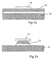
- Figure 1a shows a base plate, constituting a substrate 10, coated of a stack of layer 12 which, after different operations will form the laser waveguide, consisting of an active region and two coats taking this last sandwich.
- the following operation consists in depositing the layer electrically insulating 22, while maintaining the masking layer 14.
- This operation is carried out by depositing InP in the vapor phase, by a chemical process, from an organometallic compound, better known to those skilled in the art under the abbreviation of MOCVD abbreviation of English paraphrase “metal organic physical vapor deposition. "Such a process is described in a manner complete in “Materials Aspects of GaAs and InP Based Srtuctures "by V. Swaminathan and A. T. Macrander, Prentice Hall advanced reference series. ISBN 0-13-346826-7.
- the deposit is interrupted when the thickness of the layer 22, of InP, is equal to that of stacking 12.
- the doped InP substrate provides the lower electrode function. Also, in applying a voltage between the two electrodes, it is possible to inject a current in the stack, to cause the emission of coherent light.
- the structure of the stack can, of course, also include numerous configuration variants, for example those described in patent applications WO 99/00572 and FR 99 03845.
Landscapes
- Physics & Mathematics (AREA)
- Optics & Photonics (AREA)
- Chemical & Material Sciences (AREA)
- Engineering & Computer Science (AREA)
- Nanotechnology (AREA)
- Condensed Matter Physics & Semiconductors (AREA)
- General Physics & Mathematics (AREA)
- Electromagnetism (AREA)
- Life Sciences & Earth Sciences (AREA)
- Biophysics (AREA)
- Crystallography & Structural Chemistry (AREA)
- Semiconductor Lasers (AREA)
Claims (10)
- Halbleiterlaser mit Quantenkaskade mitdadurch gekennzeichnet, dass die elektrisch isolierende Schicht (22) die Seitenflächen gänzlich bedeckt, ohne über die obere Fläche hinauszuragen, und dass ihre Dicke zumindest gleich einem Drittel der Dicke des Stapels (12) ist.einem Substrat (10),einem Stapel (12) aus Schichten von prismatischer Form mit einem im Wesentlichen trapezförmigen Querschnitt, einer unteren Fläche die auf dem Substrat (10) angeordnet ist, einer oberen Fläche und Seitenflächen, wobei der Stapel einen Verstärkungsbereich bildet und zwei Ummantelungen, zwischen denen der Verstärkungsbereich eingeschoben ist,zwei Elektroden (10, 24), die auf beiden Seiten des Stapels (12) angeordnet sind, von denen eine (24) von einer Schicht aus elektrisch leitendem Material gebildet wird, die zumindest teilweise die Fläche des Stapels bedeckt, die dem Substrat gegenüberliegt, undeiner elektrisch isolierenden Schicht (22), die zwischen die zwei Elektroden eingeschoben ist,
- Laser nach Anspruch 1, dadurch gekennzeichnet, dass die elektrisch isolierende Schicht (22) das Substrat (10) zumindest in dem an den Stapel (12) angrenzenden Bereich bedeckt und eine Dicke aufweist, die zumindest gleich dieses letzteren ist.
- Laser nach Anspruch 2, dadurch gekennzeichnet, dass die Dicke der elektrisch isolierenden Schicht (22) im Wesentlichen gleich der Dicke des Stapels (12) ist.
- Laser nach Anspruch 3, dadurch gekennzeichnet, dass das Substrat (10) aus einem Halbleitermaterial ist, das dotiert ist, um es leitend zu machen.
- Laser nach Anspruch 4, dadurch gekennzeichnet, dass:das Substrat (10) von einer Platte aus mit Silizium dotierten Indiumphosphid (InP) besteht,die Ummantelungen jeweils von Schichten gebildet werden, die aus einer Legierung aus Indiumgalliumarsenid (InGaAs) und einer Legierung aus Indiumaluminiumarsenid gebildet sind,der aktive Bereich von einer Abfolge von Schichten aus Aluminiumindiumarsenid (AlInAs) und Aluminiumgaliumarsenid (AlGaAs) gebidet wird, und dassdie elektrisch isolierende Schicht (22) aus Indiumphosphid besteht.
- Laser nach Anspruch 5, dadurch gekennzeichnet, dass das Indiumphosphid, das die elektrisch isolierende Schicht (22) bildet, durch Dotierung mit Eisen von halbisolierender Art ist.
- Laser nach Anspruch 5, dadurch gekennzeichnet, dass das Indiumphosphid, das die elektrisch isolierende Schicht (22) bildet, nicht dotiert ist.
- Verfahren zur Herstellung eines Lasers nach einem der vorhergehenden Ansprüche, dadurch gekennzeichnet, dass es die folgenden Vorgänge umfasst:Aufbringen von Schichten, die dazu bestimmt sind, den Stapel (12) zu bilden,Aufbringen einer Maskierungschicht (14),Attackieren der Maskierungschicht (14) ausserhalb des Bereichs, der den Stapel bilden soll,Attackieren der Schichten, die den Stapel (12) bilden sollen, ausserhalb des maskierten Bereichs,Aufbringen einer elektrisch isolierenden Schicht (22) auf die nicht maskierten Abschnitte in der Gasphase durch ein chemisches Verfahren auf Basis einer metallorganischen Verbindung (MOCVD) bis eine Dicke erreicht ist, die im Wesentlichen gleich der Dicke des Stapels (12) ist,Beseitigung der Maskierungschicht (14) undAufbringen eine Leitungsschicht (24), die insbesondere den Stapel (12) auf seiner oberen Fläche bedeckt.
- Verfahren nach Anspruch 8, dadurch gekennzeichnet, dass der Vorgang des Aufbringens der elektrisch isolierenden Schicht (22) erfolgt, bis eine Dicke erreicht ist, die im Wesentlichen gleich der Dicke des Stapels (12) ist.
- Verfahren nach einem der Ansprüche 8 und 9, dadurch gekennzeichnet, dass die Maskierungschicht (14) aus SiO2 hergestellt wird.
Priority Applications (1)
| Application Number | Priority Date | Filing Date | Title |
|---|---|---|---|
| EP01905566A EP1262003B1 (de) | 2000-03-03 | 2001-02-26 | Quantumcascade-laser und sein herstellungsverfahren |
Applications Claiming Priority (4)
| Application Number | Priority Date | Filing Date | Title |
|---|---|---|---|
| EP00810183 | 2000-03-03 | ||
| EP00810183A EP1130724A1 (de) | 2000-03-03 | 2000-03-03 | Quantenkaskadierter Laser und sein Herstellungsverfahren |
| EP01905566A EP1262003B1 (de) | 2000-03-03 | 2001-02-26 | Quantumcascade-laser und sein herstellungsverfahren |
| PCT/CH2001/000123 WO2001065651A1 (fr) | 2000-03-03 | 2001-02-26 | Laser a cascade quantique et procede pour la fabrication d'un tel laser |
Publications (2)
| Publication Number | Publication Date |
|---|---|
| EP1262003A1 EP1262003A1 (de) | 2002-12-04 |
| EP1262003B1 true EP1262003B1 (de) | 2003-11-12 |
Family
ID=8174582
Family Applications (2)
| Application Number | Title | Priority Date | Filing Date |
|---|---|---|---|
| EP00810183A Withdrawn EP1130724A1 (de) | 2000-03-03 | 2000-03-03 | Quantenkaskadierter Laser und sein Herstellungsverfahren |
| EP01905566A Expired - Lifetime EP1262003B1 (de) | 2000-03-03 | 2001-02-26 | Quantumcascade-laser und sein herstellungsverfahren |
Family Applications Before (1)
| Application Number | Title | Priority Date | Filing Date |
|---|---|---|---|
| EP00810183A Withdrawn EP1130724A1 (de) | 2000-03-03 | 2000-03-03 | Quantenkaskadierter Laser und sein Herstellungsverfahren |
Country Status (5)
| Country | Link |
|---|---|
| US (2) | US6665325B2 (de) |
| EP (2) | EP1130724A1 (de) |
| JP (1) | JP2003526214A (de) |
| DE (1) | DE60101217T2 (de) |
| WO (1) | WO2001065651A1 (de) |
Families Citing this family (20)
| Publication number | Priority date | Publication date | Assignee | Title |
|---|---|---|---|---|
| US6449024B1 (en) | 1996-01-26 | 2002-09-10 | Semiconductor Energy Laboratory Co., Inc. | Liquid crystal electro-optical device utilizing a polymer with an anisotropic refractive index |
| EP1283571B1 (de) | 2001-08-06 | 2015-01-14 | nanoplus GmbH Nanosystems and Technologies | Laser mit schwach gekoppeltem Gitterbereich |
| EP1343232B1 (de) * | 2002-03-08 | 2007-05-02 | nanoplus GmbH Nanosystems and Technologies | Ein Halbleiterlaserarray mit seitlicher Gratingstruktur |
| US7301977B2 (en) * | 2004-06-10 | 2007-11-27 | Nanoplus Gmbh | Tuneable unipolar lasers |
| US7274719B2 (en) * | 2005-03-09 | 2007-09-25 | Agilent Technologies, Inc. | Buried heterostructure quantum cascade laser |
| US7403552B2 (en) * | 2006-03-10 | 2008-07-22 | Wisconsin Alumni Research Foundation | High efficiency intersubband semiconductor lasers |
| JP2008218915A (ja) * | 2007-03-07 | 2008-09-18 | Hamamatsu Photonics Kk | 量子カスケードレーザ素子 |
| JP5355599B2 (ja) | 2011-01-19 | 2013-11-27 | 株式会社東芝 | 半導体発光装置およびその製造方法 |
| JP5729138B2 (ja) * | 2011-05-30 | 2015-06-03 | 住友電気工業株式会社 | 光半導体デバイスの製造方法 |
| JP5803366B2 (ja) * | 2011-07-14 | 2015-11-04 | 住友電気工業株式会社 | 埋め込みヘテロ構造半導体レーザの製造方法及び埋め込みヘテロ構造半導体レーザ |
| JP2013149665A (ja) | 2012-01-17 | 2013-08-01 | Sumitomo Electric Ind Ltd | 量子カスケード半導体レーザ |
| JP2013254907A (ja) * | 2012-06-08 | 2013-12-19 | Sumitomo Electric Ind Ltd | 量子カスケード半導体レーザ |
| JP2014229744A (ja) * | 2013-05-22 | 2014-12-08 | 住友電気工業株式会社 | 半導体発光組立体 |
| JP6467193B2 (ja) * | 2014-10-30 | 2019-02-06 | 浜松ホトニクス株式会社 | 量子カスケードレーザ |
| KR101984163B1 (ko) * | 2014-12-03 | 2019-05-30 | 알페스 라제르스 에스아 | 전류 차단층을 가진 양자 폭포 레이저 |
| US10038307B2 (en) * | 2014-12-19 | 2018-07-31 | Alpes Lasers Sa | Quantum cascade laser optimized for epitaxial side-down mounting |
| JP6464895B2 (ja) | 2015-04-03 | 2019-02-06 | 住友電気工業株式会社 | 量子カスケード半導体レーザ |
| JP2016197657A (ja) | 2015-04-03 | 2016-11-24 | 住友電気工業株式会社 | 量子カスケード半導体レーザ |
| JP2017157865A (ja) * | 2017-06-07 | 2017-09-07 | 株式会社東芝 | 半導体発光装置およびその製造方法 |
| CN118117442B (zh) * | 2024-02-02 | 2024-11-22 | 江西杰创半导体有限公司 | Vcsel器件的制作方法及vcsel器件 |
Family Cites Families (18)
| Publication number | Priority date | Publication date | Assignee | Title |
|---|---|---|---|---|
| JPS62166586A (ja) * | 1986-01-20 | 1987-07-23 | Nec Corp | 半導体発光素子とその製造方法 |
| JP2747080B2 (ja) * | 1990-03-26 | 1998-05-06 | 松下電器産業株式会社 | 半導体レーザ装置およびその製造方法 |
| US5214662A (en) * | 1990-11-16 | 1993-05-25 | Furukawa Electric Co., Ltd. | Semiconductor optical devices with pn current blocking layers of wide-band gap materials |
| JP2814786B2 (ja) * | 1991-10-08 | 1998-10-27 | 日本電気株式会社 | 半導体レーザ |
| US5416790A (en) * | 1992-11-06 | 1995-05-16 | Sanyo Electric Co., Ltd. | Semiconductor laser with a self-sustained pulsation |
| DE4314498A1 (de) * | 1993-05-03 | 1994-11-10 | Bayer Ag | Verfahren zur Herstellung von Perfluoralkoxy(alkylthio)-benzolen |
| JPH07193333A (ja) * | 1993-12-27 | 1995-07-28 | Mitsubishi Chem Corp | 半導体発光素子 |
| US5400354A (en) * | 1994-02-08 | 1995-03-21 | Ludowise; Michael | Laminated upper cladding structure for a light-emitting device |
| JPH07254750A (ja) * | 1994-03-15 | 1995-10-03 | Toshiba Corp | 半導体レーザ |
| US5789772A (en) * | 1994-07-15 | 1998-08-04 | The Whitaker Corporation | Semi-insulating surface light emitting devices |
| JPH09331110A (ja) * | 1996-06-12 | 1997-12-22 | Mitsubishi Electric Corp | 光半導体装置、および光半導体装置の製造方法 |
| JP3684519B2 (ja) * | 1996-08-20 | 2005-08-17 | 富士通株式会社 | 半導体レーザの製造方法 |
| US5789722A (en) * | 1996-11-12 | 1998-08-04 | Zimac Laboratories, Inc. | Modular multizone heater system and method |
| GB9704987D0 (en) * | 1997-03-11 | 1997-04-30 | Isis Innovation | Infrared radiation source |
| JPH11121860A (ja) * | 1997-10-20 | 1999-04-30 | Oki Electric Ind Co Ltd | 化合物半導体発光素子およびその形成方法 |
| US6137817A (en) * | 1998-06-12 | 2000-10-24 | Lucent Technologies Inc. | Quantum cascade laser |
| US6556605B1 (en) * | 2000-02-29 | 2003-04-29 | Triquent Technology Holding, Co. | Method and device for preventing zinc/iron interaction in a semiconductor laser |
| US6463088B1 (en) * | 2000-07-07 | 2002-10-08 | Lucent Technologies Inc. | Mesa geometry semiconductor light emitter having chalcogenide dielectric coating |
-
2000
- 2000-03-03 EP EP00810183A patent/EP1130724A1/de not_active Withdrawn
-
2001
- 2001-02-26 EP EP01905566A patent/EP1262003B1/de not_active Expired - Lifetime
- 2001-02-26 JP JP2001564428A patent/JP2003526214A/ja active Pending
- 2001-02-26 DE DE60101217T patent/DE60101217T2/de not_active Expired - Lifetime
- 2001-02-26 US US10/220,099 patent/US6665325B2/en not_active Expired - Lifetime
- 2001-02-26 WO PCT/CH2001/000123 patent/WO2001065651A1/fr not_active Ceased
-
2003
- 2003-12-15 US US10/736,488 patent/US20040126912A1/en not_active Abandoned
Also Published As
| Publication number | Publication date |
|---|---|
| US20040126912A1 (en) | 2004-07-01 |
| EP1262003A1 (de) | 2002-12-04 |
| US6665325B2 (en) | 2003-12-16 |
| EP1130724A1 (de) | 2001-09-05 |
| WO2001065651A1 (fr) | 2001-09-07 |
| DE60101217T2 (de) | 2004-09-09 |
| DE60101217D1 (de) | 2003-12-18 |
| JP2003526214A (ja) | 2003-09-02 |
| US20030021315A1 (en) | 2003-01-30 |
Similar Documents
| Publication | Publication Date | Title |
|---|---|---|
| EP1262003B1 (de) | Quantumcascade-laser und sein herstellungsverfahren | |
| EP0829934B1 (de) | Herstellungsverfahren einer optoelektrischen Halbleitervorrichtung, und Vorrichtung oder Matrix von Vorrichtungen hergestellt unter Verwendung dieses Verfahrens | |
| EP3168946B1 (de) | Laservorrichtung und herstellungsverfahren einer solchen laservorrichtung | |
| EP3352312B1 (de) | Photonische vorrichtung, die einen laser umfasst, der optisch mit einem silizium-wellenleiter verbunden ist, und herstellungsverfahren einer solchen photonischen vorrichtung | |
| EP0765014B1 (de) | Oberflächenemittierender Laser mit vertikalem Resonator mit einer Wellenlänge zwischen 1,3 und 1,5 Mikrometer sowie dessen Herstellung | |
| FR2690278A1 (fr) | Composant photovoltaïque multispectral à empilement de cellules, et procédé de réalisation. | |
| FR2695261A1 (fr) | Laser émetteur en surface et son procédé de fabrication. | |
| FR2727791A1 (fr) | Dispositif a semi-conducteur optique et procede de fabrication de celui-ci | |
| EP0617839B1 (de) | Verfahren zur Herstellung von Halbleiterkomponenten, insbesondere auf GaAs oder InP, bei dem das Substrat auf chemischem Wege wiedergewonnen wird | |
| FR2761811A1 (fr) | Technologie sans gravure pour integration de composants | |
| FR2967813A1 (fr) | Procédé de réalisation d'une structure a couche métallique enterrée | |
| FR2690286A1 (fr) | Cavité laser à hétérostructure semi-conductrice dissymétrique et laser équipé de cette cavité. | |
| EP0817337B1 (de) | Herstellungsverfahren für einen Oberflächenemittierenden Laser | |
| EP2504895B1 (de) | Lasersystem, heterostruktur und aktive zone mit gekoppelten sub-quantentöpfen, erzeugung einer laserstrahlung von 1.55 mikrometern | |
| EP1470622B1 (de) | Sättigbares absorberbauteil und verfahren zu dessen herstellung | |
| EP0494013A1 (de) | Herstellungsverfahren für oberflächenemittierende Halbleiterlaser und damit hergestellte Laser | |
| WO2004097945A1 (fr) | Procede de realisation d'un dispositif semi-conducteur a metallisations auto-alignees. | |
| FR2743197A1 (fr) | Dispositif a semi-conducteur a structure mesa et procede de fabrication d'un tel dispositif | |
| FR2701574A1 (fr) | Modulateur semi-conducteur d'intensité de lumière. | |
| EP1670066A1 (de) | Herstellungsverfahren für eine integrierte Schaltung mit eingebettetem Spiegel und entsprechende Schaltung | |
| EP0506557B1 (de) | Herstellungsverfahren für einen Halbleiterlaser mit vergrabener Streifenstruktur | |
| EP4481961B1 (de) | Optoelektronisches bauelement mit vergrabener spitze mit hoher leistung | |
| EP0498695B1 (de) | Verfahren zum Herstellen eines planaren Halbleiterlasers mit vergrabener Streifenstruktur | |
| EP0617841B1 (de) | Verfahren zur Herstellung von Halbleiterkomponenten, bei dem das Substrat auf elektrochemischem Wege wiedergewonnen wird | |
| FR3164872A1 (fr) | Structure de support et dispositif optoélectronique |
Legal Events
| Date | Code | Title | Description |
|---|---|---|---|
| PUAI | Public reference made under article 153(3) epc to a published international application that has entered the european phase |
Free format text: ORIGINAL CODE: 0009012 |
|
| 17P | Request for examination filed |
Effective date: 20020904 |
|
| AK | Designated contracting states |
Kind code of ref document: A1 Designated state(s): AT BE CH CY DE DK ES FI FR GB GR IE IT LI LU MC NL PT SE TR |
|
| RIN1 | Information on inventor provided before grant (corrected) |
Inventor name: MULLER, ANTOINE Inventor name: BECK, MATTIAS Inventor name: FAIST,JEROME |
|
| GRAH | Despatch of communication of intention to grant a patent |
Free format text: ORIGINAL CODE: EPIDOS IGRA |
|
| GRAS | Grant fee paid |
Free format text: ORIGINAL CODE: EPIDOSNIGR3 |
|
| GRAA | (expected) grant |
Free format text: ORIGINAL CODE: 0009210 |
|
| AK | Designated contracting states |
Kind code of ref document: B1 Designated state(s): CH DE FR GB LI |
|
| REG | Reference to a national code |
Ref country code: GB Ref legal event code: FG4D Free format text: NOT ENGLISH |
|
| REG | Reference to a national code |
Ref country code: CH Ref legal event code: EP |
|
| REF | Corresponds to: |
Ref document number: 60101217 Country of ref document: DE Date of ref document: 20031218 Kind code of ref document: P |
|
| REG | Reference to a national code |
Ref country code: IE Ref legal event code: FG4D Free format text: FRENCH |
|
| REG | Reference to a national code |
Ref country code: CH Ref legal event code: NV Representative=s name: GLN GRESSET & LAESSER NEUCHATEL CABINET DE CONSEIL |
|
| GBT | Gb: translation of ep patent filed (gb section 77(6)(a)/1977) |
Effective date: 20040211 |
|
| REG | Reference to a national code |
Ref country code: IE Ref legal event code: FD4D |
|
| PLBE | No opposition filed within time limit |
Free format text: ORIGINAL CODE: 0009261 |
|
| STAA | Information on the status of an ep patent application or granted ep patent |
Free format text: STATUS: NO OPPOSITION FILED WITHIN TIME LIMIT |
|
| 26N | No opposition filed |
Effective date: 20040813 |
|
| PG25 | Lapsed in a contracting state [announced via postgrant information from national office to epo] |
Ref country code: FR Free format text: LAPSE BECAUSE OF NON-PAYMENT OF DUE FEES Effective date: 20051031 |
|
| REG | Reference to a national code |
Ref country code: FR Ref legal event code: ST Effective date: 20051031 |
|
| REG | Reference to a national code |
Ref country code: FR Ref legal event code: D3 |
|
| REG | Reference to a national code |
Ref country code: CH Ref legal event code: PFA Owner name: ALPES LASERS S.A., CH Free format text: FORMER OWNER: ALPES LASERS S.A., CH |
|
| REG | Reference to a national code |
Ref country code: FR Ref legal event code: PLFP Year of fee payment: 16 |
|
| REG | Reference to a national code |
Ref country code: CH Ref legal event code: PFA Owner name: ALPES LASERS S.A., CH Free format text: FORMER OWNER: ALPES LASERS S.A., CH |
|
| REG | Reference to a national code |
Ref country code: FR Ref legal event code: PLFP Year of fee payment: 17 |
|
| REG | Reference to a national code |
Ref country code: FR Ref legal event code: PLFP Year of fee payment: 18 |
|
| REG | Reference to a national code |
Ref country code: CH Ref legal event code: NV Representative=s name: BOVARD SA NEUCHATEL CONSEILS EN PROPRIETE INTE, CH |
|
| REG | Reference to a national code |
Ref country code: CH Ref legal event code: NV Representative=s name: ABACUS PATENTANWAELTE KLOCKE SPAETH BARTH, CH |
|
| PG25 | Lapsed in a contracting state [announced via postgrant information from national office to epo] |
Ref country code: FR Free format text: LAPSE BECAUSE OF NON-PAYMENT OF DUE FEES Effective date: 20051031 |
|
| PGRI | Patent reinstated in contracting state [announced from national office to epo] |
Ref country code: FR Effective date: 20060203 |
|
| PGFP | Annual fee paid to national office [announced via postgrant information from national office to epo] |
Ref country code: DE Payment date: 20191212 Year of fee payment: 20 Ref country code: GB Payment date: 20200219 Year of fee payment: 20 |
|
| PGFP | Annual fee paid to national office [announced via postgrant information from national office to epo] |
Ref country code: FR Payment date: 20200219 Year of fee payment: 20 |
|
| PGFP | Annual fee paid to national office [announced via postgrant information from national office to epo] |
Ref country code: CH Payment date: 20200427 Year of fee payment: 20 |
|
| REG | Reference to a national code |
Ref country code: DE Ref legal event code: R071 Ref document number: 60101217 Country of ref document: DE |
|
| REG | Reference to a national code |
Ref country code: CH Ref legal event code: PL |
|
| REG | Reference to a national code |
Ref country code: GB Ref legal event code: PE20 Expiry date: 20210225 |
|
| PG25 | Lapsed in a contracting state [announced via postgrant information from national office to epo] |
Ref country code: GB Free format text: LAPSE BECAUSE OF EXPIRATION OF PROTECTION Effective date: 20210225 |