EP1263135A2 - Duales System zur bidirektionalen Verschwendung von Oberwellen - Google Patents
Duales System zur bidirektionalen Verschwendung von Oberwellen Download PDFInfo
- Publication number
- EP1263135A2 EP1263135A2 EP02252527A EP02252527A EP1263135A2 EP 1263135 A2 EP1263135 A2 EP 1263135A2 EP 02252527 A EP02252527 A EP 02252527A EP 02252527 A EP02252527 A EP 02252527A EP 1263135 A2 EP1263135 A2 EP 1263135A2
- Authority
- EP
- European Patent Office
- Prior art keywords
- filter
- pass filter
- low pass
- high pass
- output
- Prior art date
- Legal status (The legal status is an assumption and is not a legal conclusion. Google has not performed a legal analysis and makes no representation as to the accuracy of the status listed.)
- Withdrawn
Links
Images

Classifications
-
- H—ELECTRICITY
- H03—ELECTRONIC CIRCUITRY
- H03H—IMPEDANCE NETWORKS, e.g. RESONANT CIRCUITS; RESONATORS
- H03H7/00—Multiple-port networks comprising only passive electrical elements as network components
- H03H7/01—Frequency selective two-port networks
- H03H7/06—Frequency selective two-port networks including resistors
- H03H7/07—Bridged T-filters
-
- H—ELECTRICITY
- H01—ELECTRIC ELEMENTS
- H01J—ELECTRIC DISCHARGE TUBES OR DISCHARGE LAMPS
- H01J37/00—Discharge tubes with provision for introducing objects or material to be exposed to the discharge, e.g. for the purpose of examination or processing thereof
- H01J37/32—Gas-filled discharge tubes
- H01J37/32009—Arrangements for generation of plasma specially adapted for examination or treatment of objects, e.g. plasma sources
- H01J37/32082—Radio frequency generated discharge
- H01J37/32174—Circuits specially adapted for controlling the RF discharge
-
- H—ELECTRICITY
- H01—ELECTRIC ELEMENTS
- H01J—ELECTRIC DISCHARGE TUBES OR DISCHARGE LAMPS
- H01J37/00—Discharge tubes with provision for introducing objects or material to be exposed to the discharge, e.g. for the purpose of examination or processing thereof
- H01J37/32—Gas-filled discharge tubes
- H01J37/32009—Arrangements for generation of plasma specially adapted for examination or treatment of objects, e.g. plasma sources
- H01J37/32082—Radio frequency generated discharge
-
- H—ELECTRICITY
- H03—ELECTRONIC CIRCUITRY
- H03H—IMPEDANCE NETWORKS, e.g. RESONANT CIRCUITS; RESONATORS
- H03H7/00—Multiple-port networks comprising only passive electrical elements as network components
- H03H7/01—Frequency selective two-port networks
- H03H7/0115—Frequency selective two-port networks comprising only inductors and capacitors
-
- H—ELECTRICITY
- H03—ELECTRONIC CIRCUITRY
- H03H—IMPEDANCE NETWORKS, e.g. RESONANT CIRCUITS; RESONATORS
- H03H7/00—Multiple-port networks comprising only passive electrical elements as network components
- H03H7/01—Frequency selective two-port networks
- H03H7/17—Structural details of sub-circuits of frequency selective networks
- H03H7/1741—Comprising typical LC combinations, irrespective of presence and location of additional resistors
- H03H7/1766—Parallel LC in series path
Definitions
- This invention relates to high power RF amplifier systems, such as those employed in semiconductor plasma processing applications.
- Plasma processing installations which includes plasma reactors, are in widespread use in semiconductor fabrication.
- Plasma reactors are used to change the electrical characteristics of raw materials (e.g. silicon) during the manufacture of semiconductor-based electrical components like discrete transistors, medium and large scale integrated circuits, microprocessors and random-access memories.
- Typical operations performed using plasma reactors include sputtering, plasma etching, plasma deposition, and reactive ion etching.
- a semiconductor work-piece is placed in the reactor.
- gas is introduced into the plasma reactor at low pressure.
- radio frequency (RF) power is applied to the gas to convert the gas into a plasma.
- the plasma is comprised of electrically-charged ions that react with exposed regions of the semiconductor work-piece.
- Plasma processing installations used in semiconductor fabrication generally comprise an RF generator, an RF power cable coupled at one end to the RF generator, an impedance matching network, and a RF power cable or a pair of copper straps which connect to the electrodes of the plasma reactor.
- the impedance of the plasma reactor is subject to substantial variation. Prior to ignition, the gas in the reactor is not ionized and therefore not conductive. Upon application of RF power, the gas begins to ionize and the load impedance drops as charge carriers are created in the reactor. After the start-up period a steady-state operating condition is eventually achieved.
- Variations in the plasma flux can also cause significant transients in the load impedance, even during steady-state operations.
- substantial impedance variations encountered may lead to significant power being reflected back to the RF generator causing it to become unstable and possibly destabilize the plasma process or damage the RF generator. This is especially the case for high "Q" plasma processes.
- standard non-dissipative filter configurations are not sufficient for the stable operation of the entire range of processes encountered.
- the process is driven by radio frequency energy typically provided at a relatively constant frequency, or band of frequencies such as for instance 13.56 MHz, ⁇ 5%, at levels up to several kilowatts.
- radio frequency energy typically provided at a relatively constant frequency, or band of frequencies such as for instance 13.56 MHz, ⁇ 5%, at levels up to several kilowatts.
- An RF energy delivery system may comprise an RF generator, a matching network, and a load.
- Frequency agile plasma systems which operate over a pre-determined frequency bandwidth instead of a constant frequency, for instance a bandwidth representing a fluctuation of between about ⁇ 5 to ⁇ 10%, are becoming generally more desirable as they allow greater freedom to accomplish optimal plasma impedance match and thus allow a fixed or variable matching network.
- the application of RF energy by the RF generator to the plasma chamber produces out of band energy which can be at multiples of the source frequency (harmonics) or at fractions thereof (sub-harmonics).
- Dissipative filters have often been employed in communications work, for example, as a narrow bandpass I.F. filter after the first down converter of a receiver front end. Dissipative filters are employed to improve performance, where it is needed to provide proper controlled termination to the out of band signals.
- dissipative filters have not been favored because they do not offer the sharp attenuation slope of an equivalent lossless filter. Consequently, because of the shallow attenuation slope and energy dissipation problems, circuit designers have been reluctant to interpose filters of this type in an RF delivery system where the RF power can be several kilowatts.
- a dissipative harmonic filter can be interposed in between the generator and the matching network to deal with the problem of out-of-band signals generated by the non-linearity of the plasma load as described in U.S. Patent No. 5,187,457.
- Previous attempts to do this have generally involved reflective type lossless filters, which reflect rather than absorb harmonics. This, however, did not solve plasma chamber stability problems associated with specific process conditions, specifically high "Q" recipes, because standard reflective filters with both Chebyshev or elliptic designs do not provide dissipative termination of harmonics. While these designs keep harmonics from the load, they ground harmonics via alternative paths. The harmonics in the ground paths create harmonic ground currents, known as "hot grounds" which create additional gate-source voltage differential, potentially harmful to MOSFET dies.
- a diplexer with a terminated high pass filter at the input of the low pass filter may also be interposed between the driver output and amplifier input inside the RF generator.
- Cascading filters such as those referenced in U.S. Patent No. 5,187,457, are dissipative, yet are only suitable for fixed frequency plasma systems because of excessive power loss over the required bandwidth, removal of dissipated power and the associated size. Moreover, these filters lack sufficient rejection of the harmonics and so, in addition, require lossless filters for the desired plasma system harmonic rejection levels.
- high voltage MOSFETs are sensitive to harmonic ground currents caused by switchmode driver output and energy reflected back from the plasma chamber. The occurrence of ground harmonic currents may cause the RF power amplifier to: a) switch inconsistently for the desired performance with respect to power gain and efficiency; b) become unstable and deliver incorrect power with respect to set point; c) cause plasma flux drop-out; and, d) increase gate-source differential voltages causing damage to the MOSFET dies.
- the present invention is directed to a dual directional diplexer harmonics dissipation filter for a RF generator system which includes an input terminal coupled to a power source providing a radio frequency signal in a predetermined frequency range, an output terminal for providing the radio frequency signal to a load at the predetermined frequency range, a low pass filter having an input and output, the low pass filter connected between the input terminal and the output terminal, a plurality of high pass filters coupled to the low pass filter wherein the plurality of high pass filters dissipate signals in excess of the predetermined frequency range and the plurality of high pass filters have a predetermined circuitry effect selected from the group consisting of capacitance and inductance, and the resultant effect is offset and absorbed by the low pass filter at the input and the output.
- a dual directional harmonics dissipation filter for a frequency agile RF generator system powering a load, comprising an RF power amplifier, an output terminal coupled to the RF power amplifier providing a radio frequency signal in a predetermined frequency range, a low pass filter having an input and an output, an input impedance and an output impedance, the low pass filter coupled to the output terminal, a high pass filter coupled to the low pass filter output wherein the high pass filter receives and dissipates harmonic signals reflected from the load in excess of the predetermined frequency band and wherein the high pass filter's effects on the output impedance of the low pass filter is offset, and filter means for managing harmonic signals produced by the RF power amplifier, the filter means coupled to the low pass filter input wherein the filter means' effects on the input impedance of the low pass filter is offset.
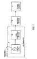
- one embodiment of a system for employing high-power radio frequency (RF) energy comprises an RF generator 9 having an RF power amplifier 10 and a dual directional diplexer 16.
- the RF power amplifier 10 providing alternating current within a radio frequency band, for instance ⁇ 5 to ⁇ 10% of 13.56 MHz, at a power of up to 3000 watts for this example.
- the RF power amplifier 10 has an effective output impedance of 50 ohms.
- the RF energy is applied to a plasma chamber 12, which imposes an RF load.
- the load impedance can vary during operation, and is non-linear, thereby converting the frequencies of the input RF energy within the preferred frequency band into energy at frequencies which are multiples or fractions of that input frequency.
- impedance matching network 14 is interposed between a dual directional diplexer 16 and plasma chamber load 12 for matching the impedance of the plasma chamber 12 to the 50 ohm impedance of the RF power amplifier 10.
- the dual directional diplexer 16 in accordance with the present invention is preferably placed in series with the RF power amplifier 10 and the matching network 14 for passing energy in a passband, for instance, within ⁇ 5% centered on the 13.56 MHz frequency, but dissipating energy that is above the passband.
- the low frequency and subharmoic energy below the passband is dissipated in resistive terminations via other filter networks, not pictured, in the RF power amplifier 10.
- the dual directional diplexer 16 is illustrated here as being in series between the RF power amplifier 10 and the matching network 14, but it is contemplated that it may also be placed in other suitable locations in the system, e.g. within the RF power generator 9. Given the relatively smaller size of its circuitry, this and other options for placement of the dual directional diplexer 16 within the system are possible.
- FIG. 2 is a block diagram illustrating the system components of the dual directional diplexer 16.
- the dual directional diplexer 16 includes low pass filter 20 which receives output 25 from RF power amplifier 10 and at least two high pass filters 27a and 27b to receive and dissipate harmonic energy.
- diplexer 16 through which the RF power amplifier 10 output 25 passes includes a fifth order 0.1 dB passband ripple elliptic response low pass filter 20 and a plurality of fifth order 0.1dB passband ripple Chebyshev response high pass filters.
- high pass filters 27a and 27b are pictured.
- Low pass filter 20 has a cutoff frequency of 16.4 MHz, with a typical rejection floor of -43dBc. Second harmonic rejection from this filter is typically -42 dBc. The third harmonic rejection is typically -62 dBc.
- the rejection of harmonics by low pass filter 20 is not enough, and steps must be taken to dissipate the harmonics energy.
- dissipative termination of harmonics is achieved through at least two high pass filters, 27a and 27b, one added at a junction 15 prior to the input and one added at a junction 17 after the output of the low pass filter 20.
- Harmonic energy may enter the system in one of two ways. It may be produced by the RF power amplifier 10 or it may be reflected back from the plasma chamber 12 during the transient flux produced by ionization of the plasma medium. Dissipation of harmonics from the RF power amplifier 10 is provided by the high pass filter 27a at the low pass filter 20 input. Dissipation of harmonics reflected back from the plasma chamber 12, coming back toward the RF power amplifier 10, is received by the high pass filter 27b and dissipated.
- the diplexer 16 i.e., high pass/low pass filter arrangement, typically minimizes harmonic distortion and has a dissipative harmonic termination for harmonics received at the high pass filters' 27a and 27b inputs.
- the low pass/high pass filter combination of the present embodiment forms a dual directional diplexer 16 dissipating harmonic energy originating from both the RF power amplifier output and that reflected back from the plasma chamber load.
- dual directional harmonic filter arrangements including high pass and low pass filters, are contemplated and are within the scope of this invention.
- more than two high pass filters may be utilized to increase dissipation of harmonic energy with or without additional low pass filters.
- use of only one high pass filter, connected at a junction between the low pass filter output and the load, to dissipate energy reflected back from the plasma chamber, may be employed in conjunction with other means for managing, e.g. dissipating, reflecting and/or grounding, harmonic energy produced from the RF power amplifier.
- the single high pass filter at the low pass filter output may be used without a second high pass filter at the low pass filter input, but rather with a diplexer, reflective type filter or cascading dissipative filter, located, for instance, elsewhere within the RF generator circuitry, such as incorporated into RF power amplifier circuitry, or as a separate harmonics filter circuitry in series between the RF generator and the matching network to provide reflection, dissipation or grounding of harmonics produced by the RF generator during operation.
- a diplexer, reflective type filter or cascading dissipative filter located, for instance, elsewhere within the RF generator circuitry, such as incorporated into RF power amplifier circuitry, or as a separate harmonics filter circuitry in series between the RF generator and the matching network to provide reflection, dissipation or grounding of harmonics produced by the RF generator during operation.
- the harmonics from the RF power amplifier and/or the plasma chamber are dissipated in the high pass filters' 27a and 27b resistive terminations without appreciably affecting the signal that is within the bandwidth, for instance between ⁇ 5% of 13.56 MHz, for frequency agile plasma systems.
- High pass filters 27a and 27b reduce the harmonic ground current and thus protect the RF generator from becoming unstable and/or delivering RF power to the plasma chamber 12 at a level much lower than at the set point and thereby causing flux drop-out in the plasma.
- the lower level of harmonic ground currents also protect the MOSFET dies in the power source from excessive gate-source voltage differential, typically not to exceed the ⁇ 30 volts specification limits.
- the presently preferred dual directional diplexer 16 provides stable operation of the RF power amplifier 10 over the entire range of voltage standing wave ratios (VSWRs) and over the complete dynamic range of the system. This is particularly important for the stability of plasma systems performing high "Q" processes.
- VSWRs voltage standing wave ratios
- the high pass filters 27a and 27b in the preferred embodiment have a fifth order, 0.1 dB passband ripple, Chebyshev response and dissipate up to about 500 watts of power.
- the cutoff frequency of the high pass filters is 23.2 MHz with a 3 dB point at 20.4 MHz.
- higher order filters e.g. seventh or ninth order filters, may also be used. While higher order filters will have less effect on the impedance and frequency response of the associated low pass filter, the increase in circuitry size is appreciable.
- Other specifications for the high pass filters applicable to the processes described herein will occur to those skilled in the art.
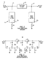
- the high pass filters 27a and 27b and low pass filter 20 are shown in more detail in the schematic diagram of Fig. 3, in which the low pass filter 20 may be tuned to a bandwidth between ⁇ 5% of 13.56 MHz.
- the low pass filter 20 may be of an elliptical design having capacitors C1, C3, and C5 shorting out-of-band higher frequencies, and parallel LC resonance paths A and B having inductors L1 and L2 as well as capacitors C2 and C4, blocking out-of-band higher frequencies, and passing the amplified clean RF signal at 13.56 MHz and over the, for instance, ⁇ 5% bandwidth. While illustrated as an elliptic design in Figure 3, the low pass filter 20 may also employ a Chebyshev design having shunt input-output capacitance or series input-output inductance topology.
- the high pass filters 27a and 27b are each made up of a series of capacitors, respectively, C6, C7, and C8, and C9, C10 and C11 appearing as shorts to higher frequencies (harmonics) and as opens, blocking low frequency currents from reaching the termination resistors, R1 and R2. Inductances L3 and L4 as well as L5 and L6 appear as shorts to lower frequencies and opens to higher frequencies.
- the bypassed higher frequency components which include 2nd, 3rd, 4th, 5th, etc. harmonics, are preferably consigned to a 50 Ohm dissipating resistance, R1 and R2. Frequencies lower than the predetermined band fall within the high pass filters' 27a and 27b reject bands.
- the high pass filters 27a and 27b each have a capacitance input, represented, respectively, by capacitors C6 and C9. While the high pass filters 27a and 27b in Figure 3 are Chebyshev in design, it is also contemplated that these may also be elliptic in design.
- the low pass filter 20 includes a capacitive input and output, respectively, C1 and C5, complementing the capacitive inputs of the high pass filters 27a and 27b in the reject band. The invention, therefore, contemplates offset, by the low pass filter's 20 input and output circuitry, of the capacitative effects of the high pass filters 27a and 27b on impedance to regain performance within the desired fundamental frequency band.
- the selected high pass filter topology (using series input capacitors) has capacitive input impedance in the reject band, resulting in an equivalent capacitance value in the predetermined frequency band, e.g. a bandwidth of ⁇ 5% 13.56MHz.
- This equivalent input capacitance of the high pass filters 27a and 27b can be offset by lowering the value of the low pass filter 20 input-output capacitance so that the high pass filter equivalent input capacitance is absorbed by the low pass filter. Proper offset of this equivalent input capacitance at both input-output terminals of the low pass filter 20 results in regaining the desired input-output impedances and frequency response.
- FIG. 4 illustrates an alternative embodiment of the invention.
- the low pass filter 100 uses inductance input L1 and inductance output L3, along with inductances L2, L4 and L5 and capacitors C1 and C2.
- High pass filters 200 and 300 employ inductance inputs L6 and L9, as well as inductances L7, L8 and L10 and L11, in series with capacitors C3 and C4 as well as C5 and C6, terminating in resistances R1 an R2 each having 50 ohms resistance values, for harmonic dissipation.
- the high pass filters 200 and 300 may have equivalent inductance values at their input ports. This inductance effect can be offset and absorbed by the inductive input and output ports series input inductance of the low pass filter 20 by adjusting inductance values at the low pass filter 20 input and output.
- this harmonic filter can be matched to an impedance other than 50 ohms, if appropriate.
- the dual directional diplexer can also be employed in other high-power, high frequency applications where a non-linear source drives a linear or non-linear load with high VSWR.
Landscapes
- Engineering & Computer Science (AREA)
- Physics & Mathematics (AREA)
- Plasma & Fusion (AREA)
- Chemical & Material Sciences (AREA)
- Analytical Chemistry (AREA)
- Power Engineering (AREA)
- Amplifiers (AREA)
- Filters And Equalizers (AREA)
Applications Claiming Priority (2)
| Application Number | Priority Date | Filing Date | Title |
|---|---|---|---|
| US09/832,476 US6587019B2 (en) | 2001-04-11 | 2001-04-11 | Dual directional harmonics dissipation system |
| US832476 | 2001-04-11 |
Publications (2)
| Publication Number | Publication Date |
|---|---|
| EP1263135A2 true EP1263135A2 (de) | 2002-12-04 |
| EP1263135A3 EP1263135A3 (de) | 2004-08-04 |
Family
ID=25261762
Family Applications (1)
| Application Number | Title | Priority Date | Filing Date |
|---|---|---|---|
| EP02252527A Withdrawn EP1263135A3 (de) | 2001-04-11 | 2002-04-09 | Duales System zur bidirektionalen Verschwendung von Oberwellen |
Country Status (5)
| Country | Link |
|---|---|
| US (1) | US6587019B2 (de) |
| EP (1) | EP1263135A3 (de) |
| JP (1) | JP2003008384A (de) |
| KR (1) | KR20020080260A (de) |
| CN (1) | CN1384604A (de) |
Families Citing this family (34)
| Publication number | Priority date | Publication date | Assignee | Title |
|---|---|---|---|---|
| DE10111151B4 (de) * | 2001-03-08 | 2007-10-18 | Vacuumschmelze Gmbh & Co. Kg | Filteranordnung |
| KR100377928B1 (ko) * | 2001-05-11 | 2003-03-29 | 삼성전자주식회사 | 이동 통신단말기에 장착된 근거리 무선 통신장치에서의신호간섭 제거방법 및 장치 |
| US6873225B2 (en) * | 2003-04-15 | 2005-03-29 | Microphase Corporation | Diplexers with low pass filter having distributed and non-distributed (lumped) elements |
| US20070099590A1 (en) * | 2003-12-25 | 2007-05-03 | Advantest Corporation | Frequency converter |
| FI119079B (fi) * | 2004-11-08 | 2008-07-15 | Elektrobit System Test Oy | Sähkölaitteen sähköisen piirin karakterisointi |
| US7780814B2 (en) * | 2005-07-08 | 2010-08-24 | Applied Materials, Inc. | Wafer pre-clean reactor cable termination for selective suppression/reflection of source and bias frequency cross products |
| CN100362619C (zh) * | 2005-08-05 | 2008-01-16 | 中微半导体设备(上海)有限公司 | 真空反应室的射频匹配耦合网络及其配置方法 |
| CN101297480B (zh) * | 2005-10-31 | 2012-08-08 | Mks仪器股份有限公司 | 用于向动态负载传递功率的系统和方法 |
| EP1837893A1 (de) * | 2006-03-25 | 2007-09-26 | HÜTTINGER Elektronik GmbH + Co. KG | Messeeinrichtung eines HF-Plasmasystems |
| US7777567B2 (en) * | 2007-01-25 | 2010-08-17 | Mks Instruments, Inc. | RF power amplifier stability network |
| JP5227837B2 (ja) * | 2009-02-24 | 2013-07-03 | 古河電気工業株式会社 | フィルタ回路 |
| US8963611B2 (en) * | 2009-06-19 | 2015-02-24 | Qualcomm Incorporated | Power and impedance measurement circuits for a wireless communication device |
| US9166562B2 (en) | 2013-02-25 | 2015-10-20 | Qualcomm Incorporated | Impedance transformation network for improved driver circuit performance |
| US10381874B2 (en) * | 2011-03-25 | 2019-08-13 | Qualcomm Incorporated | Filter for improved driver circuit efficiency and method of operation |
| US9589767B2 (en) | 2013-07-19 | 2017-03-07 | Advanced Energy Industries, Inc. | Systems, methods, and apparatus for minimizing cross coupled wafer surface potentials |
| DE102013111470A1 (de) * | 2013-10-17 | 2015-04-23 | Cryoelectra Gmbh | Schaltungsanordnung und Vorrichtung zum Schutz eines elektronischen Bauteils |
| JP6694813B2 (ja) | 2013-10-23 | 2020-05-20 | パーキンエルマー・ヘルス・サイエンシーズ・インコーポレイテッドPerkinelmer Health Sciences, Inc. | ジェネレータ及びシステム |
| US9635750B2 (en) | 2013-10-23 | 2017-04-25 | Perkinelmer Health Sciences, Inc. | Oscillator generators and methods of using them |
| US20160294334A1 (en) * | 2015-03-31 | 2016-10-06 | Cryoelectra Gmbh | Circuit arrangement and apparatus for protecting an electronic component |
| CN105490657A (zh) * | 2015-11-24 | 2016-04-13 | 浙江嘉科电子有限公司 | 一种大功率带通滤波器 |
| CN211860643U (zh) * | 2016-04-27 | 2020-11-03 | 魄金莱默保健科学有限公司 | 振荡产生器、射频产生器及包括上述产生器的系统 |
| CN107395250A (zh) * | 2017-08-22 | 2017-11-24 | 上海斐讯数据通信技术有限公司 | 一种射频电路和减少射频电路谐波干扰的方法 |
| CN108134585B (zh) * | 2017-12-12 | 2024-05-14 | 无锡中普微电子有限公司 | 射频功率放大电路及其超带宽输出匹配电路 |
| CN108322197A (zh) * | 2018-04-09 | 2018-07-24 | 广东风华高新科技股份有限公司 | 一种ltcc低通滤波器 |
| RU2693650C1 (ru) * | 2018-10-05 | 2019-07-03 | Акционерное общество "Омский научно-исследовательский институт приборостроения" (АО "ОНИИП") | Фильтр гармоник радиопередатчика повышенной мощности |
| KR102765819B1 (ko) | 2018-11-09 | 2025-02-07 | 어플라이드 머티어리얼스, 인코포레이티드 | 프로세싱 챔버를 위한 라디오 주파수 필터 시스템 |
| US11515123B2 (en) | 2018-12-21 | 2022-11-29 | Advanced Energy Industries, Inc. | Apparatus and system for modulated plasma systems |
| US11804362B2 (en) * | 2018-12-21 | 2023-10-31 | Advanced Energy Industries, Inc. | Frequency tuning for modulated plasma systems |
| US10720305B2 (en) | 2018-12-21 | 2020-07-21 | Advanced Energy Industries, Inc. | Plasma delivery system for modulated plasma systems |
| CN111817683A (zh) * | 2020-07-20 | 2020-10-23 | 同方电子科技有限公司 | 一种短波吸收式低通滤波器 |
| CN112072241A (zh) * | 2020-09-29 | 2020-12-11 | 深圳市共进电子股份有限公司 | 一种调谐双工器、射频电路和通信设备 |
| WO2022146649A1 (en) * | 2020-12-28 | 2022-07-07 | Mattson Technology, Inc. | Directly driven hybrid icp-ccp plasma source |
| CN113820553A (zh) * | 2021-08-24 | 2021-12-21 | 中国农业大学 | 一种基于特高频检测高压开关柜局部放电的信号处理装置 |
| CN120812825B (zh) * | 2025-09-10 | 2025-11-21 | 江苏神州半导体科技有限公司 | 一种考虑等离子体阻抗变化的功率变换系统特性优化方法 |
Family Cites Families (14)
| Publication number | Priority date | Publication date | Assignee | Title |
|---|---|---|---|---|
| NL278982A (de) * | 1961-10-06 | |||
| US4003005A (en) * | 1975-11-24 | 1977-01-11 | Electro Networks, Division Of Chloride, Inc. N. American Operations | Bidirectional constant impedance low pass/high pass filter circuit |
| JPH0614501Y2 (ja) * | 1985-04-26 | 1994-04-13 | シャープ株式会社 | Catv用コンバ−タにおけるバンドパスフィルタ |
| US4846920A (en) * | 1987-12-09 | 1989-07-11 | International Business Machine Corporation | Plasma amplified photoelectron process endpoint detection apparatus |
| US5072200A (en) * | 1989-11-24 | 1991-12-10 | Bela Ranky | Combination of active and passive filters |
| JP2924039B2 (ja) * | 1990-01-18 | 1999-07-26 | 松下電器産業株式会社 | フィルタ装置 |
| US5187457A (en) | 1991-09-12 | 1993-02-16 | Eni Div. Of Astec America, Inc. | Harmonic and subharmonic filter |
| IL106998A0 (en) * | 1992-09-17 | 1993-12-28 | Univ Florida | Brain-enhanced delivery of neuroactive peptides by sequential metabolism |
| US5969582A (en) * | 1997-07-03 | 1999-10-19 | Ericsson Inc. | Impedance matching circuit for power amplifier |
| US6046641A (en) | 1998-07-22 | 2000-04-04 | Eni Technologies, Inc. | Parallel HV MOSFET high power stable amplifier |
| JP3921310B2 (ja) * | 1999-05-28 | 2007-05-30 | 京セラ株式会社 | 分布定数フィルタ |
| JP3921303B2 (ja) * | 1998-11-27 | 2007-05-30 | 京セラ株式会社 | 分布定数フィルタ |
| JP2000261270A (ja) * | 1999-03-12 | 2000-09-22 | Taiyo Yuden Co Ltd | フィルタ回路及び電子部品 |
| KR20000030068A (ko) * | 1999-08-18 | 2000-06-05 | 하도희 | 고대역 저대역 스위칭 필터 |
-
2001
- 2001-04-11 US US09/832,476 patent/US6587019B2/en not_active Expired - Lifetime
-
2002
- 2002-04-09 EP EP02252527A patent/EP1263135A3/de not_active Withdrawn
- 2002-04-11 JP JP2002109429A patent/JP2003008384A/ja active Pending
- 2002-04-11 KR KR1020020019606A patent/KR20020080260A/ko not_active Ceased
- 2002-04-11 CN CN02105948A patent/CN1384604A/zh active Pending
Also Published As
| Publication number | Publication date |
|---|---|
| EP1263135A3 (de) | 2004-08-04 |
| KR20020080260A (ko) | 2002-10-23 |
| CN1384604A (zh) | 2002-12-11 |
| US6587019B2 (en) | 2003-07-01 |
| US20020149445A1 (en) | 2002-10-17 |
| JP2003008384A (ja) | 2003-01-10 |
Similar Documents
| Publication | Publication Date | Title |
|---|---|---|
| US6587019B2 (en) | Dual directional harmonics dissipation system | |
| KR100766162B1 (ko) | 부하 부정합 신뢰성 및 안정성을 갖는 vhf 플라즈마처리 방법 및 장치 | |
| KR101293351B1 (ko) | Rf 전력 증폭기 안정화 네트워크 | |
| US5187457A (en) | Harmonic and subharmonic filter | |
| JP4567119B2 (ja) | 高出力無線周波増幅器及び無線周波増幅回路 | |
| EP1547394B1 (de) | Gekapselter hf-leistungstransistor mit hf-bypass-/ausgangsanpassungsnetzwerk | |
| US4717884A (en) | High efficiency RF power amplifier | |
| EP1515450B1 (de) | Antennenumschaltungsvorrichtung | |
| EP1573813A2 (de) | Rf leistungstransistor mit innerer vorspannungsversorgung | |
| EP1078414A1 (de) | Antennenschalter | |
| AU1745100A (en) | High frequency power transistor device | |
| EP1783853A1 (de) | Antennenschaltmodul | |
| US5640127A (en) | Input protection for high bandwidth amplifier | |
| US20250391642A1 (en) | Impedance matching circuit, plasma process supply system and plasma process system | |
| EP1331730A2 (de) | Abgestimmter Schaltverstärker mit einer Übertragungsleitung | |
| EP1347572A1 (de) | Hochfrequenzverstärker | |
| US7412007B1 (en) | High efficiency ultra wideband generator | |
| US5345200A (en) | Coupling network | |
| US4921357A (en) | Laser oscillator device | |
| EP0355670A2 (de) | Mikrowellenfrequenzverstärker mit geringem Rauschen, mit optimaler Verstärkung, Stabilität und optimaler Rauschsteuerung | |
| US20050003778A1 (en) | Electrical filters | |
| US6724153B2 (en) | Apparatus for protection of an inductive output tube (IOT) from stored energy in a linear high voltage power supply (HVPS) and its associated filter circuit during a high voltage arc | |
| KR100807908B1 (ko) | 부하 부정합 신뢰성 및 안정성을 갖는 vhf 플라즈마처리 방법 및 장치 | |
| US12470174B2 (en) | Radiofrequency amplifier |
Legal Events
| Date | Code | Title | Description |
|---|---|---|---|
| PUAI | Public reference made under article 153(3) epc to a published international application that has entered the european phase |
Free format text: ORIGINAL CODE: 0009012 |
|
| AK | Designated contracting states |
Kind code of ref document: A2 Designated state(s): AT BE CH CY DE DK ES FI FR GB GR IE IT LI LU MC NL PT SE TR |
|
| AX | Request for extension of the european patent |
Free format text: AL;LT;LV;MK;RO;SI |
|
| PUAL | Search report despatched |
Free format text: ORIGINAL CODE: 0009013 |
|
| AK | Designated contracting states |
Kind code of ref document: A3 Designated state(s): AT BE CH CY DE DK ES FI FR GB GR IE IT LI LU MC NL PT SE TR |
|
| AX | Request for extension of the european patent |
Extension state: AL LT LV MK RO SI |
|
| STAA | Information on the status of an ep patent application or granted ep patent |
Free format text: STATUS: THE APPLICATION IS DEEMED TO BE WITHDRAWN |
|
| 18D | Application deemed to be withdrawn |
Effective date: 20040503 |