EP1265357B1 - Treiberschaltung - Google Patents
Treiberschaltung Download PDFInfo
- Publication number
- EP1265357B1 EP1265357B1 EP01305015A EP01305015A EP1265357B1 EP 1265357 B1 EP1265357 B1 EP 1265357B1 EP 01305015 A EP01305015 A EP 01305015A EP 01305015 A EP01305015 A EP 01305015A EP 1265357 B1 EP1265357 B1 EP 1265357B1
- Authority
- EP
- European Patent Office
- Prior art keywords
- coupled
- transistor
- driver circuit
- differential
- electrode
- Prior art date
- Legal status (The legal status is an assumption and is not a legal conclusion. Google has not performed a legal analysis and makes no representation as to the accuracy of the status listed.)
- Expired - Lifetime
Links
- 238000010586 diagram Methods 0.000 description 12
- 239000003990 capacitor Substances 0.000 description 8
- 230000000694 effects Effects 0.000 description 5
- 238000004519 manufacturing process Methods 0.000 description 2
- 230000002411 adverse Effects 0.000 description 1
- 230000000903 blocking effect Effects 0.000 description 1
- 238000001914 filtration Methods 0.000 description 1
- 238000000034 method Methods 0.000 description 1
- 238000012986 modification Methods 0.000 description 1
- 230000004048 modification Effects 0.000 description 1
- 230000003287 optical effect Effects 0.000 description 1
Images


Classifications
-
- H—ELECTRICITY
- H01—ELECTRIC ELEMENTS
- H01S—DEVICES USING THE PROCESS OF LIGHT AMPLIFICATION BY STIMULATED EMISSION OF RADIATION [LASER] TO AMPLIFY OR GENERATE LIGHT; DEVICES USING STIMULATED EMISSION OF ELECTROMAGNETIC RADIATION IN WAVE RANGES OTHER THAN OPTICAL
- H01S5/00—Semiconductor lasers
- H01S5/04—Processes or apparatus for excitation, e.g. pumping, e.g. by electron beams
- H01S5/042—Electrical excitation ; Circuits therefor
Definitions
- the invention relates, in general, to driver circuits and more particularly to laser driver circuits, such as those used in telecommunications applications, especially, for high speed optical communications.
- a laser driver circuit is used for modulating the light output of a laser diode at high frequencies in accordance with data applied to the driver circuit.
- the laser driver circuit is usually based on a balanced differential pair with a differential data input being applied to the differential pair.
- EP Patent Application No. 0756362 A1 discloses a voltage controlled laser diode driver circuit which uses a differential amplifier to control a laser.
- WO 00/64045 discloses an amplifier arrangement which uses a feedback network coupled between the output and input terminals. Further examples of the use of feedback to compensate for impedance mismatch are disclosed in Japanese patent abstract No. 01036219 and US Patent No. 6,069,523.
- the present invention provides a driver circuit comprising the features as set forth in the claims that follow.
- the low impedance load is a laser diode.
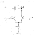
- FIG.1 shows a known laser driver circuit 100, essentially having a differential pair configuration.
- a resistor 104 is coupled to a positive supply voltage rail 102. Also coupled to the supply voltage rail 102 is a laser diode 106.
- the resistor 104 is connected in series with a collector electrode of a first transistor 108.
- An emitter electrode of the first transistor 108 is coupled to a current source 112.
- an emitter electrode of a second transistor 110 is coupled to the current source 112.
- a first signal input lead 116 is coupled to a base electrode of the first transistor 108 and a second signal input lead 118 is coupled to a base electrode of the second transistor 110.
- a high frequency input data signal is applied to the second signal input lead 118 and an inverse input data signal is applied to the first signal input lead 116.
- the first transistor 108 and the second transistor 110 are matched.
- the resistor 104 functions as a means of power dissipation and approximate load matching.
- an impedance mismatch occurs because the sources of the laser driver circuit 100 are first transistor 108 and second transistor 110 of approximate resistance 1k ⁇ , whereas the loads of the circuit are laser diode 106 having equivalent AC resistance of approximately 5 ⁇ and resistor 104 having resistance of typically 30 ⁇ .
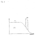
- FIG.2 An example frequency response curve for the laser driver circuit 100 of FIG.1 is illustrated in FIG.2. At relatively lower frequencies the output response 200 maintains a constant value 202 with respect to the input frequency. At high frequencies, resonances 204 are evident which would have a substantial effect on an output signal.
- FIG.3 A circuit diagram comprising a feedback is illustrated in FIG.3.
- the structure of the circuit diagram 300 is the same as that of the circuit diagram shown in FIG.1, with identical features to those of FIG.1 having the same reference numerals as those of FIG.1, but with the prefix "3" instead of the prefix "1".
- resistor 104 in FIG.1 is resistor 304 in FIG.3.
- a feedback impedance 320 is coupled between the collector electrode of the second transistor 310 and the second signal input lead 318.
- the feedback impedance 320 generally comprises a resistor and a capacitor.
- the addition of the feedback impedance 320 acts to feed back the reflected signals from the laser diode 306 and transistor 310 into the second signal input lead 318.
- the magnitude of the resistor and the capacitor within feedback impedance 320 affect the frequency response of the circuit.
- the feedback impedance 320 can mitigate the resonances.
- an optional feedback impedance 322 (indicated by a dotted line in FIG.3) is coupled between the collector electrode of the first transistor 308 and the first signal input lead 316.
- the optional feedback impedance 322 generally comprising a resistor and a capacitor, assists in maintaining the laser driver circuit 300 in a balanced state.
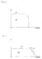
- FIG.4 An example frequency response curve of the laser driver circuit 300 of FIG.3 is illustrated in FIG.4 and in FIG.5.
- the frequency response curve 400 of FIG. 4 results when the resistor and the capacitor of the feedback impedance 320 have relatively low values (for example 600 ⁇ and 5pF, respectively).
- the resistor and capacitor serve to provide a low pass filter with a cut-off frequency determined to be just lower than the resonance frequency.
- the output 400 maintains a constant value 402.
- the output 400 is however cut-off before the very high frequency range (and associated resonances) are reached. Thus, although the bandwidth is reduced, the output power is maintained at lower frequencies.
- the frequency response curve 500 of FIG. 5 results when the resistor and the capacitor of the feedback impedance 320 have relatively high values (for example 2k ⁇ and 20pF, respectively). Again, at lower frequencies the output 500 maintains a constant value 502. However, the output power is somewhat reduced at lower frequencies due to the effect of the feedback impedance. This filtering effect also causes the resonances to be substantially reduced, as shown at resonance peaks 504.
- the feedback impedance would have a very high value capacitor and a low value resistor to provide essentially DC blocking with a flat frequency response.
- the realisation of a very high value capacitor within an integrated circuit causes manufacturing difficulties.
- FIG.6 A circuit diagram according to the present invention is illustrated in FIG.6.
- the structure of the circuit diagram 600 is the same as that of the circuit diagram shown in FIG.1, with identical features to those of FIG.1 having the same reference numerals as those of FIG.1, but with the prefix "6" instead of the prefix "1".
- resistor 104 in FIG.1 is resistor 604 in FIG.6.
- a differential amplifier 620 is coupled between the collector electrode of the second transistor 610 and the base electrode of both the first transistor 608 and the second transistor 610.
- the addition of the differential amplifier 620 acts to feed back the output driving signal from transistor 610 into the first and second signal input leads 616, 618, and has a similar effect to the feedback impedance 320 in FIG.3.
- the present invention provides a system which minimises or removes resonances in a driver circuit
- the invention is simple to implement and relatively cheap to realise.
- the present invention is generally applicable to differential amplifiers and is particularly applicable to laser driver devices.
Landscapes
- Physics & Mathematics (AREA)
- Condensed Matter Physics & Semiconductors (AREA)
- General Physics & Mathematics (AREA)
- Electromagnetism (AREA)
- Optics & Photonics (AREA)
- Semiconductor Lasers (AREA)
Claims (2)
- Eine Treiberschaltung (600) umfasst einen ersten Transistor (610), der eine erste Stromelektrode, die mit einer Stromquelle (612) gekoppelt ist, eine zweite Stromelektrode und eine Steuerelektrode, die mit einem ersten Eingangsanschluss gekoppelt ist, eine Niedrigimpedanzlast (606), die einen ersten Anschluss, der mit der zweiten Stromelektrode des ersten Transistors (610) gekoppelt ist, und einen zweiten Anschluss aufweist, der mit einer Versorgungs-Rail (602) gekoppelt ist, und ein Impedanzelement (602) aufweist, das mit der Steuerelektrode des ersten Transistors (610) gekoppelt ist, um Wechselsignalrückkopplung an denselben zu liefern, wobei der erste Transistor (610) Teil eines Differenzpaars bildet, bei dem ein zweiter Transistor (608) eine erste Stromelektrode, die mit der Stromquelle (612) gekoppelt ist, eine zweite Stromelektrode, die mit einem Widerstandselement (604) gekoppelt ist, und eine Steuerelektrode aufweist, die mit einem zweiten Eingangsanschluss gekoppelt ist, wobei der erste und der zweite Eingangsanschluss Differenzeingänge zum Empfangen von Differenzdatensignalen sind, dadurch gekennzeichnet, dass:das Impedanzelement einen Differenzverstärker (620) umfasst, der einen Eingang, der mit der zweiten Stromelektrode des ersten Transistors gekoppelt ist, und einen ersten und einen zweiten Differenzausgang aufweist, wobei der erste Differenzausgang mit der Steuerelektrode des ersten Transistors (610) gekoppelt ist und der zweite Differenzausgang mit der Steuerelektrode des zweiten Transistors (608) gekoppelt ist.
- Eine Treiberschaltung gemäß Anspruch 1, bei der die Niedrigimpedanzlast (606) eine Laserdiode ist.
Priority Applications (3)
| Application Number | Priority Date | Filing Date | Title |
|---|---|---|---|
| DE60119907T DE60119907T2 (de) | 2001-06-08 | 2001-06-08 | Treiberschaltung |
| EP01305015A EP1265357B1 (de) | 2001-06-08 | 2001-06-08 | Treiberschaltung |
| US10/164,556 US6850546B2 (en) | 2001-06-08 | 2002-06-10 | Driver circuit |
Applications Claiming Priority (1)
| Application Number | Priority Date | Filing Date | Title |
|---|---|---|---|
| EP01305015A EP1265357B1 (de) | 2001-06-08 | 2001-06-08 | Treiberschaltung |
Publications (2)
| Publication Number | Publication Date |
|---|---|
| EP1265357A1 EP1265357A1 (de) | 2002-12-11 |
| EP1265357B1 true EP1265357B1 (de) | 2006-05-24 |
Family
ID=8182016
Family Applications (1)
| Application Number | Title | Priority Date | Filing Date |
|---|---|---|---|
| EP01305015A Expired - Lifetime EP1265357B1 (de) | 2001-06-08 | 2001-06-08 | Treiberschaltung |
Country Status (3)
| Country | Link |
|---|---|
| US (1) | US6850546B2 (de) |
| EP (1) | EP1265357B1 (de) |
| DE (1) | DE60119907T2 (de) |
Families Citing this family (3)
| Publication number | Priority date | Publication date | Assignee | Title |
|---|---|---|---|---|
| US6738401B2 (en) * | 2001-10-11 | 2004-05-18 | Quantum Bridge Communications, Inc. | High speed switching driver |
| US7006543B2 (en) * | 2002-08-30 | 2006-02-28 | Primarion, Inc. | System and circuit for a multi-channel optoelectronic device driver |
| DE602009000366D1 (de) * | 2008-04-25 | 2010-12-30 | Jds Uniphase Corp | Gleichstromgekoppelter Antrieb mit aktiver Terminierung |
Family Cites Families (22)
| Publication number | Priority date | Publication date | Assignee | Title |
|---|---|---|---|---|
| DE2743099A1 (de) * | 1977-09-24 | 1979-04-05 | List Hans | Schaltungsanordnung mit transistoren |
| US4282495A (en) * | 1979-05-29 | 1981-08-04 | The Singer Company | High efficiency current regulator for ring laser gyroscope |
| JP2725307B2 (ja) * | 1988-09-27 | 1998-03-11 | 日本電気株式会社 | トランジスタ増幅器 |
| US5347388A (en) * | 1989-12-01 | 1994-09-13 | Scientific-Atlanta, Inc. | Push-pull optical receiver having gain control |
| US5224111A (en) * | 1991-07-15 | 1993-06-29 | International Business Machines Corporation | Dual fiber drive system |
| JPH07314775A (ja) * | 1994-05-24 | 1995-12-05 | Canon Inc | 発光光量の調整装置及びその方法 |
| JPH08204270A (ja) * | 1995-01-20 | 1996-08-09 | Brother Ind Ltd | 半導体レーザ駆動回路 |
| JP2735042B2 (ja) * | 1995-07-28 | 1998-04-02 | 日本電気株式会社 | 電圧制御型レーザダイオード駆動回路 |
| GB2312346B (en) * | 1996-04-20 | 2000-07-12 | Northern Telecom Ltd | Marshalling in optical tdma systems |
| JP3577392B2 (ja) * | 1996-07-25 | 2004-10-13 | アルプス電気株式会社 | 波形整形回路 |
| JP3545142B2 (ja) * | 1996-11-25 | 2004-07-21 | 三菱電機株式会社 | 差動増幅器 |
| US5883910A (en) * | 1997-07-03 | 1999-03-16 | Maxim Integrated Products, Inc. | High speed semiconductor laser driver circuits |
| JPH11208017A (ja) * | 1998-01-30 | 1999-08-03 | Canon Inc | 発光素子駆動装置 |
| US5974064A (en) * | 1998-04-14 | 1999-10-26 | Optobahn Corporation | Temperature compensation of laser diodes |
| US6021143A (en) * | 1998-04-21 | 2000-02-01 | Lucent Technologies, Inc. | Dynamic control for laser diode drivers |
| US6069523A (en) * | 1998-06-04 | 2000-05-30 | Nortel Networks Corporation | Differential data driver |
| US6285692B1 (en) * | 1998-08-05 | 2001-09-04 | Advantest Corporation | Method and apparatus for driving laser diode |
| US6021144A (en) * | 1999-02-24 | 2000-02-01 | Nvision, Inc. | Automatic power control circuit for a laser driver |
| JP2002542702A (ja) * | 1999-04-16 | 2002-12-10 | コーニンクレッカ フィリップス エレクトロニクス エヌ ヴィ | 増幅器回路 |
| US7555263B1 (en) * | 1999-10-21 | 2009-06-30 | Broadcom Corporation | Adaptive radio transceiver |
| US6441689B1 (en) * | 2001-01-11 | 2002-08-27 | Nokia Networks Oy | Transistor amplifier providing improved linear and return loss performance characteristics |
| EP1267487A1 (de) * | 2001-06-15 | 2002-12-18 | Contraves Space AG | Hochfrequenzverstärker |
-
2001
- 2001-06-08 EP EP01305015A patent/EP1265357B1/de not_active Expired - Lifetime
- 2001-06-08 DE DE60119907T patent/DE60119907T2/de not_active Expired - Lifetime
-
2002
- 2002-06-10 US US10/164,556 patent/US6850546B2/en not_active Expired - Fee Related
Also Published As
| Publication number | Publication date |
|---|---|
| US6850546B2 (en) | 2005-02-01 |
| DE60119907T2 (de) | 2006-09-28 |
| DE60119907D1 (de) | 2006-06-29 |
| US20020186733A1 (en) | 2002-12-12 |
| EP1265357A1 (de) | 2002-12-11 |
Similar Documents
| Publication | Publication Date | Title |
|---|---|---|
| EP1276230B1 (de) | Kaskodenkettenverstärker | |
| EP0664937B1 (de) | Leitungstreiber mit adaptiver ausgangsimpedanz | |
| EP0426594A2 (de) | Temperaturkompensierter Rückkopplungskreis zum Einstellen und Stabilisieren von Verstärkerarbeitspunkten | |
| EP0702436B1 (de) | Lasermodul mit Impedanzanpassungstransformator | |
| EP1289081A1 (de) | Lasertreiberschaltung und Verfahren zum Treiben eines Lasers | |
| EP2112727A1 (de) | Gleichstromgekoppelter Antrieb mit aktiver Terminierung | |
| US4004253A (en) | Variable equalizer | |
| JPH09214278A (ja) | Pinダイオード可変減衰器 | |
| US2760007A (en) | Two-stage transistor feedback amplifier | |
| US11329729B2 (en) | Optical receiver circuit, optical receiver, optical terminal device, and optical communication system | |
| US7075381B2 (en) | Oscillator circuit and oscillator | |
| EP0788680B1 (de) | Elektronischer lampenballast der eine brückenschaltung enthält und integrierte schaltung mit spannungs-stromkonverter zur steuerung der brückenschaltung | |
| US7170346B2 (en) | Arrangement for reducing non-linear distortions in an output signal of an amplifier stage | |
| US6850546B2 (en) | Driver circuit | |
| EP0732807B1 (de) | Steuerbare Filteranordnung | |
| EP1434348A1 (de) | Breitband-Gleichtaktregler | |
| EP1261124B1 (de) | Eine Verstärkerstufe mit variabler Verstärkung | |
| US5834988A (en) | Frequency compensated PIN diode attenuator | |
| EP0583398A1 (de) | Treiberverstärker für netzleitungsübertragung | |
| JPH11234063A (ja) | 高周波用増幅器 | |
| JP2003032050A (ja) | プリアンプ回路 | |
| AU703005B2 (en) | Circuit arrangement of an ultra-broadband receiver | |
| US6414544B2 (en) | Demodulation filter | |
| JPH06284090A (ja) | 光受信器 | |
| JP2005252783A (ja) | 光送信機 |
Legal Events
| Date | Code | Title | Description |
|---|---|---|---|
| PUAI | Public reference made under article 153(3) epc to a published international application that has entered the european phase |
Free format text: ORIGINAL CODE: 0009012 |
|
| AK | Designated contracting states |
Kind code of ref document: A1 Designated state(s): AT BE CH CY DE DK ES FI FR GB GR IE IT LI LU MC NL PT SE TR |
|
| AX | Request for extension of the european patent |
Free format text: AL;LT;LV;MK;RO;SI |
|
| 17P | Request for examination filed |
Effective date: 20030611 |
|
| AKX | Designation fees paid |
Designated state(s): DE GB |
|
| 17Q | First examination report despatched |
Effective date: 20050704 |
|
| GRAP | Despatch of communication of intention to grant a patent |
Free format text: ORIGINAL CODE: EPIDOSNIGR1 |
|
| GRAS | Grant fee paid |
Free format text: ORIGINAL CODE: EPIDOSNIGR3 |
|
| GRAA | (expected) grant |
Free format text: ORIGINAL CODE: 0009210 |
|
| AK | Designated contracting states |
Kind code of ref document: B1 Designated state(s): DE GB |
|
| REG | Reference to a national code |
Ref country code: GB Ref legal event code: FG4D |
|
| REF | Corresponds to: |
Ref document number: 60119907 Country of ref document: DE Date of ref document: 20060629 Kind code of ref document: P |
|
| REG | Reference to a national code |
Ref country code: GB Ref legal event code: 732E |
|
| PGFP | Annual fee paid to national office [announced via postgrant information from national office to epo] |
Ref country code: GB Payment date: 20060825 Year of fee payment: 6 |
|
| RAP2 | Party data changed (patent owner data changed or rights of a patent transferred) |
Owner name: AVAGO TECHNOLOGIES FIBER IP (SINGAPORE) PTE. LTD. |
|
| PLBE | No opposition filed within time limit |
Free format text: ORIGINAL CODE: 0009261 |
|
| STAA | Information on the status of an ep patent application or granted ep patent |
Free format text: STATUS: NO OPPOSITION FILED WITHIN TIME LIMIT |
|
| 26N | No opposition filed |
Effective date: 20070227 |
|
| GBPC | Gb: european patent ceased through non-payment of renewal fee |
Effective date: 20070608 |
|
| PG25 | Lapsed in a contracting state [announced via postgrant information from national office to epo] |
Ref country code: GB Free format text: LAPSE BECAUSE OF NON-PAYMENT OF DUE FEES Effective date: 20070608 |
|
| PGFP | Annual fee paid to national office [announced via postgrant information from national office to epo] |
Ref country code: DE Payment date: 20100602 Year of fee payment: 10 |
|
| REG | Reference to a national code |
Ref country code: DE Ref legal event code: R119 Ref document number: 60119907 Country of ref document: DE Effective date: 20120103 |
|
| PG25 | Lapsed in a contracting state [announced via postgrant information from national office to epo] |
Ref country code: DE Free format text: LAPSE BECAUSE OF NON-PAYMENT OF DUE FEES Effective date: 20120103 |