EP1270233B1 - Geschlitzes Substrat und Verfahren zum Schneiden - Google Patents
Geschlitzes Substrat und Verfahren zum Schneiden Download PDFInfo
- Publication number
- EP1270233B1 EP1270233B1 EP02254048A EP02254048A EP1270233B1 EP 1270233 B1 EP1270233 B1 EP 1270233B1 EP 02254048 A EP02254048 A EP 02254048A EP 02254048 A EP02254048 A EP 02254048A EP 1270233 B1 EP1270233 B1 EP 1270233B1
- Authority
- EP
- European Patent Office
- Prior art keywords
- substrate
- layer
- slot
- plug
- etching
- Prior art date
- Legal status (The legal status is an assumption and is not a legal conclusion. Google has not performed a legal analysis and makes no representation as to the accuracy of the status listed.)
- Expired - Lifetime
Links
- 239000000758 substrate Substances 0.000 title claims description 119
- 238000000034 method Methods 0.000 title claims description 24
- 230000000873 masking effect Effects 0.000 claims description 25
- 238000005530 etching Methods 0.000 claims description 19
- 238000010304 firing Methods 0.000 claims description 17
- 239000012530 fluid Substances 0.000 claims description 16
- WGTYBPLFGIVFAS-UHFFFAOYSA-M tetramethylammonium hydroxide Chemical compound [OH-].C[N+](C)(C)C WGTYBPLFGIVFAS-UHFFFAOYSA-M 0.000 claims description 14
- 238000000151 deposition Methods 0.000 claims description 7
- 238000000059 patterning Methods 0.000 claims description 6
- 238000004519 manufacturing process Methods 0.000 claims description 4
- 230000004888 barrier function Effects 0.000 description 19
- 239000000463 material Substances 0.000 description 16
- 235000012431 wafers Nutrition 0.000 description 15
- VYPSYNLAJGMNEJ-UHFFFAOYSA-N Silicium dioxide Chemical compound O=[Si]=O VYPSYNLAJGMNEJ-UHFFFAOYSA-N 0.000 description 10
- XUIMIQQOPSSXEZ-UHFFFAOYSA-N Silicon Chemical compound [Si] XUIMIQQOPSSXEZ-UHFFFAOYSA-N 0.000 description 9
- 229910052710 silicon Inorganic materials 0.000 description 9
- 239000010703 silicon Substances 0.000 description 9
- 238000002161 passivation Methods 0.000 description 8
- 239000010409 thin film Substances 0.000 description 7
- 238000000623 plasma-assisted chemical vapour deposition Methods 0.000 description 6
- 238000004544 sputter deposition Methods 0.000 description 6
- 229910052581 Si3N4 Inorganic materials 0.000 description 5
- 239000000377 silicon dioxide Substances 0.000 description 5
- 235000012239 silicon dioxide Nutrition 0.000 description 5
- 229910052715 tantalum Inorganic materials 0.000 description 5
- GUVRBAGPIYLISA-UHFFFAOYSA-N tantalum atom Chemical group [Ta] GUVRBAGPIYLISA-UHFFFAOYSA-N 0.000 description 5
- BOTDANWDWHJENH-UHFFFAOYSA-N Tetraethyl orthosilicate Chemical compound CCO[Si](OCC)(OCC)OCC BOTDANWDWHJENH-UHFFFAOYSA-N 0.000 description 4
- 229910052782 aluminium Inorganic materials 0.000 description 4
- XAGFODPZIPBFFR-UHFFFAOYSA-N aluminium Chemical compound [Al] XAGFODPZIPBFFR-UHFFFAOYSA-N 0.000 description 4
- 239000002131 composite material Substances 0.000 description 4
- 238000001704 evaporation Methods 0.000 description 4
- 230000008020 evaporation Effects 0.000 description 4
- 239000011521 glass Substances 0.000 description 4
- HBMJWWWQQXIZIP-UHFFFAOYSA-N silicon carbide Chemical compound [Si+]#[C-] HBMJWWWQQXIZIP-UHFFFAOYSA-N 0.000 description 4
- 229910010271 silicon carbide Inorganic materials 0.000 description 4
- HQVNEWCFYHHQES-UHFFFAOYSA-N silicon nitride Chemical compound N12[Si]34N5[Si]62N3[Si]51N64 HQVNEWCFYHHQES-UHFFFAOYSA-N 0.000 description 4
- 239000004020 conductor Substances 0.000 description 3
- 230000008878 coupling Effects 0.000 description 3
- 238000010168 coupling process Methods 0.000 description 3
- 238000005859 coupling reaction Methods 0.000 description 3
- 230000000694 effects Effects 0.000 description 3
- 229920000642 polymer Polymers 0.000 description 3
- IJGRMHOSHXDMSA-UHFFFAOYSA-N Atomic nitrogen Chemical compound N#N IJGRMHOSHXDMSA-UHFFFAOYSA-N 0.000 description 2
- RYGMFSIKBFXOCR-UHFFFAOYSA-N Copper Chemical compound [Cu] RYGMFSIKBFXOCR-UHFFFAOYSA-N 0.000 description 2
- KRHYYFGTRYWZRS-UHFFFAOYSA-N Fluorane Chemical compound F KRHYYFGTRYWZRS-UHFFFAOYSA-N 0.000 description 2
- KWYUFKZDYYNOTN-UHFFFAOYSA-M Potassium hydroxide Chemical compound [OH-].[K+] KWYUFKZDYYNOTN-UHFFFAOYSA-M 0.000 description 2
- RVSGESPTHDDNTH-UHFFFAOYSA-N alumane;tantalum Chemical compound [AlH3].[Ta] RVSGESPTHDDNTH-UHFFFAOYSA-N 0.000 description 2
- 239000011153 ceramic matrix composite Substances 0.000 description 2
- 229910052802 copper Inorganic materials 0.000 description 2
- 239000010949 copper Substances 0.000 description 2
- 230000008021 deposition Effects 0.000 description 2
- 239000003989 dielectric material Substances 0.000 description 2
- 239000010408 film Substances 0.000 description 2
- 239000011156 metal matrix composite Substances 0.000 description 2
- 239000000203 mixture Substances 0.000 description 2
- TWNQGVIAIRXVLR-UHFFFAOYSA-N oxo(oxoalumanyloxy)alumane Chemical compound O=[Al]O[Al]=O TWNQGVIAIRXVLR-UHFFFAOYSA-N 0.000 description 2
- DDFHBQSCUXNBSA-UHFFFAOYSA-N 5-(5-carboxythiophen-2-yl)thiophene-2-carboxylic acid Chemical compound S1C(C(=O)O)=CC=C1C1=CC=C(C(O)=O)S1 DDFHBQSCUXNBSA-UHFFFAOYSA-N 0.000 description 1
- OKTJSMMVPCPJKN-UHFFFAOYSA-N Carbon Chemical compound [C] OKTJSMMVPCPJKN-UHFFFAOYSA-N 0.000 description 1
- 239000004593 Epoxy Substances 0.000 description 1
- 229910018487 Ni—Cr Inorganic materials 0.000 description 1
- BLRPTPMANUNPDV-UHFFFAOYSA-N Silane Chemical compound [SiH4] BLRPTPMANUNPDV-UHFFFAOYSA-N 0.000 description 1
- NRTOMJZYCJJWKI-UHFFFAOYSA-N Titanium nitride Chemical compound [Ti]#N NRTOMJZYCJJWKI-UHFFFAOYSA-N 0.000 description 1
- QVGXLLKOCUKJST-UHFFFAOYSA-N atomic oxygen Chemical compound [O] QVGXLLKOCUKJST-UHFFFAOYSA-N 0.000 description 1
- 230000015572 biosynthetic process Effects 0.000 description 1
- 229910052799 carbon Inorganic materials 0.000 description 1
- BGTFCAQCKWKTRL-YDEUACAXSA-N chembl1095986 Chemical compound C1[C@@H](N)[C@@H](O)[C@H](C)O[C@H]1O[C@@H]([C@H]1C(N[C@H](C2=CC(O)=CC(O[C@@H]3[C@H]([C@@H](O)[C@H](O)[C@@H](CO)O3)O)=C2C=2C(O)=CC=C(C=2)[C@@H](NC(=O)[C@@H]2NC(=O)[C@@H]3C=4C=C(C(=C(O)C=4)C)OC=4C(O)=CC=C(C=4)[C@@H](N)C(=O)N[C@@H](C(=O)N3)[C@H](O)C=3C=CC(O4)=CC=3)C(=O)N1)C(O)=O)=O)C(C=C1)=CC=C1OC1=C(O[C@@H]3[C@H]([C@H](O)[C@@H](O)[C@H](CO[C@@H]5[C@H]([C@@H](O)[C@H](O)[C@@H](C)O5)O)O3)O[C@@H]3[C@H]([C@@H](O)[C@H](O)[C@@H](CO)O3)O[C@@H]3[C@H]([C@H](O)[C@@H](CO)O3)O)C4=CC2=C1 BGTFCAQCKWKTRL-YDEUACAXSA-N 0.000 description 1
- VNNRSPGTAMTISX-UHFFFAOYSA-N chromium nickel Chemical compound [Cr].[Ni] VNNRSPGTAMTISX-UHFFFAOYSA-N 0.000 description 1
- 230000007797 corrosion Effects 0.000 description 1
- 238000005260 corrosion Methods 0.000 description 1
- 238000004132 cross linking Methods 0.000 description 1
- 239000013078 crystal Substances 0.000 description 1
- 230000007547 defect Effects 0.000 description 1
- -1 field oxide Chemical compound 0.000 description 1
- 239000000945 filler Substances 0.000 description 1
- PCHJSUWPFVWCPO-UHFFFAOYSA-N gold Chemical compound [Au] PCHJSUWPFVWCPO-UHFFFAOYSA-N 0.000 description 1
- 229910052737 gold Inorganic materials 0.000 description 1
- 239000010931 gold Substances 0.000 description 1
- 238000010438 heat treatment Methods 0.000 description 1
- 239000012535 impurity Substances 0.000 description 1
- 239000004615 ingredient Substances 0.000 description 1
- 239000011159 matrix material Substances 0.000 description 1
- 229910052751 metal Inorganic materials 0.000 description 1
- 239000002184 metal Substances 0.000 description 1
- 229910021421 monocrystalline silicon Inorganic materials 0.000 description 1
- 238000009740 moulding (composite fabrication) Methods 0.000 description 1
- 229910052757 nitrogen Inorganic materials 0.000 description 1
- 229920000620 organic polymer Polymers 0.000 description 1
- 229910052760 oxygen Inorganic materials 0.000 description 1
- 239000001301 oxygen Substances 0.000 description 1
- 239000002245 particle Substances 0.000 description 1
- 239000011160 polymer matrix composite Substances 0.000 description 1
- 229920001296 polysiloxane Polymers 0.000 description 1
- 239000004065 semiconductor Substances 0.000 description 1
- 229910000077 silane Inorganic materials 0.000 description 1
- WNUPENMBHHEARK-UHFFFAOYSA-N silicon tungsten Chemical compound [Si].[W] WNUPENMBHHEARK-UHFFFAOYSA-N 0.000 description 1
- 239000000126 substance Substances 0.000 description 1
- 238000003631 wet chemical etching Methods 0.000 description 1
Images

Classifications
-
- B—PERFORMING OPERATIONS; TRANSPORTING
- B41—PRINTING; LINING MACHINES; TYPEWRITERS; STAMPS
- B41J—TYPEWRITERS; SELECTIVE PRINTING MECHANISMS, i.e. MECHANISMS PRINTING OTHERWISE THAN FROM A FORME; CORRECTION OF TYPOGRAPHICAL ERRORS
- B41J2/00—Typewriters or selective printing mechanisms characterised by the printing or marking process for which they are designed
- B41J2/005—Typewriters or selective printing mechanisms characterised by the printing or marking process for which they are designed characterised by bringing liquid or particles selectively into contact with a printing material
- B41J2/01—Ink jet
- B41J2/135—Nozzles
- B41J2/16—Production of nozzles
- B41J2/1601—Production of bubble jet print heads
- B41J2/1603—Production of bubble jet print heads of the front shooter type
-
- B—PERFORMING OPERATIONS; TRANSPORTING
- B41—PRINTING; LINING MACHINES; TYPEWRITERS; STAMPS
- B41J—TYPEWRITERS; SELECTIVE PRINTING MECHANISMS, i.e. MECHANISMS PRINTING OTHERWISE THAN FROM A FORME; CORRECTION OF TYPOGRAPHICAL ERRORS
- B41J2/00—Typewriters or selective printing mechanisms characterised by the printing or marking process for which they are designed
- B41J2/005—Typewriters or selective printing mechanisms characterised by the printing or marking process for which they are designed characterised by bringing liquid or particles selectively into contact with a printing material
- B41J2/01—Ink jet
- B41J2/135—Nozzles
- B41J2/16—Production of nozzles
- B41J2/1621—Manufacturing processes
- B41J2/1626—Manufacturing processes etching
- B41J2/1629—Manufacturing processes etching wet etching
-
- B—PERFORMING OPERATIONS; TRANSPORTING
- B41—PRINTING; LINING MACHINES; TYPEWRITERS; STAMPS
- B41J—TYPEWRITERS; SELECTIVE PRINTING MECHANISMS, i.e. MECHANISMS PRINTING OTHERWISE THAN FROM A FORME; CORRECTION OF TYPOGRAPHICAL ERRORS
- B41J2/00—Typewriters or selective printing mechanisms characterised by the printing or marking process for which they are designed
- B41J2/005—Typewriters or selective printing mechanisms characterised by the printing or marking process for which they are designed characterised by bringing liquid or particles selectively into contact with a printing material
- B41J2/01—Ink jet
- B41J2/135—Nozzles
- B41J2/16—Production of nozzles
- B41J2/1621—Manufacturing processes
- B41J2/1631—Manufacturing processes photolithography
-
- B—PERFORMING OPERATIONS; TRANSPORTING
- B41—PRINTING; LINING MACHINES; TYPEWRITERS; STAMPS
- B41J—TYPEWRITERS; SELECTIVE PRINTING MECHANISMS, i.e. MECHANISMS PRINTING OTHERWISE THAN FROM A FORME; CORRECTION OF TYPOGRAPHICAL ERRORS
- B41J2/00—Typewriters or selective printing mechanisms characterised by the printing or marking process for which they are designed
- B41J2/005—Typewriters or selective printing mechanisms characterised by the printing or marking process for which they are designed characterised by bringing liquid or particles selectively into contact with a printing material
- B41J2/01—Ink jet
- B41J2/135—Nozzles
- B41J2/16—Production of nozzles
- B41J2/1621—Manufacturing processes
- B41J2/164—Manufacturing processes thin film formation
- B41J2/1642—Manufacturing processes thin film formation thin film formation by CVD [chemical vapor deposition]
Definitions
- the present invention relates to slotted substrates, used in microfluidic devices such as fluid ejection devices.
- thermally actuated printheads use resistive or heating elements to achieve fluid or ink expulsion.
- a representative thermal inkjet printhead has a plurality of thin film resistors provided on a semiconductor substrate.
- a top layer defines firing chambers about each of the resistors. Propagation of a current or a "fire signal" through the resistor causes ink in a corresponding firing chamber to be heated and expelled through a corresponding nozzle.
- fluid is routed to the firing chamber through a slot in the substrate.
- the slot is formed while the substrate is part of a wafer die.
- slots are formed in the wafer die by wet chemical etching of the substrate with, for example, Tetra Methyl Ammonium Hydroxide (TMAH) or potassium hydroxide (KOH).
- TMAH Tetra Methyl Ammonium Hydroxide
- KOH potassium hydroxide
- the etch rate for alkaline chemistries is different for different crystalline planes, and therefore the etch geometry is defined by the orientation of the crystalline planes.
- TMAH etching techniques result in etch angles that cause a very wide backside slot opening. The wide backside opening limits how close the slots can be placed to each other on the die.
- the substrate is often coated with masking films or layers that are substantially unaffected by the etchants.
- these films or layers are typically undercut as a result of extended etching time. Because of this, the etching time is often carefully monitored.
- a method of manufacturing a slotted substrate includes forming a masking layer over a first surface of a substrate, and patterning and etching the masking layer to form a hole therethrough.
- the first layer is deposited over the masking layer and in the hole.
- the first layer is patterned and etched to form a plug in the hole.
- a second surface of the substrate that is opposite the first surface is continuously etched until a bottom surface of the plug is substantially exposed and a slot in the substrate is substantially formed.
- Fig. 1 is a perspective view of an inkjet cartridge 10 with a printhead 14 of an embodiment of the present invention.
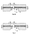
- Fig. 2A illustrates a partial bottom view of the printhead through section 2A-2A of Fig. 1.
- Fig. 2B illustrates a cross-sectional view of the printhead where a thin film stack is applied over a substrate 102.
- a slot region 126 having sloped trench walls 128 is defined in the substrate 102.
- the slot 126 is etched with dimensional control within 1 micron using the present invention.
- using this embodiment enables a higher density of slots to be etched in a given die.
- a capping layer 104 As shown in the embodiment of Figs. 2A and 2B, formed or deposited upon the substrate 102 are at least the following layers: a capping layer 104, a resistive layer 107, a conductive layer 108, a passivation layer 110, a cavitation barrier layer 111, and a barrier layer 112.
- the thin film stack is patterned and etched to form resistors of the resistive layer, conductive traces of the conductive layer, and a firing chamber 130 in the barrier layer.
- the barrier layer 112 defines the firing chamber 130, and a nozzle orifice 132 associated with the firing chamber through which the fluid is ejected.
- Propagation of a current or a "fire signal" through a resistor causes the fluid in the firing chamber 130 to be heated and expelled through the nozzle orifice 132.
- an orifice layer (not shown) having the orifices 132 is applied over the barrier layer 112.
- the sloped trench walls 128 of the slot 126 are formed under the rows of firing chambers and their corresponding resistors and orifices of the printhead.
- the capping layer 104 couples the trench walls 128 at a narrower slot section, as shown in Fig. 2A.
- a channel 129 is formed as a hole or fluid feed slot through the capping layer 104, and the rest of the thin film stack.
- the channel 129 fluidically couples the firing chamber 130 and the slot 126, such that fluid flows through the slot 126 and into the firing chamber 130 via channel 129.
- entrances to the channels 129 are substantially rectangular and substantially parallel to each other along the capping layer 104, as shown in Fig. 2A.
- each channel 129 leads from the slotted substrate to the corresponding firing chamber 130 through the thin film stack.
- the channels 129 fluidically couple the slotted substrate with a single firing chamber 130.
- the channels 129 are used as a filter, such that if a particle is caught in one of the channels 129, the firing chamber 130 operates with fluid supplied through another of the channels 129 that is fluidically coupled with that firing chamber.
- the slot 126 is formed after the thin film stack is deposited on the front side of the substrate. After the thin films layers 104, 107, 108, 110, 111 are formed, a front side protection (or plug) layer 106 is deposited in the channel 129. The layer 112 is then formed thereover. Then the slot 126 is etched, as shown in Fig. 3. After the slot is formed, the layer 106 is removed from the channel 129 with a BOE (buffered oxide etch), as described in more detail below. In one particular embodiment, no additional etching of the slot is performed after the plug is removed.
- BOE biuffered oxide etch
- At least one layer is formed on the substrate 102 when the substrate is etched and the slot 126 is formed.
- the at least one layer formed on the substrate is shown as the capping layer 104.
- the layer 104 masks the substrate 102 to prevent inadvertent etching of the substrate.
- the present invention is not so limited to the one layer 104.
- Embodiments of the present invention include having any number and type of layers deposited over the substrate, depending upon the application for which the slotted substrate is to be utilized. Examples of such additional layers are described herein. In another embodiment, additional layers are deposited over the substrate after the slot is formed (and the front side protection 106 is removed).
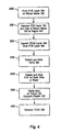
- the slotted substrate is formed as illustrated in Figs. 5 to 11.
- a first capping layer 104 is deposited or grown over a top surface of the substrate 102.
- the capping layer 104 is FOX (field oxide) and the substrate 102 is a silicon wafer.
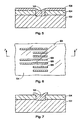
- the FOX layer is patterned and etched to form a hole through the FOX layer 104 and partially into the substrate 102.
- the hole defines a region 122 (See Fig. 5).
- the region 122 is the hole of the capping layer 104, and does not extend past the capping layer 104 into the substrate.
- the front side protection (FSP) layer 106 is deposited over the capping layer 104 and into the region 122.
- the FSP layer 106 is TEOS (tetraethylorthosilicate).
- the method of deposition for TEOS is CVD.
- the FSP layer 106 is at least one of silicon dioxide, silane-based silicon dioxide, silicon nitride, field oxide, silicon carbide, and silicon oxynitride.
- the method of deposition is PECVD.
- a top surface of the FSP layer 106 slopes down towards the substrate 102.
- the FSP layer 106 is patterned and etched to form a plug in the region 122.
- the plug is elongated and extends across the layer 104 substantially following the region 122. In the embodiment shown, edges of the plug extend over the capping layer 104.
- Fig. 6 shows a top view of part of the coated substrate with the plugs of the FSP layer 106 (where the fluid feed channels 29 are to be formed, while Fig. 2A illustrates the fluid feed channels 29 from the bottom).
- the plugs are substantially aligned in at least one of rows and columns. In another embodiment, the plugs are substantially not aligned with other plugs in the substrate.
- a second capping layer 104 is patterned and etched on a bottom surface (or back side) of the substrate, opposite the top surface.
- the etched area of the second capping layer corresponds to and is aligned with the region 122 at the front side of the substrate.
- the etched area of the second capping layer also corresponds to and defines a bottom area of the slot 126 to be etched through the substrate in one embodiment, as described in more detail below.
- the second capping layer 104 is patterned and etched to expose the back side of the substrate opposite the region 122.
- the exposed back side of the substrate has a much larger cross-sectional area than the region 122.
- the second capping (or masking) layer 104 is formed, patterned and etched on the back side of the substrate with the forming, patterning and etching of the capping layer 104 on the front side of the substrate in steps 200 and 210.
- the second capping layer is of the same material as the first capping layer.
- the first and second capping layers are different materials, and the second capping layer is a material that is discussed below as an alternative capping layer material.
- the slot or trench 126 is etched from the back side of the substrate starting at the exposed area (the area not masked by the second capping layer 104).
- the substrate is etched with TMAH (Tetra Methyl Ammonium Hydroxide).
- the substrate is etched with potassium hydroxide (KOH) or another alkaline etchant.
- the substrate is a silicon wafer with ⁇ 100> orientation, such that the wafer is etched at an angle a of about 54.7 degrees with the front and back sides (top and bottom surfaces) of the substrate.
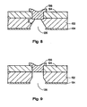
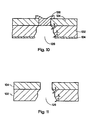
- the slot 126 begins at the exposed area and expands as a substantially pyramidal shape (with walls at an angle a of about 54.7 degrees) until a top of the pyramidal shape reaches the plug of the FSP layer 106, as shown in Fig. 8. Generally, the slot 126 expands in cross-sectional area in the substrate with increasing etch time.
- the wafer is etched to a further step from Fig. 8.
- the slot upon reaching the plug in Fig. 8, the slot then begins to expand along the FSP layer to a substantially truncated pyramidal shape.
- the etch rate along the FSP/substrate interface is greater than the etch rate of the substrate alone and much greater than the FSP layer alone.
- the FSP/substrate interface etch rate is greater than about twice the etch rate of the substrate prior to break through.
- this faster etch along this FSP/substrate interface is called "etch back." Because of this 'etch back,' the substrate is etched along the interface to form slot walls that are not significantly angled (especially when compared with angle a) in a top portion of the substrate, as shown in the process step of Fig. 9. In this embodiment, in the bottom portion of the substrate the sloped walls continue to expand in cross-sectional area during the etch, but remain at an angle a of about 54.7 degrees as they expand. In effect, the wet etched trenches in this embodiment rapidly align to edges of the front side protection structures. In one embodiment, the walls in the bottom portion of the substrate etch at a slower rate than the walls in the upper portion. Additionally in one embodiment, the FSP layer 106 is etched as well, but also at a slower rate than the substrate is etched.
- the wafer is etched to a further step from Fig. 9.
- the walls are sloped with angle a, and in the bottom portion of the slot the walls are also sloped with angle a.
- between the sloped walls of the top and bottom portions are middle walls coupling the substantially truncated pyramidal shapes.
- these coupling middle walls are substantially straight.
- the second capping (or masking) layer 104 substantially stopped the coupling middle walls, as well as the walls in the bottom portion, from expanding to the substantially pyramidal shape, as described in more detail below.
- the substrate begins to etch at the angle ⁇ in the truncated pyramidal shape upon exposure of the capping layer at a capping/substrate interface.
- the slot walls 128 along the bottom portion of the substrate also expand tending towards forming the substantially pyramidal shape throughout the entire slot.
- the walls along the bottom portion of the substrate are substantially unable to expand much beyond edges of the second capping (or masking) layer 104.
- the slow etch rate of the masking layer, and a tendency to maintain the angle ⁇ walls at the bottom portion substantially keeps the slot 126 from expanding beyond the masking layer boundaries.
- the second capping layer 104, the FSP layer 106, and the first capping layer 104 are all etched at a much slower rate than the substrate.
- the etch rate along the capping/substrate interface is greater than the etch rate of the substrate alone and much greater than the capping layer alone.
- the etching is stopped when the shape of the slot reaches that as shown in Fig. 10.
- the substrate is etched for a long enough period and/or the second capping (or masking) layer 104 is masked such that the pyramidal shaped slot is formed.
- the masking layer (or second capping layer) is patterned to keep the first capping layer 104 from being substantially undercut in undesirable areas.
- the channel entrance 129 for the fluid is not in the center of the slot 126 (see for instance, Figs. 2A, 2B, and 6).
- the slotted substrate is formed substantially the same in either instance where the entrance 129 is centrally located or off-center, due to the "etch back" described with regard to Fig. 9.
- the slotted substrate still is substantially formed as shown in Figs. 4 to 11, and described above.
- the plug is utilized to align the trench to the hole etched into region 122 of the masking layer 104 on the front side of the substrate.
- dimensions of the hole (or channel 129 opening) substantially correspond to dimensions of the plug.
- the substrate first quickly etches along the FSP/substrate interface, then along the capping/substrate interface.
- Each of the adjacent (and substantially parallel) FSP/substrate interfaces (see Figs. 2A and 6) etch toward forming the substantially truncated pyramidal shape slotted walls.
- the pyramidal shaped slots from each of the FSP/substrate interfaces overlap. After they overlap, the slots quickly combine and expand to their new boundaries, eventually becoming one large truncated pyramidal shaped slot 126 (see Fig. 2A).
- the capping/substrate interfaces between the FSP/substrate interfaces are also quickly etched.
- the slot walls 128 are not yet aligned, due to the staggering of the regions 122 (see Fig. 6).
- each of the walls 128 of the one large slot have a tendency to eventually substantially align with each other throughout the substrate thereby reaching an equilibrium state of the truncated pyramidal shape. Consequently, the capping/substrate interfaces that surround the regions 122 (or FSP/substrate interfaces of Fig. 2A) etch back to align the slot walls 128 to each other.
- the walls 128 substantially align with each other because the etch rate of the capping/substrate interface is greater than that for the substrate, especially when the slot is striving to reach the equilibrium state.
- the slot through the wafer is substantially formed and the TMAH process substantially complete in 12 hours.
- the slot through the 625 micron wafer is substantially formed in 11 1 ⁇ 2 hours.
- the slot is formed between about 10 1/2 and 12 hours, depending upon the size of the wafer and the size of the slot desired.
- the time for "etch back" for low BDD (bulk defect density) silicon wafers is between about 1 ⁇ 2 and 1 hour.
- the region 122 has a width that ranges from about 40 microns to about 120 microns, depending upon the substrate and processes used. In one embodiment, the region 122 width is about 80 to 110 microns.
- the FSP layer 106 or plug is removed from the region 122.
- TEOS is removed with a buffered oxide etch (BOE).
- BOE is a mix of hydrofluoric acid and ammonium fluoride.
- the etch is aqueous and may be any mixture strength of the two primary ingredients.
- the hydrofluoric solution is diluted.
- the BOE process is substantially completed in about 10 minutes. However, the BOE process may be completed in as little as 5 minutes.
- the substrate 102 is a monocrystalline silicon wafer.
- the substrate wafer is low BDD (low number of imperfections in the silicon crystal lattice).
- the wafer has approximately 525 microns of thickness for a four-inch diameter or approximately 625 microns of thickness for a six-inch diameter.
- the silicon substrate is p-type, lightly doped to approximately 0.55 ohm/cm.
- the starting substrate may be glass, a semiconductive material, a Metal Matrix Composite (MMC), a Ceramic Matrix Composite (CMC), a Polymer Matrix Composite (PMC) or a sandwich Si/xMc, in which the x filler material is etched out of the composite matrix post vacuum processing.
- MMC Metal Matrix Composite
- CMC Ceramic Matrix Composite
- PMC Polymer Matrix Composite
- sandwich Si/xMc sandwich Si/xMc
- the layer 104 covers and seals the substrate 102, thereby providing a barrier layer.
- the capping layer 104 electrically insulates the substrate 102.
- Capping layer 104 may be formed of a variety of different materials such as silicon dioxide, aluminum oxide, silicon carbide, silicon nitride, glass (PSG), and/or an electrically insulating dielectric material.
- the capping layer 104 is a thermal barrier layer.
- the capping layer may be formed using any of a variety of methods known to those skilled in the art such as thermally growing the layer, sputtering, evaporation, and plasma enhanced chemical vapor deposition (PECVD).
- PECVD plasma enhanced chemical vapor deposition
- the thickness of capping layer may be any desired thickness sufficient to cover and seal the substrate. Generally, the capping layer has a thickness of up to about 1 to 2 microns.
- the layer 104 is a phosphorous-doped (n+) silicon dioxide interdielectric, insulating glass layer (PSG) deposited by PECVD techniques.
- PSG phosphorous-doped
- the PSG layer has a thickness of up to about 1 to 2 microns. In one embodiment, this layer is approximately 0.5 micron thick and forms the remainder of the thermal inkjet heater resistor oxide underlayer. In another embodiment, the thickness range is about 0.7 to 0.9 microns.
- the capping layer 104 is field oxide (FOX) that is thermally grown on the exposed substrate 102.
- FOX field oxide
- the process grows the FOX into the silicon substrate as well as depositing it on top to form a total depth of approximately 1.3 microns. Because the FOX layer pulls the silicon from the substrate, a strong chemical bond is established between the FOX layer and the substrate.
- the resistive layer 107 is formed by depositing resistive material over the layer 104.
- sputter deposition techniques are used to deposit a resistive material layer of tantalum aluminum composite.
- the composite has a resistivity of approximately 30 ohms/square.
- the layer forming the resistor has a thickness in the range of about 500 angstroms to 2000 angstroms. However, resistor layers with thicknesses outside this range are also within the scope of the invention.
- resistive materials are known to those skilled in the art including tantalum aluminum, nickel chromium, tungsten silicon nitride, and titanium nitride, which may optionally be doped with suitable impurities such as oxygen, nitrogen, and carbon, to adjust the resistivity of the material.
- the resistive material may be deposited by any suitable method such as sputtering, and evaporation.
- the conductive layer 108 is formed by depositing conductive material over the resistive layer 107.
- the conductive material is formed of at least one of a variety of different materials including aluminum, aluminum with about 1 ⁇ 2 % copper, copper, gold, and aluminum with 1 ⁇ 2% silicon, and may be deposited by any method, such as sputtering and evaporation. Generally, the conductive layer has a thickness of up to about 1 to 2 microns. In one embodiment, sputter deposition is used to deposit a layer of aluminum to a thickness of approximately 0.5 micron.
- the conductive layer 108 and the resistive layer 107 are patterned and etched to form resistors and conductive traces.
- the insulating passivation layer 110 is formed over the resistors and conductor traces to prevent electrical charging of the fluid or corrosion of the device, in the event that an electrically conductive fluid is used.
- Passivation layer 1 10 may be formed of any suitable material such as silicon dioxide, aluminum oxide, silicon carbide, silicon nitride, and glass, and by any suitable method such as sputtering, evaporation, and PECVD. Generally, the passivation layer has a thickness of up to about 1 to 2 microns.
- a PECVD process is used to deposit a composite silicon nitride/silicon carbide layer 110 to serve as component passivation.
- This passivation layer 110 has a thickness of approximately 0.75 micron. In another embodiment, the thickness is about 0.4 microns.
- the surface of the structure is masked and etched to create vias for metal interconnects.
- the cavitation barrier layer 111 is added over the passivation layer 110.
- the cavitation barrier layer 111 helps dissipate the force of the collapsing drive bubble left in the wake of each ejected fluid drop from the firing chamber 130.
- the cavitation barrier layer has a thickness of up to about 1 to 2 microns.
- the cavitation barrier layer is tantalum.
- the tantalum layer 111 is approximately 0.6 micron thick and serves as a passivation, anti-cavitation, and adhesion layer.
- the cavitation barrier layer absorbs energy away from the substrate during slot formation.
- tantalum is a tough, ductile material that is deposited in the beta phase.
- the grain structure of the material is such that the layer also places the structure under compressive stress.
- the tantalum layer is sputter deposited quickly thereby holding the molecules in the layer in place. However, if the tantalum layer is annealed, the compressive stress is relieved.
- the top (or barrier) layer 112 is deposited over the cavitation barrier layer 111.
- the barrier layer has a thickness of up to about 20 microns.
- the barrier layer 112 is comprised of a fast cross-linking polymer such as photoimagable epoxy (such as SU8 developed by IBM), photoimagable polymer or photosensitive silicone dielectrics, such as SINR-3010 manufactured by ShinEtsuTM.
- the barrier layer 112 is made of an organic polymer plastic which is substantially inert to the corrosive action of ink.
- Plastic polymers suitable for this purpose include products sold under the trademarks VACREL and RISTON by E. I. DuPont de Nemours and Co. of Wilmington, Del.
- the barrier layer 112 has a thickness of about 20 to 30 microns.
- the barrier layer 112 has an orifice plate deposited thereover.
Landscapes
- Engineering & Computer Science (AREA)
- Manufacturing & Machinery (AREA)
- Particle Formation And Scattering Control In Inkjet Printers (AREA)
Claims (11)
- Ein Verfahren zum Herstellen eines Schlitzsubstrats, das folgende Schritte umfasst:Bilden (200) einer Maskierungsschicht (104) über eine Vorderseite eines Substrats (102);Strukturieren und Ätzen der Maskierungsschicht, um ein Loch durch dieselbe zu bilden;Aufbringen (220) einer ersten Schicht (106) über die Maskierungsschicht und das Loch;Strukturieren und Ätzen (230) der ersten Schicht, um einen Stöpsel in dem Loch zu bilden; undfortlaufendes Ätzen (250) einer Rückseite des Substrats, bis eine Unteroberfläche des Stöpsels im Wesentlichen freigelegt ist und ein Schlitz (126) in dem Substrat im Wesentlichen gebildet ist.
- Ein Verfahren zum Herstellen einer Fluidausstoßvorrichtung (10, 14), die folgende Merkmale umfasst:Bilden (200) einer Maskierungsschicht (104) über eine erste Oberfläche eines Substrats (102);Strukturieren und Ätzen der Maskierungsschicht, um ein Loch durch dieselbe zu bilden;Aufbringen (220) einer ersten Schicht (106) über die Maskierungsschicht und das Loch;Strukturieren und Ätzen (230) der ersten Schicht, um einen Stöpsel in dem Loch zu bilden; undfortlaufendes Ätzen (250) einer zweiten Oberfläche gegenüberliegend zu der ersten Oberfläche des Substrats, bis eine Unteroberfläche des Stöpsels im Wesentlichen freigelegt ist und ein Schlitz (126) in dem Substrat im Wesentlichen gebildet ist.
- Ein Schlitzsubstrat, das folgende Merkmale umfasst:ein Substrat (102) mit einer ersten Oberfläche, einer zweiten gegenüberliegenden Oberfläche und einem Schlitz (126), der sich von der zweiten Oberfläche zu der ersten Oberfläche hin erstreckt;eine Maskierungsschicht (104), die über der ersten Oberfläche gebildet ist, wobei die Maskierungsschicht ein Loch durch dieselbe aufweist, das dem Schlitz entspricht; undeinen Stöpsel (106), der in dem Loch der Maskierungsschicht gebildet ist und eine Unteroberfläche aufweist, die im Wesentlichen in dem Schlitz freigelegt ist.
- Das Verfahren gemäß Anspruch 1 oder 2, bei dem der Schlitz zumindest entweder mit TMAH, KOH oder anderen alkalischen Ätzmitteln geätzt wird.
- Das Verfahren gemäß Anspruch 1 oder 2, das ferner das Ätzen einer Grenzfläche des Substrats und des Stöpsels entlang der Unteroberfläche des Stöpsels bei einer ersten Geschwindigkeit umfasst; und
das Ätzen einer Grenzfläche des Substrats und der Maskierungsschicht bei einer zweiten Geschwindigkeit, die langsamer ist als die erste Geschwindigkeit. - Das Verfahren gemäß Anspruch 1 oder 2, das ferner das Verwenden des Stöpsels umfasst, um den Graben mit dem Loch auszurichten, das auf der Vorderseite des Substrats in die Maskierungsschicht geätzt ist.
- Das Schlitzsubstrat gemäß Anspruch 3, bei dem der Schlitz einen ersten Wandabschnitt benachbart zu dem Stöpsel und einen zweiten Wandabschnitt benachbart zu der zweiten Oberfläche aufweist, wobei sich der erste Wandabschnitt von den zu dem Stöpsel benachbarten Kanten des Stöpsels zu der zweiten Oberfläche hin erstreckt, und der zweite Wandabschnitt im Wesentlichen als eine abgeschnittene Pyramide geformt ist und mit dem ersten Wandabschnitt gekoppelt ist.
- Das Schlitzsubstrat gemäß Anspruch 3, bei dem der Schlitz einen ersten Wandabschnitt benachbart zu der ersten Oberfläche, einen zweiten Wandabschnitt und einen dritten Wandabschnitt benachbart zu der zweiten Oberfläche aufweist, wobei der zweite Wandabschnitt zwischen dem ersten und dem dritten Wandabschnitt liegt, wobei der erste und der dritte Wandabschnitt im Wesentlichen als abgeschnittene Pyramiden geformt sind und der zweite Wandabschnitt Wände aufweist, die mit abgeschnittenen Pyramiden gekoppelt sind.
- Das Verfahren gemäß Anspruch 1 oder 2, das ferner Ätzen (260) umfasst, um den Stöpsel nach dem Ätzen des Substrats zu entfernen, um den Schlitz im Wesentlichen durch das Substrat zu bilden.
- Das Verfahren gemäß Anspruch 9, bei dem es mehrere Stöpsel in dem Substrat gibt, wobei das Verfahren ferner das Definieren einer Abfeuerungskammer (130) umfasst, die über der Maskierungsschicht gebildet ist, und das Definieren einer Mehrzahl von Löchern durch das Substrat, nach dem Entfernen des Stöpsels, wobei zumindest zwei der Löcher für eine Fluidzuführung in die Abfeuerungskammer in der Lage sind.
- Das Schlitzsubstrat gemäß Anspruch 3, bei dem die erste Oberfläche oder Vorderseite des Substrats eine Ausnehmung aufweist, wobei der Stöpsel in der Ausnehmung gebildet ist, und die Ausnehmung das Loch und den Schlitz koppelt.
Applications Claiming Priority (2)
| Application Number | Priority Date | Filing Date | Title |
|---|---|---|---|
| US888975 | 2001-06-22 | ||
| US09/888,975 US6818138B2 (en) | 2001-06-22 | 2001-06-22 | Slotted substrate and slotting process |
Publications (2)
| Publication Number | Publication Date |
|---|---|
| EP1270233A1 EP1270233A1 (de) | 2003-01-02 |
| EP1270233B1 true EP1270233B1 (de) | 2005-11-09 |
Family
ID=25394284
Family Applications (1)
| Application Number | Title | Priority Date | Filing Date |
|---|---|---|---|
| EP02254048A Expired - Lifetime EP1270233B1 (de) | 2001-06-22 | 2002-06-11 | Geschlitzes Substrat und Verfahren zum Schneiden |
Country Status (5)
| Country | Link |
|---|---|
| US (1) | US6818138B2 (de) |
| EP (1) | EP1270233B1 (de) |
| DE (1) | DE60207149T2 (de) |
| MX (1) | MXPA02006198A (de) |
| TW (1) | TWI222122B (de) |
Families Citing this family (14)
| Publication number | Priority date | Publication date | Assignee | Title |
|---|---|---|---|---|
| US6675476B2 (en) | 2000-12-05 | 2004-01-13 | Hewlett-Packard Development Company, L.P. | Slotted substrates and techniques for forming same |
| US20050178584A1 (en) * | 2002-01-22 | 2005-08-18 | Xingwu Wang | Coated stent and MR imaging thereof |
| US6902867B2 (en) * | 2002-10-02 | 2005-06-07 | Lexmark International, Inc. | Ink jet printheads and methods therefor |
| JP4069787B2 (ja) * | 2003-04-04 | 2008-04-02 | 株式会社デンソー | 多層基板およびその製造方法 |
| JP2004327910A (ja) * | 2003-04-28 | 2004-11-18 | Sharp Corp | 半導体装置およびその製造方法 |
| WO2005077016A2 (en) * | 2004-02-05 | 2005-08-25 | Nanoset, Llc | Coated stent and mr imaging thereof |
| US8182884B2 (en) * | 2005-02-28 | 2012-05-22 | GM Global Technology Operations LLC | Process for application of a hydrophilic coating to fuel cell bipolar plates |
| US7214324B2 (en) * | 2005-04-15 | 2007-05-08 | Delphi Technologies, Inc. | Technique for manufacturing micro-electro mechanical structures |
| CN101283470B (zh) | 2005-08-12 | 2012-04-04 | 通用汽车环球科技运作公司 | 用于燃料电池双极板的亲水涂层及其制备方法 |
| KR100829580B1 (ko) * | 2006-11-27 | 2008-05-14 | 삼성전자주식회사 | 잉크젯 프린트헤드 및 그 제조방법 |
| US8866698B2 (en) * | 2008-10-01 | 2014-10-21 | Pleiades Publishing Ltd. | Multi-display handheld device and supporting system |
| US20180236765A1 (en) * | 2016-01-25 | 2018-08-23 | Hewlett-Packard Development Company, L.P. | Fluid device |
| CA3127498A1 (en) * | 2019-02-08 | 2020-08-13 | Lexmark International, Inc. | Aluminum nitride heater and methods of making same |
| WO2026015152A1 (en) * | 2024-07-12 | 2026-01-15 | Hewlett-Packard Development Company, L.P. | Fluidic devices with slots |
Family Cites Families (8)
| Publication number | Priority date | Publication date | Assignee | Title |
|---|---|---|---|---|
| US4579812A (en) * | 1984-02-03 | 1986-04-01 | Advanced Micro Devices, Inc. | Process for forming slots of different types in self-aligned relationship using a latent image mask |
| US5565084A (en) | 1994-10-11 | 1996-10-15 | Qnix Computer Co., Ltd. | Electropolishing methods for etching substrate in self alignment |
| KR960021538A (ko) * | 1994-12-29 | 1996-07-18 | 김용현 | 전해연마법을 사용한 발열방식의 잉크젯 프린트 헤드 및 그 제작방법 |
| US5569355A (en) * | 1995-01-11 | 1996-10-29 | Center For Advanced Fiberoptic Applications | Method for fabrication of microchannel electron multipliers |
| DK0841167T3 (da) | 1996-11-11 | 2005-01-24 | Canon Kk | Fremgangsmåde til fremstilling af gennemgående hul og anvendelse af den nævnte fremgangsmåde til fremstilling af et siliciumsubstrat, der har et gennemgående hul, og en anordning, der anvender et sådant substrat, fremgangsmåde til fremstilling..... |
| KR100311880B1 (ko) * | 1996-11-11 | 2001-12-20 | 미다라이 후지오 | 관통구멍의제작방법,관통구멍을갖는실리콘기판,이기판을이용한디바이스,잉크제트헤드의제조방법및잉크제트헤드 |
| JP3524343B2 (ja) * | 1997-08-26 | 2004-05-10 | キヤノン株式会社 | 微小開口の形成方法と微小開口を有する突起、及びそれらによるプローブまたはマルチプローブ、並びに該プローブを用いた表面観察装置、露光装置、情報処理装置 |
| US6133131A (en) * | 1999-04-19 | 2000-10-17 | United Microelectronics Corp. | Method of forming a gate spacer on a semiconductor wafer |
-
2001
- 2001-06-22 US US09/888,975 patent/US6818138B2/en not_active Expired - Fee Related
-
2002
- 2002-04-19 TW TW091108093A patent/TWI222122B/zh not_active IP Right Cessation
- 2002-06-11 DE DE60207149T patent/DE60207149T2/de not_active Expired - Lifetime
- 2002-06-11 EP EP02254048A patent/EP1270233B1/de not_active Expired - Lifetime
- 2002-06-21 MX MXPA02006198A patent/MXPA02006198A/es active IP Right Grant
Also Published As
| Publication number | Publication date |
|---|---|
| EP1270233A1 (de) | 2003-01-02 |
| US20020195420A1 (en) | 2002-12-26 |
| TWI222122B (en) | 2004-10-11 |
| DE60207149D1 (de) | 2005-12-15 |
| DE60207149T2 (de) | 2007-02-08 |
| MXPA02006198A (es) | 2003-01-23 |
| US6818138B2 (en) | 2004-11-16 |
Similar Documents
| Publication | Publication Date | Title |
|---|---|---|
| EP1270233B1 (de) | Geschlitzes Substrat und Verfahren zum Schneiden | |
| US4951063A (en) | Heating elements for thermal ink jet devices | |
| EP1428662B1 (de) | Monolitischer Tintenstrahldruckkopf und Herstellungsverfahren | |
| US6627467B2 (en) | Fluid ejection device fabrication | |
| US7716832B2 (en) | Method of manufacturing a fluid ejection device | |
| EP1413438B1 (de) | Monolitischer Tintenstrahldruckkopf mit konischen Düse und Verfahren zu seiner Herstellung | |
| KR100374788B1 (ko) | 버블 젯 방식의 잉크 젯 프린트 헤드, 그 제조방법 및잉크 토출방법 | |
| KR100433530B1 (ko) | 일체형 잉크젯 프린트 헤드의 제조 방법 | |
| EP0661158B1 (de) | Tintenstrahldrucken | |
| EP1270228B1 (de) | Flüssigkeitsausstossgerät und dazugehöriges Herstellungsverfahren | |
| US20030034326A1 (en) | Method for producing liquid discharge head | |
| JP4166476B2 (ja) | スロットをつけた基板の形成技術 | |
| EP1407884B1 (de) | Monolitischer Tintenstrahldruckkopf mit einer metallischen Düsenplatte und entsprechendes Verfahren zur Herstellung | |
| US7105456B2 (en) | Methods for controlling feature dimensions in crystalline substrates | |
| KR100553912B1 (ko) | 잉크젯 프린트헤드 및 그 제조방법 | |
| JP2005047270A (ja) | インクジェットプリントヘッドおよびその製造方法 | |
| JP2006224590A (ja) | インクジェット記録ヘッドの製造方法 | |
| JP2007245639A (ja) | インクジェット記録ヘッドの製造方法 | |
| KR20070033574A (ko) | 모놀리틱 잉크젯 프린트헤드 및 이의 제조방법 | |
| JP2006224591A (ja) | インクジェット記録ヘッドの製造方法 | |
| JP2007237671A (ja) | インクジェット記録ヘッドの製造方法 | |
| JP2008302586A (ja) | インクジェット記録ヘッドの製造方法 |
Legal Events
| Date | Code | Title | Description |
|---|---|---|---|
| PUAI | Public reference made under article 153(3) epc to a published international application that has entered the european phase |
Free format text: ORIGINAL CODE: 0009012 |
|
| AK | Designated contracting states |
Kind code of ref document: A1 Designated state(s): AT BE CH CY DE DK ES FI FR GB GR IE IT LI LU MC NL PT SE TR |
|
| AX | Request for extension of the european patent |
Free format text: AL;LT;LV;MK;RO;SI |
|
| 17P | Request for examination filed |
Effective date: 20030220 |
|
| AKX | Designation fees paid |
Designated state(s): DE FR GB IT NL |
|
| GRAP | Despatch of communication of intention to grant a patent |
Free format text: ORIGINAL CODE: EPIDOSNIGR1 |
|
| GRAS | Grant fee paid |
Free format text: ORIGINAL CODE: EPIDOSNIGR3 |
|
| GRAA | (expected) grant |
Free format text: ORIGINAL CODE: 0009210 |
|
| AK | Designated contracting states |
Kind code of ref document: B1 Designated state(s): DE FR GB IT NL |
|
| REG | Reference to a national code |
Ref country code: GB Ref legal event code: FG4D |
|
| REF | Corresponds to: |
Ref document number: 60207149 Country of ref document: DE Date of ref document: 20051215 Kind code of ref document: P |
|
| ET | Fr: translation filed | ||
| PLBE | No opposition filed within time limit |
Free format text: ORIGINAL CODE: 0009261 |
|
| STAA | Information on the status of an ep patent application or granted ep patent |
Free format text: STATUS: NO OPPOSITION FILED WITHIN TIME LIMIT |
|
| 26N | No opposition filed |
Effective date: 20060810 |
|
| REG | Reference to a national code |
Ref country code: GB Ref legal event code: 732E Free format text: REGISTERED BETWEEN 20120329 AND 20120404 |
|
| REG | Reference to a national code |
Ref country code: NL Ref legal event code: SD Effective date: 20120731 |
|
| REG | Reference to a national code |
Ref country code: FR Ref legal event code: PLFP Year of fee payment: 14 |
|
| PGFP | Annual fee paid to national office [announced via postgrant information from national office to epo] |
Ref country code: DE Payment date: 20150521 Year of fee payment: 14 Ref country code: GB Payment date: 20150527 Year of fee payment: 14 |
|
| PGFP | Annual fee paid to national office [announced via postgrant information from national office to epo] |
Ref country code: NL Payment date: 20150521 Year of fee payment: 14 Ref country code: FR Payment date: 20150526 Year of fee payment: 14 Ref country code: IT Payment date: 20150529 Year of fee payment: 14 |
|
| REG | Reference to a national code |
Ref country code: DE Ref legal event code: R119 Ref document number: 60207149 Country of ref document: DE |
|
| REG | Reference to a national code |
Ref country code: NL Ref legal event code: MM Effective date: 20160701 |
|
| GBPC | Gb: european patent ceased through non-payment of renewal fee |
Effective date: 20160611 |
|
| REG | Reference to a national code |
Ref country code: FR Ref legal event code: ST Effective date: 20170228 |
|
| PG25 | Lapsed in a contracting state [announced via postgrant information from national office to epo] |
Ref country code: FR Free format text: LAPSE BECAUSE OF NON-PAYMENT OF DUE FEES Effective date: 20160630 Ref country code: DE Free format text: LAPSE BECAUSE OF NON-PAYMENT OF DUE FEES Effective date: 20170103 |
|
| PG25 | Lapsed in a contracting state [announced via postgrant information from national office to epo] |
Ref country code: NL Free format text: LAPSE BECAUSE OF NON-PAYMENT OF DUE FEES Effective date: 20160701 Ref country code: GB Free format text: LAPSE BECAUSE OF NON-PAYMENT OF DUE FEES Effective date: 20160611 |
|
| PG25 | Lapsed in a contracting state [announced via postgrant information from national office to epo] |
Ref country code: IT Free format text: LAPSE BECAUSE OF NON-PAYMENT OF DUE FEES Effective date: 20160611 |