EP1271604A1 - Appareil et procede d'inspection a faisceau d'electrons, et procede de fabrication de dispositif comportant l'appareil d'inspection - Google Patents
Appareil et procede d'inspection a faisceau d'electrons, et procede de fabrication de dispositif comportant l'appareil d'inspection Download PDFInfo
- Publication number
- EP1271604A1 EP1271604A1 EP01978999A EP01978999A EP1271604A1 EP 1271604 A1 EP1271604 A1 EP 1271604A1 EP 01978999 A EP01978999 A EP 01978999A EP 01978999 A EP01978999 A EP 01978999A EP 1271604 A1 EP1271604 A1 EP 1271604A1
- Authority
- EP
- European Patent Office
- Prior art keywords
- electron beam
- sample
- image
- inspection system
- stage
- Prior art date
- Legal status (The legal status is an assumption and is not a legal conclusion. Google has not performed a legal analysis and makes no representation as to the accuracy of the status listed.)
- Withdrawn
Links
Images






Classifications
-
- H—ELECTRICITY
- H01—ELECTRIC ELEMENTS
- H01J—ELECTRIC DISCHARGE TUBES OR DISCHARGE LAMPS
- H01J37/00—Discharge tubes with provision for introducing objects or material to be exposed to the discharge, e.g. for the purpose of examination or processing thereof
- H01J37/26—Electron or ion microscopes; Electron or ion diffraction tubes
- H01J37/28—Electron or ion microscopes; Electron or ion diffraction tubes with scanning beams
-
- H—ELECTRICITY
- H01—ELECTRIC ELEMENTS
- H01J—ELECTRIC DISCHARGE TUBES OR DISCHARGE LAMPS
- H01J37/00—Discharge tubes with provision for introducing objects or material to be exposed to the discharge, e.g. for the purpose of examination or processing thereof
- H01J37/02—Details
- H01J37/22—Optical, image processing or photographic arrangements associated with the tube
- H01J37/224—Luminescent screens or photographic plates for imaging; Apparatus specially adapted therefor, e. g. cameras, TV-cameras, photographic equipment or exposure control; Optical subsystems specially adapted therefor, e. g. microscopes for observing image on luminescent screen
-
- H—ELECTRICITY
- H01—ELECTRIC ELEMENTS
- H01J—ELECTRIC DISCHARGE TUBES OR DISCHARGE LAMPS
- H01J37/00—Discharge tubes with provision for introducing objects or material to be exposed to the discharge, e.g. for the purpose of examination or processing thereof
- H01J37/02—Details
- H01J37/244—Detectors; Associated components or circuits therefor
-
- H—ELECTRICITY
- H01—ELECTRIC ELEMENTS
- H01J—ELECTRIC DISCHARGE TUBES OR DISCHARGE LAMPS
- H01J2237/00—Discharge tubes exposing object to beam, e.g. for analysis treatment, etching, imaging
- H01J2237/006—Details of gas supplies, e.g. in an ion source, to a beam line, to a specimen or to a workpiece
-
- H—ELECTRICITY
- H01—ELECTRIC ELEMENTS
- H01J—ELECTRIC DISCHARGE TUBES OR DISCHARGE LAMPS
- H01J2237/00—Discharge tubes exposing object to beam, e.g. for analysis treatment, etching, imaging
- H01J2237/20—Positioning, supporting, modifying or maintaining the physical state of objects being observed or treated
- H01J2237/202—Movement
- H01J2237/20221—Translation
-
- H—ELECTRICITY
- H01—ELECTRIC ELEMENTS
- H01J—ELECTRIC DISCHARGE TUBES OR DISCHARGE LAMPS
- H01J2237/00—Discharge tubes exposing object to beam, e.g. for analysis treatment, etching, imaging
- H01J2237/244—Detection characterized by the detecting means
- H01J2237/2445—Photon detectors for X-rays, light, e.g. photomultipliers
-
- H—ELECTRICITY
- H01—ELECTRIC ELEMENTS
- H01J—ELECTRIC DISCHARGE TUBES OR DISCHARGE LAMPS
- H01J2237/00—Discharge tubes exposing object to beam, e.g. for analysis treatment, etching, imaging
- H01J2237/26—Electron or ion microscopes
- H01J2237/28—Scanning microscopes
- H01J2237/2813—Scanning microscopes characterised by the application
- H01J2237/2817—Pattern inspection
Definitions
- the present invention relates to an inspection system for inspecting an object, e.g. a wafer, by using an electron beam to detect a defect or the like in a pattern formed on the surface of the sample under inspection. More particularly, the present invention relates to an inspection system and inspection method wherein an electron beam is irradiated to the surface of an object under inspection, and image data is obtained from the number of secondary electrons emitted from the sample surface, which varies according to the properties of the sample surface, and a pattern or the like formed on the sample surface is inspected with high throughput on the basis of the image data, as in the case of detecting defects on a wafer in the semiconductor fabrication process. The present invention also relates to a method of fabricating devices at high yield by using the inspection system.
- the reason for this is that a resolution of 100 nm or below is required to detect the defects on a wafer substrate fabricated with 100 nm design rules.
- the degree of integration of semiconductor devices increases, the number of production steps increases, resulting in an increase in the number of inspections to be performed. For this reason, high throughput is demanded.
- the defect inspection system should have the function of detecting contact failures (electrical defects) of vias for connection between wiring patterns on different layers.
- the optical defect inspection system As this type of defect inspection system, an optical defect inspection system has heretofore been used.
- the optical defect inspection system is limited in its resolution capability. That is, the resolution is limited to 1/2 of the wavelength of light used. In a practical example using visible light, the resolution is of the order of 0.2 ⁇ m.
- the optical defect inspection system cannot meet the resolution requirements.
- the optical defect inspection system cannot perform inspection for electrical conduction failures (opens, shorts, etc.), that is, contact failures occurring in semiconductor devices.
- a scanning electron microscope system (SEM system) has generally been put to practical use.
- the inspection system exhibits a relatively high resolution, i.e. 0.1 ⁇ m, and is capable of inspection for electrical defects (disconnection and conduction failures of wiring patterns, conduction failures of vias, etc.).
- electrical defects connection and conduction failures of wiring patterns, conduction failures of vias, etc.
- the amount of beam current and the response speed of the detector are limited. Therefore, a great deal of time is required to perform defect inspection. For example, it takes 8 hours to inspect one wafer (20-cm wafer). Thus, the inspection time is extremely long.
- the throughput (the number of wafers inspected per unit time) is unfavorably low in comparison to other process systems such as optical defect inspection systems.
- the electron beam type defect inspection system is very costly. Accordingly, it is difficult to use it after each step of the semiconductor fabrication process.
- the electron beam type defect inspection system is used after an important process step, e.g. after etching, film deposition (including copper plating), or CMP (Chemical/Mechanical Polishing) planarization treatment.
- an electron beam is focussed (the focussed beam diameter corresponds to the resolution) and a sample, e.g. a wafer is linearly irradiated so as to be scanned with the focussed electron beam. Meanwhile, a stage having the wafer placed thereon is moved in a direction perpendicular to the electron beam scanning direction, whereby an observation region on the wafer is irradiated planarly with the electron beam.
- the scanning width of the electron beam is generally several 100 ⁇ m.
- the secondary electrons are detected with a detector (a scintillator + a photomultiplier) or a semiconductor type detector (a PIN diode type detector), for example.
- a detector a scintillator + a photomultiplier
- a semiconductor type detector a PIN diode type detector
- the inspection speed (corresponding to the throughput) is determined by the amount of the primary electron beam (electric current value), the beam diameter, and the response speed of the detector.
- the present maximum values of these factors are as follows.
- the beam diameter is 0.1 ⁇ m (this may be regarded as equal to resolution).
- the electric current value is 100 nA.
- the response speed of the detector is 100 MHz. In this case, it takes about 8 hours to inspect one wafer having a diameter of 20 cm, as has been stated above.
- the scanning electron beam type defect inspection system suffers from a serious problem that the inspection speed is extremely lower (1/20 or less) than those of other process systems such as optical defect inspection systems.
- an object of the present invention is to improve the inspection speed for detecting defects on a sample, e.g. a wafer.
- the present invention relates to a defect inspection system utilizing an image projection system using an electron beam as a method for improving the inspection speed of the scanning electron beam (SEM) type defect inspection system.
- SEM scanning electron beam
- an observation region of a sample is irradiated with a primary electron beam by one shot (i.e. a predetermined area is irradiated with the electron beam without performing scanning), and secondary electrons emitted from the irradiated region are collectively focused onto a detector (a microchannel plate + a fluorescent screen) as an electron beam image by a lens system.
- the image thus formed is converted into an electric signal by a two-dimensional CCD (Charge-Coupled Device; solid-state image pickup device) or a TDI (Time Delay Integration)-CCD (i.e. a line image sensor) and output onto a CRT or stored in a storage unit as image information.
- CCD Charge-Coupled Device
- solid-state image pickup device solid-state image pickup device
- TDI Time Delay Integration
- the travel direction of the stage is the minor axis direction (or may be the major axis direction), and the stage is moved in a step-and-repeat manner.
- the stage is moved continuously in the integration direction. Because it allows images to be obtained continuously, TDI-CCD is used to perform defect inspection continuously.
- the resolution is determined by the magnification, accuracy and so forth of the image projection optical system (secondary optical system). In a certain experimental example, a resolution of 0.05 ⁇ m was obtained.
- the inspection time was of the order of 1 hour per 20-cm wafer.
- the image projection system provides an inspection speed 8 times as high as that obtained by the SEM system.
- the specifications of TDI-CCD used in the experimental example were as follows. The number of pixels was 2048 pixels ⁇ 512 rows, and the line rate was 3.3 ⁇ s (line frequency: 300 kHz).
- the irradiation area (planar dimension) in this example was set in conformity to the specifications of the TDI-CCD. However, the irradiation area may be changed according to the object to be irradiated.
- the electron beam inspection system includes a primary electron optical system for shaping an electron beam emitted from an electron gun into a desired configuration (e.g. a rectangular or elliptical configuration) and irradiating the shaped electron beam to the whole area of an observation region on the surface of a sample (e.g. a wafer or a mask; hereinafter occasionally described as a wafer) to be inspected.
- the electron beam inspection system also includes a secondary electron optical system directs secondary electrons emitted from the wafer toward a detector. The detector converts the secondary electrons into an optical image and forms an image of the wafer.
- the electron beam inspection system further includes a controller for controlling the detector.
- the primary electron optical system has an electron gun for emitting an electron beam, and a primary electrostatic lens system for shaping the electron beam into a beam having a predetermined sectional configuration.
- the primary electron optical system is disposed at a predetermined angle to a direction perpendicular to the surface of the wafer.
- the constituent elements of the primary electron optical system are placed in series with the electron gun positioned at the top.
- an E ⁇ B deflector also known as "Wien filter” or "E ⁇ B separator” is disposed along a direction perpendicular to the surface of the wafer to deflect the electron beam and to separate the secondary electrons from the wafer by a field where an electric field and a magnetic field perpendicularly intersect each other.
- the secondary electron optical system has a secondary electrostatic lens system disposed to extend in a direction perpendicular to the wafer surface along the optical axis of the secondary electrons from the wafer, which are separated by the E ⁇ B separator, from the primary electron optical axis to deflect and focus the secondary electrons.
- a thermal electron beam source type is used, in which electrons are emitted by heating an emissive material (cathode).
- Lanthanum hexaboride (LaB 6 ) is used as the emissive material (emitter) as a cathode. It is also possible to use other materials, provided that they have a high melting point (the vapor pressure at high temperatures is low) and a low work function.
- a cathode of lanthanum hexaboride (LaB 6 ) having a truncated conical tip is used. It is also possible to use a frustoconical cathode, i.e. a truncated cone-shaped cathode.
- the diameter of the truncated tip of the cathode is of the order of 100 ⁇ m.
- electron beam sources available, i.e. a field emission type electron beam source and a thermal field emission type electron beam source.
- a thermal electron beam source using LaB 6 is most suitable for use in a system in which a relatively wide region (e.g. 100 by 25 to 400 by 100 ⁇ m 2 ) is irradiated with a large electric current (of the order of 1 ⁇ A) as in the case of the present invention.
- the SEM system generally uses a thermal field emission type electron beam source.
- thermal field emission type electron beam source is a system in which electrons are emitted by applying a high electric field to an emissive material, and the emission of electrons is stabilized by heating its electron beam emitting part.
- the primary electron optical system constitutes a part that forms a primary electron beam emitted from an electron gun and shapes the primary electron beam into a desired configuration, e.g. a rectangular or circular (elliptical) configuration, and further irradiates the rectangular or circular (elliptical) primary electron beam to the wafer surface.
- the beam size and current density of the primary electron beam can be controlled by controlling the conditions of lenses provided in the primary electron optical system.
- the E ⁇ B filter (Wien filter) provided at the joint between the primary and secondary electron optical systems can change the course of the primary electron beam so that it is incident perpendicularly or normally on the wafer surface.
- the electron gun is further provided with a Wehnelt, triple anode lens and a gun aperture. Thermal electron emitted from the cathode formed from LaB 6 are focused through the Wehnelt and triple anode lens onto the gun aperture as a crossover image.
- the primary electron optical system is further provided with a field aperture for optimizing the area of the primary electron beam on the wafer, together with an NA aperture.
- the primary electron beam whose angle of incidence on the lens has been optimized by the field aperture is focussed by the primary electrostatic lens system to form a light crossover image at the NA aperture before being planarly irradiated to the wafer surface.
- the second stage of the primary system electrostatic lens comprises quadrupole lenses (QL) arranged in three stages and one aperture aberration correcting electrode. Quadrupole lenses require strict alignment accuracy but exhibit strong focussing action in comparison to rotationally symmetric lenses.
- the aberration of the quadrupole lenses which correspond to the spherical aberration of rotationally symmetric lenses, can be corrected by applying an appropriate voltage to the aperture aberration correcting electrode.
- a uniform planar beam can be applied to a predetermined region on the wafer surface.
- the secondary electron optical system has an electrostatic lens (CL) and an intermediate lens (TL), which correspond to an projector, a field aperture (FA), and a second-stage lens (PL) provided on the detector side of the field aperture position.
- CL electrostatic lens
- TL intermediate lens
- FA field aperture
- PL second-stage lens
- a two-dimensional secondary electron image generated by the electron beam applied to the wafer surface is formed at the field aperture position by the electrostatic lens (CL) and the intermediate lens (TL), which correspond to an projector, and projected as a magnified image by the projection lens (PL).
- This image-forming optical system is called "secondary electron optical system”.
- a minus bias voltage (decelerating field voltage) should be applied to the wafer.
- the decelerating electric field has the effect of decelerating the incident (irradiation) beam, which minimizes the damage to the sample.
- the decelerating electric field accelerates secondary electrons emitted from the sample surface by the electric potential difference between the electrostatic lens (CL) and the wafer, thereby effectively reducing chromatic aberration.
- the electrons converged by the electrostatic lens (CL) are focused through the intermediate lens (TL) to form a secondary electron image at the field aperture (FA).
- the image is projected as a magnified image on the microchannel plate (MCP) through the projection lens (PL).
- a numerical aperture NA is provided between the electrostatic lens CL and the intermediate lens TL.
- the numerical aperture NA is optimized to form an optical system capable of minimizing off-axis aberrations.
- an electrostatic octapole stigmator (STIG) is provided to correct errors in the manufacture of the electron optical systems and the astigmatism and anisotropic aberration of magnification introduced into the image by passing through the E ⁇ B filter (Wien filter). Misalignment is corrected by using a deflector (OP) disposed between each pair of adjacent lenses.
- OP deflector
- the E ⁇ B deflector is a unit of an electromagnetic prism optical system in which electrodes and magnetic poles are disposed in orthogonal directions so that an electric field and a magnetic field intersect each other at right angles.
- the E ⁇ B deflector can produce conditions (Wien conditions) under which when an electromagnetic field is selectively applied to the field, an electron beam entering the field from one direction is deflected, whereas an electron beam entering the field from the opposite direction is allowed to travel straight owing to the fact that the influence of force applied to the electron beam from the electric field and the influence of force applied thereto from the magnetic field cancel each other.
- the primary electron beam is deflected to be irradiated perpendicularly or normally to the wafer surface, while the secondary electron beam is allowed to travel straight toward the detector.
- the secondary electron image from the wafer formed by the secondary electron optical system is first amplified by the microchannel plate (MCP) and then converted into a light image through the fluorescent screen.
- MCP microchannel plate
- the principle of the MCP is as follows. A bundle of several millions of extremely short electrically conductive glass capillaries having a diameter of 6 to 25 ⁇ m and a length of 0.24 to 1.0 mm is shaped into a thin plate. When a predetermined voltage is applied to the plate, each capillary operates as an independent secondary electron multiplier. Thus, the microchannel plate forms a secondary electron amplifier as a whole.
- the light image produced through conversion by the fluorescent screen is projected onto the TDI-CCD as a 1 x magnified image by a relay optical system placed in the atmospheric air through a vacuum transmission window or by a relay optical system also serving as a vacuum feedthrough optical system.
- An image projection type electron beam inspection system according to an embodiment of the present invention will be described below specifically to clarify the relationship between the principal functions of the image projection system and the overall structure thereof.
- Fig. 1 is a general view of the image projection type electron beam inspection system according to this embodiment. It should be noted, however, that part of the arrangement is omitted in the illustration.
- the electron beam inspection system has a primary column 1, a secondary column 2, and a chamber 3.
- An electron gun 4 is provided in the primary column 1.
- a primary optical system 5 is disposed on the optical axis of an electron beam (primary beam) emitted from the electron gun 4.
- a stage 6 is installed in the chamber 3.
- a sample W is placed on the stage 6.
- the secondary column 2 contains a cathode lens 8, a numerical aperture 9, a Wien filter 10, a second lens 11, a field aperture 12, a third lens 13, a fourth lens 14, and a detector 15, which are disposed on the optical axis of a secondary beam generated from the sample W.
- the numerical aperture 9 corresponds to an aperture stop, which is a thin plate of a metal (e.g. Mo) with a circular hole.
- the numerical aperture 9 is disposed so that the aperture portion thereof is coincident with the position where the primary beam is focused and also coincident with the focus position of the cathode lens 8. Accordingly, the cathode lens 8 and the numerical aperture 29 constitute a telecentric electron optical system.
- the output of the detector 15 is input to a control unit 16.
- the output of the control unit 16 is input to a CPU 17.
- Control signals from the CPU 17 are input to a primary column controlling unit 18, a secondary column controlling unit 19 and a stage driving mechanism 7.
- the primary column controlling unit 18 controls the voltage applied to the lenses of the primary optical system 5.
- the secondary column controlling unit 19 controls the voltage applied to each of the cathode lens 8 and the second to fourth lenses 11 to 14 and also controls the electromagnetic field applied to the Wien filter 10.
- the stage driving mechanism 7 transmits stage position information to the CPU 17.
- the primary column 18, the secondary column 19 and the chamber 3 are connected to an evacuation system (not shown) and evacuated by a turbo molecular pump or the like of the evacuation system so that the inside of each of them is kept under vacuum conditions.
- the primary beam from the electron gun 4 enters the Wien filter 10 while being subjected to the lens action of the primary optical system 5.
- the tip of the electron gun 4 is a rectangular cathode formed from LaB 6 , which allows a large electric current to be obtained.
- the primary optical system 5 uses rotationally asymmetric quadrupole or octopole electrostatic (or electromagnetic) lenses, which can cause convergence and divergence along each of the X- and Y-axes. Such lenses are arranged in two or three stages. By optimizing the conditions of each lens, the beam irradiation region on the sample surface can be shaped into any desired rectangular or elliptical configuration without loss of the incident electrons.
- the quadrupole lens is not necessarily limited to the column-shaped lens but may be a lens having a configuration defined by dividing a circular plate into four parts, which is generally used in an electrostatic deflector. In this case, it is possible to reduce the size of the lens.
- the primary beam passing through the primary optical system 5 is bent by the deflecting action of the Wien filter 10.
- the Wien filter 10 bends the path of the other charged particles.
- the lens voltage for the primary optical system 5 is preset so that a electron beam crossover is focussed at the aperture portion of the numerical aperture 9. In other words, Koehler illumination used in optical microscopes is realized.
- the numerical aperture 9 eliminates an electron beam undesirably scattered in the system from reaching the sample surface, thereby preventing charge-up and contamination of the sample W.
- the secondary beam passes through the cathode lens 8 while being subjected to the lens action thereof.
- the cathode lens 8 comprises three electrodes.
- the lowermost electrode is designed to form a positive electric field with respect to the sample W so that the secondary electrons are efficiently drawn into the cathode lens 8.
- the lens action is produced by applying a voltage to the first and second electrodes of the cathode lens 8 and placing the third electrode at zero potential. Meanwhile, the numerical aperture 9 is placed at the focus position of the cathode lens 8, that is, at the back focus position from the sample W. Accordingly, a beam of electrons emitted from positions off the field center (i.e. off-axis points) is also formed into a parallel beam and passes through the center of the numerical aperture 9 without being eclipsed.
- the numerical aperture 9 also serves to suppress lens aberrations introduced into the secondary beam from the second to fourth lenses 11 to 14.
- the secondary beam passing through the numerical aperture 9 travels straight through the Wien filter 10 without being subjected to the deflecting action of the Wien filter 10.
- the cathode lens 8 is combined with the second lens 11 to perform first image formation.
- the secondary beam forms an intermediate image at the field aperture 12 through the cathode lens 8 and the second lens 11.
- the third lens 13 and the fourth lens 14 are added to magnify the intermediate image.
- the third and fourth lenses 13 and 14 are arranged so that a magnifying image-forming operation takes place when the secondary beam passes through each of the third and fourth lenses 13 and 14. That is, a total of three image-forming operations take place in this optical system.
- the third lens 13 and the fourth lens 14 may be arranged to perform one image-forming operation in combination (i.e. a total of two image-forming operations take place in the optical system).
- the second to fourth lenses 11 to 14 are all rotationally symmetric lenses (or lenses symmetric with respect to the optical axis) known as "unipotential lenses” or "Einzel lenses".
- Each lens comprises three electrodes. Normally, two outer electrodes are placed at zero potential, and a voltage is applied to the central electrode to effect lens action under control.
- the field aperture 12 is disposed at a point where the intermediate image is formed.
- the field aperture 12 limits the visual field to a necessary range as in the case of the field stop of an optical microscope.
- the field aperture 12 also serves to eliminate an unnecessary electron beam in cooperation with the third lens 13 and the fourth lens 14 provided in the subsequent stage, thereby preventing the generation of noise in the detector 15 and contamination thereof.
- the magnifying factor is set by varying the lens conditions (focal length) of the third and fourth lenses 13 and 14.
- the secondary beam is projected by the secondary optical system to form a magnified image on the detecting surface of the detector 15.
- the detector 15 includes a microchannel plate (MCP) for multiplying electrons and a fluorescent screen for converting the electrons into light.
- MCP microchannel plate
- the detector 15 further includes a lens and other optical system for relaying and transmitting the optical image from the vacuum system to the outside, together with an image pickup device (e.g. a CCD).
- the secondary beam is focused onto the MCP detecting surface and multiplied by the MCP.
- the multiplied electrons are converted into a light signal by the fluorescent screen and then converted into a photoelectric signal by the image pickup device.
- the control unit 16 reads the sample image signal from the detector 15 and transmits it to the CPU 17.
- the CPU 17 inspects the pattern on the sample W for defects on the basis of the image signal by template matching or the like.
- the stage 6 is movable in the X- and Y-directions by the stage driving mechanism 7.
- the CPU 17 reads the position of the stage 6 and outputs a drive control signal to the stage driving mechanism 7 to drive the stage 6, thereby sequentially performing the detection and inspection of the image are carried out.
- the secondary beam all the principal rays from the sample W are incident perpendicularly or normally on the cathode lens 8 (i.e. in parallel to the optical axis of the lens 8) to pass through the numerical aperture 9. Therefore, marginal rays of light are not eclipsed. Hence, there is no reduction in the image luminance at the peripheral portion of the sample W.
- variations in the electron energy cause the image formation position to differ. That is, chromatic aberration of magnification (chromatic difference of magnification) occurs (in particular, the secondary electrons suffer large chromatic aberration of magnification because of large variations in energy).
- the chromatic aberration of magnification can be suppressed by placing the numerical aperture 9 at the focus position of the cathode lens 8.
- the lens conditions of the primary optical system are set so that when the magnifying factor is changed by varying the lens conditions of the secondary optical system, the effective visual field on the sample surface, which is determined by the magnifying power, and the electron beam irradiated to the sample surface have the same size.
- the visual field becomes narrower.
- the detected electron signal density is kept constant at all times even if the secondary electrons are projected as a magnified image by the secondary optical system.
- the brightness of the image will not lower.
- the electron beam inspection system in this embodiment uses the Wien filter 10 that bends the path of the primary beam but allows the secondary beam to travel straight
- the electron beam inspection system may use a Wien filter that allows the primary beam to travel straight but bends the path of the secondary beam.
- a rectangular beam is formed by using a rectangular cathode and a quadrupole lens system.
- the present invention is not necessarily limited to the described arrangement.
- a rectangular beam or an elliptical beam may be produced from a circular beam.
- a rectangular beam may be formed by passing a circular beam through a slit.
- the structure of the electron beam deflector 10 operating as a Wien filter i.e. an E ⁇ B deflector
- the field of the electron beam deflector 10 has a structure in which an electric field and a magnetic field are placed to intersect each other at right angles in a plane perpendicular to the optical axis of an image projection optical part (i.e. a part in which a one- or two-dimensional image of secondary electrons and reflected electrons emitted according to the conditions of the sample surface when an electron beam is applied to the sample is formed on the electron beam detector). That is, the electron beam deflector 10 has an E ⁇ B structure.
- the electric field is generated by electrodes 10-1 and 10-2 each having a concavely curved surface.
- the electric field generated by the electrodes 10-1 and 10-2 is controlled by control units 10a and 10d.
- electromagnetic coils 10-1a and 10-2a are disposed to face each other in a direction perpendicular to the direction in which the electric field-generating electrodes 10-1 and 10-2 face each other, thereby generating a magnetic field.
- the electric field-generating electrodes 10-1 and 10-2 are in point symmetry (the electrodes 10-1 and 102 may be in concentric relation to each other).
- pole pieces having a plane-parallel plate configuration are provided to form a magnetic path.
- the behavior of the electron beam in the vertical section taken along the line A-A is as shown in Fig. 3.
- the incident electron beam 1a is deflected by the electric field generated by the electrodes 10-1 and 10-2 and the magnetic field generated by the electromagnetic coils 10-1a and 10-2a. Thereafter, the electron beam 1a is incident on the sample surface in a direction perpendicular thereto.
- B is the magnetic field (T)
- E the electric field (V/m).
- the defect inspection system utilizing the image projection system involves the following problems: 1 ⁇ because an electron beam is applied to the whole observation region of the sample surface by one shot, charge-up is likely to occur on the sample surface; and 2 ⁇ there is a limit to the electron beam current obtained by this system (about 1.6 ⁇ A), which is an obstacle to improvement in the inspection speed.
- a plurality of primary electron beams are used, and the primary electron beams are applied to an observation region on the sample surface while the observation region is scanned with the primary electron beams two-dimensionally (X- and Y-directions; i.e. while performing raster scanning).
- the image projection system is adopted for the secondary electron optical system.
- scanning with a plurality of primary electron beams makes it possible to solve the problems of the image projection system: 1 ⁇ because an electron beam is applied to the whole observation region of the sample surface by one shot, charge-up is likely to occur on the sample surface; and 2 ⁇ there is a limit to the electron beam current obtained by this system (about 1.6 ⁇ A), which is an obstacle to improvement in the inspection speed. That is, because the electron beam irradiation point moves, it is easy for the electric charge to escape. Consequently, charge-up reduces. The required electric current value can be readily increased by increasing the number of electron beams used.
- the electric current of one electron beam is 500 nA (electron beam diameter: 10 ⁇ m)
- an electric current of 2 ⁇ A is obtained in total.
- the number of primary electron beams can readily be increased to about 16 electron beams. In this case, 8 ⁇ A can be obtained in theory.
- To scan a sample with a plurality of primary electron beams not only the above-described raster scanning but also other types of scanning, e.g. Lissajous's figure scanning, can be used as long as the plurality of primary electron beams can be applied so that the amount of irradiation with the electron beams is uniform throughout the irradiated region.
- the directing direction of the stage for scanning is not necessarily limited to the direction perpendicular to the directing direction of the plurality of electron beams for scanning.
- an electron beam source in this embodiment it is possible to use a thermal electron beam source (in which electrons are emitted by heating an emissive material).
- a thermal electron beam source in which electrons are emitted by heating an emissive material.
- LaB 6 as an emissive (emitter) material.
- Other materials are also usable, provided that they have a high melting point (the vapor pressure at high temperatures is low) and a low work function.
- a method is a method wherein a single electron beam is obtained from a single emitter (with a single projection) and passed through a thin plate (aperture plate) provided with a plurality of holes, thereby obtaining a plurality of primary electron beams.
- the other is a method wherein a plurality of primary electron beams are drawn out directly from a plurality of tips formed on a single cathode material. Either of the methods makes use of the property of the electron beam that it is readily emitted from the tip of a projection. It is also possible to use other types of electron beam sources, e.g. a thermal electric field emission type electron beam source.
- the thermal electric field emission type electron beam source is a system in which electrons are emitted by applying a high electric field to an emissive material, and the emission of electrons is stabilized by heating its electron beam emitting part.
- a method wherein a plurality of primary electron beams are drawn out directly from a plurality of tips formed on a single emitter is adopted as a method of obtaining a plurality of primary electron beams.
- FIG. 4 As shown in Fig. 4, four electron beams 21 (21-1, 21-2, 21-3 and 21-4) emitted from an electron gun 20 are shaped by an aperture 50-1 and passed through lenses 22-1 and 22-2 arranged in two stages to form an elliptical image having a size of 10 ⁇ m by 12 ⁇ m on the deflection center plane of a Wien filter 23.
- Raster-scanning is performed by a deflector 26 in a direction perpendicular to the plane of the figure so that the four electron beams is formed into an image so as to uniformly cover a rectangular region of 1 mm by 0.25 mm as a whole.
- the electron beams deflected by the E ⁇ B deflector 23 serving as a Wien filter form a crossover at the numerical aperture NA.
- the beams thus formed are reduced to 1/5 by a lens 24 and projected onto the surface of a sample W so as to cover a region of 200 ⁇ m by 50 ⁇ m and be applied perpendicularly or normally to the sample surface. Consequently, four secondary electron beams 25 carrying pattern image (sample image F) information are emitted from the sample W.
- the electron beams 25 are magnified through the lenses 24, 27-1 and 27-2 and focused onto an MCP 28-1 as a rectangular image (magnified projected image F') composed of the four electron beams 25.
- the magnified projected image F' formed from the secondary electron beams 25 is intensified 10,000 times by the MCP 28-1 and converted into light by a fluorescent part 28-2.
- the light thus obtained is converted into an electric signal synchronized with the continuously moving speed of the sample W by a TDI (Time Delay Integration)-CCD 29.
- the electric signal is acquired as a continuous image by an image display unit 30 and output onto a CRT or the like.
- the electron beam irradiation unit needs to irradiate the sample surface with the electron beam in a rectangular configuration as uniformly as possible and with minimized variations of irradiation.
- Conventional systems suffer electron beam irradiation variations of the order of ⁇ 10% and hence large image contrast variations.
- the electron beam current is as small as about 500 nA at the irradiated region. Therefore, high throughput cannot be obtained.
- SEM scanning electron microscope
- the primary electron beam irradiation method according to this embodiment is shown in Fig. 5.
- the combination of electron beams 21 consists of four electron beams 21-1, 21-2, 21-3 and 21-4.
- Each beam has an elliptical sectional configuration with a size of 2 ⁇ m by 2.4 ⁇ m and a rectangular region of 200 ⁇ m by 12.5 ⁇ m is raster-scanned with each beam in such a manner that the raster-scanned regions do not overlap each other.
- a rectangular region of 200 ⁇ m by 50 ⁇ m as a whole is irradiated with the four electron beams 21-1, 21-2, 21-3 and 21-4.
- the beam at a point 21-1 arrives at 21-1' in a finite time and then returns to a point directly below 21-1 (toward 21-2), which is away from 21-1 by a distance corresponding to the beam spot diameter (10 ⁇ m), with substantially no loss of time. Then, the beam moves parallel to the path 21-1 to 21-1', to a point directly below 21-1' (toward 21-2') again in the same finite time as the above. This is repeated to scan 1/4 (200 ⁇ m by 12.5 ⁇ m) of the rectangular irradiation region indicated by the dotted line in the figure. Thereafter, the beam returns to the starting point 21-1. This operation is repeated at high speed.
- the other electron beams 21-2 to 21-4 repeatedly are directed for scanning in the same way and at the same speed as the electron beam 21-1, thereby uniformly speedily irradiating the rectangular irradiation region (200 ⁇ m by 50 ⁇ m) shown in the figure as a whole.
- the scanning method is not necessarily limited to the above-described raster scan but may be other types of scanning, provided that the irradiation region can be irradiated uniformly.
- the beam scan may be performed in such a manner as to draw a Lissajous's figure. Therefore, the stage moving direction is not necessarily limited to the direction A shown in the figure.
- the stage moving direction does not always need to be perpendicular to the scanning direction (the high-speed scanning direction, i.e. the horizontal direction in the figure).
- electron beam irradiation variations were favorably reduced to about ⁇ 3%.
- the irradiation electric current was 250 nA per electron beam.
- the four electron beams provided 1.0 ⁇ A as a whole (double the value obtained with the conventional system).
- an increase in the number of electron beams applied makes it possible to increase the electric current and to obtain increased throughput.
- the irradiation point is smaller than in the conventional system (about 1/80 in terms of area) and moving. Therefore, it was possible to suppress charge-up to 1/20 or less of that in the conventional system.
- the system according to this embodiment has, in addition to the lenses, a limiting field aperture (selector aperture), a deflector (aligner) having four or more electrode for alignment of electron beams, an astigmatism corrector (stigmator), and units necessary for electron beam illumination and image formation, such as a plurality of quadrupole lenses (four-pole lenses) for shaping the beams.
- a limiting field aperture semiconductor aperture
- a deflector having four or more electrode for alignment of electron beams
- an astigmatism corrector tigmator
- units necessary for electron beam illumination and image formation such as a plurality of quadrupole lenses (four-pole lenses) for shaping the beams.
- the electron beam inspection system according to this embodiment is designed so that defect inspection of a sample (e.g. a wafer or a mask), particularly a wafer having a device pattern with a minimum line width of 0.1 ⁇ m or less, can be performed with high throughput and high reliability.
- a sample e.g. a wafer or a mask
- the image projection type electron beam inspection system shapes an electron beam emitted from an electron gun into a rectangular electron beam, applies the electron beam to the surface of a wafer, and directs secondary electrons emitted from the wafer surface toward a detector to form a secondary electron image.
- Such an image projection type electron beam inspection system for defect inspection uses a rectangular or planar beam having a diameter larger than the beam spot diameter in scanning electron microscopes, and images the whole irradiated region by one shot to acquire an image thereof. Accordingly, the image projection type electron beam inspection system can provide higher throughput than in the case of the scanning type. Thus, it is possible to meet the demand for higher throughput. Further, with this system, the whole wafer surface is scanned with an electron beam by moving the stage continuously. Secondary electrons emitted from the wafer as a result of the scanning are converted into an optical image through a fluorescent screen, and the image thus obtained is detected with a line sensor (TDI-CCD).
- TTI-CCD line sensor
- n CCD pixels C 1 to C n are arranged in a line in the direction (horizontal direction in the figure) of one of two orthogonal axes to form one CCD pixel row, and m CCD pixel rows ROW-1 to ROW- m are arranged in the other axis direction (vertical direction in the figure) to form a CCD array.
- Electric charges accumulated in each CCD pixel row are transferred simultaneously in the vertical direction by a distance corresponding to one CCD pixel in response to one vertical clock signal given externally (i.e. the electric charges move in the direction of the arrows E).
- a line image of n pixels picked up in ROW-1 at a certain time is transferred to ROW-2 when a clock signal is given.
- the line image transferred to ROW-2 further moves vertically by a distance corresponding to one pixel, thereby being transferred to ROW-3.
- charge transfer is repeatedly performed up to ROW- m as the image moves.
- the electric charges are taken out of the line sensor from a horizontal output register as image data.
- An object of this embodiment is to provide an electron beam inspection system for defect inspection that is capable of avoiding image blur as caused by asynchronous charge transfer by making the line rate of the line sensor synchronous with the stage moving speed at all times.
- Another object of this embodiment is to provide an electron beam inspection system for defect inspection that is capable of avoiding image blur as caused by a change in the magnification of the electron optical system.
- the image projection type electron beam inspection system for defect inspection has a primary electron optical system for shaping an electron beam emitted from an electron gun into a desired configuration and for irradiating the shaped electron beam to a surface of a sample to be inspected.
- a secondary electron optical system forms an image of secondary electrons emitted from the sample.
- a detector converts the formed secondary electron image into an optical image through a fluorescent screen and detects the optical image with a line sensor.
- the electron beam inspection system is provided with a controller whereby the charge transfer time at which a picked-up line image is transferred between each pair of adjacent pixel rows provided in the line sensor is controlled in association with the moving speed of a stage for moving the sample. The stage moving speed is detected, and an optimum line rate is calculated and fed back, whereby the line rate of the line sensor is synchronized with the stage moving speed at all times.
- the charge transfer time of the line sensor is controlled in association with a change of the magnification of the primary and secondary electron optical systems.
- a microchannel plate is placed in the stage preceding the fluorescent screen to multiply the secondary electrons in the secondary electron optical system.
- the electron beam inspection system has a laser interferometer for measuring the position of the stage.
- stage position information can be detected from the laser interferometer, and an optimum line rate can be calculated from the stage moving speed and fed back. Accordingly, it is possible to synchronize the line rate of the line sensor with the stage moving speed at all times and hence possible to avoid image blur as caused by asynchronous charge transfer.
- Fig. 6 shows schematically an electron beam inspection system 1001 for defect inspection according to this embodiment.
- the electron beam inspection system 1001 for defect inspection has a primary electron optical system 1002 for shaping an electron beam emitted from an electron gun into a desired configuration (e.g. a rectangular or elliptical shape) and for irradiating the shaped electron beam to a surface of a sample (e.g. a wafer or a mask; referred to as "wafer" in this embodiment) S to be inspected.
- the electron beam inspection system 1001 also has a secondary electron optical system 1003.
- the secondary electron optical system 1003 magnifies and projects secondary electrons emitted from the wafer S onto a detector 1004.
- the electron beam inspection system 1001 also has the detector 1004.
- the detector 1004 converts the secondary electrons into an image of light and further converts it into an electric signal.
- the electron beam inspection system 1001 further has a controller 1005 (see Fig. 7) for controlling the detector 1004.
- the primary electron optical system 1002 has an electron gun 1022 for emitting an electron beam 1021 and a primary system electrostatic lens unit 1023 for shaping the electron beam 1021 into a beam with a predetermined sectional configuration. As shown in Fig. 6, the constituent elements of the primary electron optical system 1002 are arranged in series at a predetermined angle to a direction perpendicular to the surface of the wafer S, with the electron gun 1022 placed at the uppermost position.
- the primary electron optical system 1002 further has an E ⁇ B separator 1024 for deflecting the electron beam 1021 and separating secondary electrons emitted from the wafer S by a field in which an electric field and a magnetic field intersect each other at right angles. Further, the primary electron optical system 1002 has an electrostatic objective lens 1025.
- the E ⁇ B separator 1024 and the electrostatic objective lens 1025 are arranged in series in a direction perpendicular to the surface of the wafer S.
- the secondary electron optical system 1003 is arranged in the direction perpendicular to the surface of the wafer S along an optical axis A of secondary electrons 1031 from the wafer S separated by the ExB separator 1024 and has a secondary system electrostatic lens unit 1032 to magnify and project the secondary electrons 1031.
- the detector 1004 has an MCP (Micro-Channel Plate) 1041, a fluorescent screen 1042 for converting the secondary electrons 1031 from the secondary electron optical system 1003 into a light image, a line sensor 1043 for detecting the light image, a memory 1044 for storing wafer image information detected by the line sensor 1043, and a CRT monitor 1045 for displaying the wafer image.
- MCP Micro-Channel Plate
- the controller 1005 has a laser interferometer 1051 for measuring the position of the stage, an A/D converter 1052 for converting the position signal from the laser interferometer 1051, a line rate control unit 1053 for computing an optimum line rate on the basis of the position signal from the laser interferometer 1051 and outputs the optimum line rate, a D/A converter 1054 for converting the output signal from the line rate control unit 1053, and a line sensor control unit 1055 for controlling the line sensor 1043 on the basis of the signal from the line rate control unit 1053.
- the above-described constituent elements may be those publicly known. A detailed description of the structures thereof is omitted.
- electrons emitted from the electron gun 1022 are accelerated and shaped into an electron beam 1021 having a rectangular or elliptical sectional configuration through the primary system electrostatic lens unit 1023.
- the shaped electron beam 1021 forms a rectangular or elliptical image at a position slightly above the deflection principal plane of the E ⁇ B separator 1024.
- the electron beam image entering the E ⁇ B separator 1024 is deflected therein to a direction perpendicular to the surface of the wafer S and irradiated to the surface of the wafer S after being demagnified and decelerated by the electrostatic objective lens 1025.
- Secondary electrons 1031 emitted from the wafer S by the electron beam irradiation are converged by the electrostatic objective lens 1025 to enter the E ⁇ B separator 1024.
- the secondary electron beam directed toward the secondary electrostatic lens system 1032 by the E ⁇ B separator 1024 passes through the secondary electrostatic lens system 1032 and is projected onto the MCP 1041 as a magnified image.
- the secondary electrons 1031 entering the MCP 1041 are multiplied therein and are irradiated to the fluorescent screen 1042.
- the secondary electrons 1031 irradiated to the fluorescent screen 1042 are converted into a light image.
- the image is detected and converted into an electric signal by the line sensor 1043.
- Wafer image data converted into an electric signal is transmitted through an optical fiber cable to the memory 1044 of a personal computer where it is stored as wafer image information.
- the wafer image information is displayed on the CRT monitor 1045 to detect a possible defect.
- a wafer S to be inspected is placed on an X-Y stage 1006.
- the X-Y stage 1006 is moved in the Y-direction at constant speed.
- a line rate calculated from the X-Y stage driving speed and the pixel size on the wafer is set in the line sensor control unit 1055 as a constant, and the image of the line sensor 1043 is displayed on the CRT monitor 1045.
- the controller 1005 performs the following control.
- the position of the X-Y stage 1006 during movement thereof is measured with the laser interferometer 1051.
- the serial output signal from the laser interferometer 1051 is converted into a digital signal in 16 bits at a clock frequency of 200 MHz by the A/D converter 1052, and present stage position information Xt is output to the line rate control unit 1053.
- position information Xt-1 one cycle before the present cycle, together with a delay time, is input to the line rate control unit 1053.
- the line rate control unit 1053 calculates a speed component of the X-Y stage 1006 from these pieces of position information and the delay time.
- the line rate control unit 1053 computes an optimum line rate from the stage speed component and the pixel size on the wafer and outputs a signal indicating information thus obtained.
- the output signal is converted into an analog signal in 16 bits at a clock frequency of 200 MHz by the D/A converter 1054.
- the analog signal is input to the line sensor control unit 1055.
- the line rate of the line sensor 1043 is controlled by the signal from the line sensor control unit 1055.
- the line rate of the line sensor 1043 is updated by the command from the line sensor control unit 1055.
- the overall time delay in the controller 1005, including the input and output operations is sufficiently small relative to the vibration period of the X-Y stage 1006, which is well greater than several microseconds.
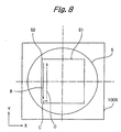
- FIG. 8 An actual wafer inspection was performed by using the above-described electron beam inspection system according to this embodiment.
- Fig. 8 first, the top left inspection starting point S2 in a wafer inspection region S1 of about 130 mm by 130 mm was moved to the center of a region for irradiation with the electron beam 1021. Thereafter, the X-Y stage 1006 was moved in the +Y direction at 10 mm/sec. to inspect the wafer S. Consequently, the wafer inspection region S1 was inspected in the direction of the arrow B. Next, the X-Y stage 1006 was moved in the -X direction to step by about 500 microns. Consequently, the wafer inspection region S1 was shifted in the direction of the arrow C.
- the X-Y stage 1006 was moved in the -Y direction to inspect the wafer S.
- the wafer inspection region S1 was inspected in the direction of the arrow D. In this way, scanning was repeated to inspect the whole wafer inspection region S1.
- the stage speed varied cyclically, showing a deviation of the order of ⁇ 10%, with a period of 2.5 milliseconds.
- the line rate having a frequency in the neighborhood of 300 kHz was cyclically oscillated synchronously with the stage speed variations by the line rate control unit 53, whereby a blur-free, favorable image was obtained.
- the electron beam inspection system according to this embodiment relates to a multi-purpose electron beam inspection system.
- the image projection type electron beam inspection system has a single electron beam irradiation unit.
- a Wien filter E ⁇ B filter
- the intensities of the electric and magnetic fields in the Wien filter are so set that the obliquely applied electron beam is deflected so as to be incident perpendicularly or normally on the sample surface, whereas secondary electrons from the sample are taken out in a direction perpendicular to the sample surface without being deflected.
- Fig. 10 is a block diagram showing the arrangement of an image projection type electron beam inspection system 2034 according to the related art.
- the electron beam inspection system 2034 has an electron gun 2001 for applying a primary electron beam 2102 to a sample 2110, a detector 2114 for detecting secondary electrons 2111 emitted from the sample surface by irradiation with the primary electron beam 2102 and generating an image signal, a Wien filter 2105 having electrodes 2106 and magnets 2107, a first lens system 2003 and a second lens system 2004 for shaping the primary electron beam 2102, a third lens system 2108 and a fourth lens system 2109 positioned between the Wien filter 2105 and the sample 2110, and a sixth lens system 2112 and a seventh lens system 2113 positioned between the Wien filter 2105 and the detector 2114.
- the Wien filter 2105 is set so as to deflect the primary electron beam 2102 emitted from the electron gun 2001 but allow the secondary electrons 2111 emitted from the sample surface to travel straight.
- the Wien filter 2105 makes the primary electron beam 2102 incident perpendicularly or normally on the sample surface.
- This type of system is disclosed, for example, in Japanese Patent Application Unexamined Publication (KOKAI) No. Hei 11-132975.
- the above-described electron beam inspection system is a single-purpose system. As the wafer size increases from 8 inches through 12 inches to 15 inches, the floor area of the electron beam inspection system becomes larger. Moreover, because of the need to perform various inspecting and measuring operations, the proportion of the floor area occupied by the electron beam inspection system in the clean room of semiconductor production facilities increases unfavorably.
- the image projection type electron beam inspection system for defect inspection is a multi-purpose electron beam inspection system for inspecting the condition of the surface of a sample by irradiating a primary electron beam to the sample and detecting secondary electrons emitted from the sample surface.
- the multi-purpose electron beam inspection system has an electron source for generating a primary electron beam, a lens system for shaping the primary electron beam, an optical system for directing the primary electron beam for scanning, a sample stage for supporting a sample, and an optical system for directing secondary electrons toward a detector, and the detector for detecting the secondary electrons to generate an image signal.
- the multi-purpose electron beam inspection system further has at least two functions selected from among defect detection on the sample surface, defect review on the sample surface, pattern line width measurement, and pattern electric potential measurement. The two functions may be the sample surface defect detection and the sample surface defect review.
- the sample surface defect detection may be effected by comparing an image obtained from the image signal with pattern data or by comparing the images of dice with each other.
- the sample surface defect review may be performed by observation of an image on a monitor obtained by beam scanning synchronized with the scanning of the primary electron beam over the wafer surface.
- the pattern line width measurement may be made on the basis of a secondary electron image obtained when the primary electron beam is directed for scanning over the wafer surface in the direction of the short side of a pattern.
- the pattern electric potential measurement may be carried out in such a manner that a negative electric potential is applied to the electrode closest to the sample surface, whereby secondary electrons emitted from a pattern on the sample surface that has a high electric potential are selectively driven back toward the sample.
- the multi-purpose electron beam inspection system inspects the condition of the surface of a sample by applying a primary electron beam to the sample and detecting secondary electrons emitted from the sample surface.
- the multi-purpose electron beam inspection system has a lens system capable of shaping the primary electron beam into at least two configurations selected from among rectangular, circular and spot-shaped configurations, a primary electron optical system having a deflection system for moving the electron beam in a desired direction for scanning, and a detection system for directing secondary electrons emitted from the sample surface toward a detector.
- the multi-purpose electron beam inspection system has the function of automatically detecting a possible defect and the function of outputting information concerning the position of a detected defect and further has the function of allowing observation of the configuration of the defect.
- the detection system may include an image projection optical system. Further, the detection system may include a secondary electron multiplier.
- a plurality of multi-purpose electron beam inspection systems may be combined together as follows.
- a group of multi-purpose electron beam inspection systems may be disposed in one or more lines.
- the group of multi-purpose electron beam inspection systems may share a common sample stage and inspect a sample on the common sample stage.
- Each of the multi-purpose electron beam inspection systems may be arranged toirradiate a plurality of primary electron beams to a sample. Such a combination makes it possible to increase the throughput (the number of samples inspected per unit time) at the inspection step.
- Fig. 11 is a schematic view showing a multi-purpose electron beam inspection system 2030.
- the multi-purpose electron beam inspection system 2030 has a optical column 2028 containing an electron gun 2001 for generating a primary electron beam 2102.
- the multi-purpose electron beam inspection system 2030 further has a shield casing 2029 covering the lower part of the optical column 2028.
- the shield casing 2029 accommodates a wafer (sample) 2110.
- the shield casing 2029 is communicated with the lower part of the optical column 2028 and evacuated to create a vacuum therein as in the case of the inside of the optical column 2028.
- the optical column 2028 contains, in addition to the electron gun 2001, condenser lenses 2002, 2003 and 2004 for irradiating the primary electron beam 2102 to the surface of the wafer 2110, a rectangular aperture 2005, a circular aperture 2006, a deflector 2007, a Wien filter 2009, lens systems 2012, 2010, 2015 and 2017 acting on secondary electrons emitted from the surface of the wafer 2110 irradiated with the primary electron beam 2102, a microchannel plate 2018, a scintillator 2018', and an optical fiber bundle 2019.
- the shield casing 2029 needs magnetic shielding.
- the shield casing 2029 can dispense with magnetic shielding.
- the primary electron beam 2102 emitted from the electron gun 2001 is irradiated to the surface of the wafer (sample) 1110 through the condenser lenses 2002, 2003 and 2004, the rectangular aperture 2005, the circular aperture 2006, the lenses 2024 and 2025, the deflector 2007, the Wien filter 2009, and so forth.
- the primary electron beam 2102 emitted from the electron gun 2001 is converged through the condenser lenses 2002, 2003 and 2004 and is incident to the rectangular aperture 2005 or the circular aperture 2006 behind it with a uniform intensity.
- a demagnified image of the rectangular aperture 2005 or a demagnified image of the circular aperture 2006 or a demagnified crossover image can be selectively formed on the surface of the wafer 2110 by adjusting the lenses 2024 and 2025.
- the wafer surface can be scanned with the primary electron beam 2102 by activating the deflector 2007.
- an image of the wafer surface is produced as follows. Secondary electrons emitted from the surface of the wafer 2110 irradiated with the primary electron beam 2102 are focused onto the microchannel plate 2018 through the lens systems 2012, 2010, 2015 and 2017 and converted into an image of light by the scintillator 2018' on the rear side of the microchannel plate 2018. The light image is taken to the outside through the optical fiber bundles 2019 and 2020 and converted into an electric signal by a two-dimensional CCD 2027. Thus, an image is produced. The produced image is compared with pattern data (automatic pattern alignment procedure). Alternatively, images produced at the same positions on adjacent dies (i.e. adjacent chips fabricated on the same wafer) are compared with each other.
- the electron beam inspection system 2030 has the function of the image projection type electron beam inspection system.
- the brightness of a monitor 2023 is modulated as follows.
- a specific voltage is applied to the lens system 2012 adjacent to the surface of the wafer 2110, thereby directing the path 2014 of the secondary electrons toward a secondary electron multiplier 2021 adjacent to the edge of the wafer surface.
- the secondary electrons are multiplied in the secondary electron multiplier 2021 to obtain an electric signal, which is then amplified by an amplifier 2022 to use it for the brightness modulation of the monitor 2023.
- inspection for a defect on the wafer surface may be performed as follows.
- the deflector 2007 is activated to scan the monitor 2023 with the beam synchronously with the scanning of the surface of the wafer 2110 with the primary electron beam 2102.
- the image thus obtained that is, SEM image, and a pattern data image are compared with each other to detect a possible defect on the wafer surface.
- the electron beam inspection system 2030 also has the function of the electron beam inspection system using the scanning electron beam system (SEM system).
- the line width of pattern lines arrayed along the long-side direction of the pattern can be measured on the basis of the secondary electron image obtained by the monitor 2023.
- the pattern electric potential can be evaluated. That is, a negative electric potential is applied to the electrode 2012a closest to the wafer 2110 among the electrodes in the lens system 2012 adjacent to the surface of the wafer 2110, whereby secondary electrons emitted from a pattern on the wafer surface that has a high electric potential are selectively driven back toward the wafer 2110, thereby evaluating the electric potential of the pattern.
- electrical conduction failures opens, shorts, etc.
- the electron beam inspection system 2030 can be switched between the image projection type inspection system and the scanning electron beam type inspection system by operating a controller 2900.
- the multi-purpose electron beam inspection system can perform multi-purpose inspection and measurement, i.e. defect detection, defect review, pattern line width measurement, and pattern electric potential measurement, by itself as stated above. Therefore, it does not occupy a wide floor area in the clean room. Accordingly, an increased number of device fabrication systems can be installed in the clean room. Thus, the clean room can be utilized effectively.
- the electron beam inspection system according to this embodiment is suitable for performing shape observation and defect inspection of high-density patterns having a minimum line width of 0.1 micron or less, with high accuracy and high reliability.
- an image projection type electron beam inspection system operates as follows.
- the surface of a sample is irradiated with a primary electron beam from an electron gun.
- a secondary electron beam generated from the sample by the electron beam irradiation is focused onto a microchannel plate to multiply the secondary electrons.
- the secondary electron beam is converted into light representing the intensity of the secondary electron beam by a scintillator.
- the light is detected and converted into an electric signal by a TDI-CCD.
- the electric signal is synchronized with the scanning of the sample, thereby obtaining continuous images.
- the image projection type electron beam inspection system requires that the stage moving direction should be made coincident with the light-receiving surface array direction of the TDI-CCD with high accuracy.
- the alignment accuracy depends on mechanical accuracy such as processing accuracy at the time of fabrication and assembling accuracy.
- An object of this embodiment is to provide an electron beam inspection system allowing high-precision alignment between the sample scanning direction and the TDI-CCD light-receiving surface array direction, which has heretofore been impossible to attain owing to the dependence on the mechanical accuracy, thereby making it possible to perform shape observation and defect inspection with high reliability.
- the image projection type electron beam inspection system for defect inspection has an electron irradiation unit for irradiating a sample with a primary electron beam, an optical system for optically processing a secondary electron beam generated from the sample by the primary electron beam irradiation to produce an image of the sample, a microchannel plate for receiving the sample image, a CCD for converting the light signal into an electric signal after a scintillator converts the output of the microchannel plate into a light signal, an image display unit for processing the output of the CCD, and a stage for moving the sample which is used to scan the sample. Between the sample and the microchannel plate, a magnetic lens is positioned to rotate the image.
- the magnetic lens may be positioned between a lens in the final stage of the optical system and the microchannel plate.
- the magnetic lens may be disposed at the crossover position closest to the microchannel plate.
- the magnetic lens may be disposed at the image-formation position closest to the final-stage lens on the side of the final-stage lens remote from the microchannel plate.
- Fig. 12 is a diagram schematically showing the arrangement of the electron beam inspection system according to this embodiment.
- the electron beam inspection system is implemented as an image projection type electron beam inspection system.
- the electron beam inspection system has an electron gun 3001.
- a primary electron beam 3002 emitted from the electron gun 3001 is shaped through a rectangular aperture and enters a Wien filter 3007 having electrodes 3005 and magnets 3006 through lenses 3003 and 3004 arranged in two stages.
- the primary electron beam 3002 is focused onto the plane of the Wien filter 3007 as a rectangular primary electron image having a size of 1 mm by 0.25 mm, for example.
- the optical axis of the primary electron beam 3002 is deflected by the Wien filter 3007.
- the primary electron beam 3002 passes through lenses 3008 and 3009, thereby being reduced to 1/5 in size. Thereafter, the primary electron beam 3002 is irradiated perpendicularly or normally onto a sample 3010 on a stage S.
- the sample 3010 is a wafer, for example, which has circuit patterns formed on the surface thereof.
- Irradiation with the primary electron beam 3002 causes a secondary electron beam 3011 to be emitted from the surface of the sample 3010.
- a part of the primary electron beam 3002 is reflected at the surface of the sample 3010.
- the reflected electron beam and the secondary electron beam 3011 contain information representing a circuit pattern on the sample 3010.
- the secondary electron beam 3011 passes through the lenses 3009 and 3008 and travels straight through the Wien filter 3007. Then, the secondary electron beam 3011 travels along a path off the path of the primary electron beam 3002 and passes through lenses 3012 and 3013 of an electrostatic lens system.
- the secondary electron beam 3011 is magnified by the lenses 3009, 3008, 3012 and 3013.
- the secondary electron beam 3011 emerging from the final-stage lens 3013 of the electrostatic lens system passes through a magnetic lens 3014 before being focused onto a microchannel plate 3015 as a rectangular image.
- the reason why the magnetic lens 3014 is provided will be described later.
- the rectangular image thus formed is intensified 10,000 times by the microchannel plate 3015 to irradiate a fluorescent unit 3016. Consequently, the fluorescent unit 3016 converts the intensified rectangular image into light.
- the light thus obtained passes through a relay optical system 3017 to be applied to a TDI-CCD 3018.
- the TDI-CCD 3018 converts the incident light into an electric signal synchronized with the scanning speed at which the sample 3010 is scanned by the moving stage and gives the electric signal to an image processing unit 3019 as a continuous image.
- the image thus acquired by the image processing unit 3019 is used to detect a possible defect on the surface of the sample 3010 by on-time comparison between the images of a plurality of cells or comparison between the images of a plurality of dice.
- the configurational feature of a defect on the sample 3010 detected in the image processing unit 3019 and the number of defects detected, together with the coordinates of defect locations, etc., are displayed on a CRT and also recorded as the occasion demands.
- various films e.g. an oxide film and a nitride film
- the operating principle of the magnetic lens 3014 shown in Fig. 12 is explained by using Figs. 13(A) and 13(B).
- the magnetic lens 3014 has an annular configuration as seen from above, and its cross-section has U-shaped configurations at the left and right ends thereof.
- Figs. 13(A) and 13(B) show only the central portion of the magnetic lens 3014.
- a magnetic path is formed to extend through the upper pole piece 3021a and the lower pole piece 3021b by an annular coil (not shown) provided between the upper and lower pole pieces 3021a and 3021b.
- a magnetic field is applied to the secondary electron beam 3011.
- This causes the secondary electron beam 3011 to be rotated in the direction indicated by the arrow 3022 with respect to the center of the optical axis of the secondary electron beam 3011.
- the amount of rotation of the secondary electron beam 3011 increases as the magnetic field applied to the secondary electron beam 3011 through the pole pieces 3021a and 3021b is intensified.
- the above-described principle may be utilized as follows.
- the magnetic lens 3014 is positioned between the lens 3013 and the microchannel plate 3015, for example, and the intensity of the magnetic field produced by the magnetic lens 3014 is controlled. By doing so, it is possible to rotate the image formed on the microchannel plate 3015 by the secondary electron beam 3011 emitted from the sample 3010. Accordingly, controlling the intensity of the magnetic field produced by the magnetic lens 3014 allows the scanning direction of the sample 3010 as scanned by the moving stage S to coincide with the integration direction on the light-receiving surface of the TDI-CCD 3018.
- the magnetic lens 3014 is positioned between the lens 3013 in the final stage of the electrostatic lens system and the microchannel plate 3015, the secondary electron beam 3011 and hence the image formed on the microchannel plate 3015 can be rotated by the magnetic lens 3014 without exerting any effect on the electrostatic lens system (e.g. an undesired change in the magnification of the electrostatic lens system, or introduction of aberration or distortion into the image).
- the above-described magnetic lens 3014 should be provided at the position shown in Fig. 14 or 15.
- the magnetic lens 3014 is positioned at the crossover position 3031 closest to the final-stage lens 3013 of the electrostatic lens system between the lens 3013 and the microchannel plate 3015, as has been stated above.
- This arrangement makes it possible to utilize the action of the magnetic lens 3014 to rotate the secondary electron beam 3011. Moreover, the influence on the focusing conditions of the electrostatic lens system in the image projection system can be reduced to a substantially ignorable level.
- the magnetic lens 3014 is provided at the image-formation position 3041 closest to the final-stage lens 3013 of the electrostatic lens system on the side of the lens 3013 remote from the microchannel plate 3015.
- the image-formation position 3041 is conjugate to the surface of the sample 3010 and also to the secondary electron beam incident surface of the microchannel plate 3015.
- the image-formation position 3041 is where no lens action other than the rotating action of the magnetic lens 3014 takes place. Therefore, the magnetic lens 3014 only acts to correct the displacement between the scanning direction of the sample 3010 and the light-receiving surface array direction of the TDI-CCD 3018. In other words, such directional displacement can be corrected easily by the magnetic lens 3014.
- the arrangement shown in Fig. 15 can attain a high degree of accuracy, which is equal to or higher than the accuracy obtained by the arrangement shown in Fig. 14.
- the present embodiment allows the sample scanning direction and the light-receiving surface array direction of the TDI-CCD to be readily aligned with each other. Therefore, it is possible to eliminate or minimize the image blur due to discrepancy between the two directions. Thus, it becomes possible to effect shape observation and defect inspection with high reliability at excellent resolution, i.e. 0.1 micron or less.
- TDI-CCD even if the number of stages of the TDI-CCD is increased, image blur as caused by discrepancy between the sample scanning direction and the TDI-CCD light-receiving surface array direction is minimized. Therefore, it is possible to use a TDI-CCD with an increased number of stages and hence possible to provide an electron beam inspection system exhibiting even higher sensitivity. Accordingly, high throughput can be realized.
- This embodiment relates to an electron beam inspection system that evaluates the surface of a solid sample by using a single or plurality of electron beams. More particularly, the embodiment relates to an electron beam inspection system capable of evaluating samples, e.g. wafers or masks, having patterns with a minimum line width is 0.1 ⁇ m or less, with high throughput (i.e. the number of samples evaluated per unit time), high accuracy and high reliability. Items of evaluation include defect inspection of a sample, e.g. a semiconductor wafer, line width measurement, overlay accuracy measurement, voltage contrast measurement at high time resolution, and so forth. The voltage contrast measurement allows inspection for an electrical defect under the wafer surface and measurement of small particles on the wafer surface.
- the dimension D of the electron beam means the diametrical dimension (diameter of diagonal line length) of the electron beam image on the sample surface.
- the spacing between electron beams means the distance between the centers of adjacent electron beam images on the sample surface.
- This type of electron beam inspection system for evaluating defects on a sample is disclosed, for example, in Japanese Patent Application Unexamined Publication (KOKAI) No. Hei 9-311112.
- This publication discloses a pattern inspection system in which a primary electron beam is applied to a sample formed with a pattern, e.g. a mask or a wafer, and secondary electrons emitted from the sample are used to inspect the pattern on the sample.
- a decelerating electric field is applied between an objective and the sample to narrow down the primary electron beam and the sample is irradiated with the narrowed electron beam, thereby efficiently detecting secondary electrons emitted from the sample.
- the related art uses a secondary electron energy filter comprising a hemispheric mesh electrode to measure the electric potential contrast of the pattern on the sample surface.
- a decelerating electric field type objective used in the above-described related art allows all secondary electrons to pass through it. This makes it difficult to measure the voltage contrast.
- the secondary electron filter comprising a hemispheric mesh electrode has the following problems: If the mesh electrode is provided between the objective and the sample, the image plane distance of the objective lens increase, and the axial chromatic aberration coefficient increases. In addition, the primary electron beam cannot be focussed, or the beam current decreases as the primary electron beam is narrowed down. Further, the mesh electrode irregularly bends the path of the primary electron beam passing near the mesh electrode. Therefore, the beam may be blurred, or scanning distortion may occur.
- an object of this embodiment is to provide an electron beam inspection system capable of obtaining a large beam current while narrowing down the primary electron beam and hence capable of measuring the voltage contrast and free from scanning distortion.
- the electron beam inspection system uses a unipotential electrostatic lens having at least three axially symmetric electrodes: an electrode closer to the electron gun (i.e. upper electrode); an electrode closer to the sample (i.e. sample-side electrode, or lower electrode); and a center electrode between the upper and lower electrodes.
- an electrode closer to the electron gun i.e. upper electrode
- an electrode closer to the sample i.e. sample-side electrode, or lower electrode
- a center electrode between the upper and lower electrodes With the electrostatic lens, a primary electron beam is focused onto the sample surface, and the sample surface is scanned with the primary electron beam by using a deflector. Secondary electrons emitted from the sample by the primary electron beam irradiation are detected to evaluate the sample surface.
- the electron beam inspection system applies a voltage lower than the electric potential at the sample surface to the lower electrode, thereby obtaining the electric potential contrast of the pattern on the sample surface.
- the voltage applied to the electrode of the electrostatic lens that is closer to the electron gun than the center electrode i.e. the voltage applied to the upper electrode
- a contrast image is obtained from changes in the emission of secondary electrons from the sample surface under application of an electric potential distribution.
- Fig. 16 is a diagram schematically showing the arrangement of the electron beam inspection system according to this embodiment.
- an electron gun 4020 has a cathode 4022 placed in a Wehnelt cylinder 4021 and an anode 4023 provided below the Wehnelt cylinder 4021.
- a primary electron beam is emitted from the cathode 4022 toward the anode 4023.
- the electron beam is aligned by aligning deflectors 4024 and 4025 so as to pass through the centers of condenser lenses 4034, 4035 and 4036.
- the primary electron beam emitted from the cathode 4022 is controlled by the condenser lenses 4034, 4035 and 4036 to adjust the image-formation magnification at the sample surface.
- the controlled primary electron beam 4016 is focused onto the surface of a sample 4033 by objective lenses 4032, 4038 and 4039.
- the primary electron beam 4016 forms a crossover image on the deflection center plane of an E ⁇ B separator 4030.
- the primary electron beam 4016 is deflected in two stages by an electrostatic deflector 4027 and an electromagnetic deflector 4029 in the E ⁇ B separator 4030 to raster-scan over the surface of the sample 4033.
- inspection of the sample 4033 is performed by scanning a predetermined width of the surface of the sample 4033 in the x-direction (direction perpendicular to the plane of Fig. 16) with the primary electron beam and, while doing so, continuously moving a stage 4041 in the y-direction.
- the stage 4041 is moved in the x-direction by a predetermined width or by a width slightly larger than the predetermined width to inspect a neighboring stripe (a region adjacent to the predetermined region).
- secondary electrons are emitted from the scanning points on the sample 4033.
- Secondary electrons emitted from the irradiated points on the sample 4033 are extracted toward the electron gun 4020 by an accelerating electric field for the secondary electrons that is formed by the high voltage applied to the center electrode 4039 of the objective 4031 and the ground potential at the upper electrode 4038 and the lower electrode 4032, together with the negative high voltage applied to the sample 4033.
- the secondary electrons are deflected from the primary optical system by the E ⁇ B separator 4030 so as to travel along the path in the direction indicated by the dotted line 18 in Fig. 16. Then, the secondary electrons are detected with a secondary electron beam detector 4028, and thus an SEM image (scanning electron microscope image) is formed.
- a voltage lower than the electric potential at the sample 4033 is applied to the sample-side electrode 4032 of the objective 4031, thereby making the axial potential distribution lower than the potential at the sample surface as shown in Fig. 18 (described below).
- a controller 4900 shown in Fig. 16 allows a desired voltage to be applied to each of the upper electrode 4038, the center electrode 4039 and the lower electrode 4032.
- Fig. 18 shows the distribution of axial potential when 4.5 kV, 8 kV, 350 V and 500 V are applied to the upper electrode 4038, the center electrode 4039, the lower electrode 4032 and the sample 4033, respectively.
- the abscissa axis represents the distance along a Z-axis, i.e. an axis extending perpendicularly to the surface of the sample 4033.
- the point of 0 mm, as a fiducial point, is the intersection between the axis and a line extending from the upper electrode 4038 at right angles to the axis. Accordingly, 4.000 mm in the figure shows the distance from the intersection.
- Fig. 18 shows the distribution of axial potential when 4.5 kV, 8 kV, 350 V and 500 V are applied to the upper electrode 4038, the center electrode 4039, the lower electrode 4032 and the sample 4033, respectively.
- the abscissa axis represents the distance along a Z-axis, i.e.
- the sample 4033 (not shown in the figure) is placed at a position corresponding to the point 4002, and the lower electrode 4032 (not shown in the figure) is provided at a position corresponding to the middle between the point 4001 and the point 4002.
- the center electrode 4039 is provided at a position corresponding to the point 4003. Because a voltage lower than the sample potential is applied to the lower electrode 4032, the axial potential is lower than the electric potential at the surface of the sample 4033 over the range of from the point 4001 to the point 4002.
- the secondary electrons those emitted from a pattern having a high electric potential have low potential energy and hence low speed. Therefore, such secondary electrons are driven back toward the sample 4033 by the potential barrier between the point 4001 and the point 4002. Accordingly, these secondary electrons are not detected.
- secondary electrons emitted from a pattern having a low electric potential have high potential energy and hence high speed. Therefore, these secondary electrons pass the potential barrier and reach the detector 4028.
- the spacing between the center and lower electrodes 4039 and 4032 should preferably be set wider than the spacing between the upper electrode 4038 and the center electrode 4039. Further, the large electric field formed between the center electrode 4039 and the lower electrode 4032 causes the lens action to become excessively strong, resulting in a large deviation of the focusing conditions. To correct the deviation, the positive high voltage applied to the center electrode 4039 should be lowered to a considerable extent.
- Fig. 17 shows the way in which optical column 4040 with a reduced outer diameter are arranged in two rows each consisting of four optical column. In the example shown in Fig. 17, eight optical column 4040 are positioned above an 8-inch wafer in such a manner that each secondary electron beam detector 4028 is directed to a side where it will not interfere with neighboring optical systems.
- optical column 4040 (each having an outer diameter of 40 mm or less, for example) arranged as shown in Fig. 17 and moving the sample stage 4041 in the y-direction, it is possible to obtain throughput (i.e. the number of samples processed per unit time) 8 times as high as that in the case of using a single optical column 4040.
- the secondary electron detection efficiency should preferably be increased.
- an electric potential close to the ground potential should be applied to the sample-side electrode 4032.
- a positive high voltage is applied to the center electrode 4039.
- the voltage applied to the upper electrode 4038, which is close to the ground potential is controlled. In this case, the control voltage can be changed at high speed.
- the electron beam inspection system according to this embodiment has been described as a scanning electron beam (SEM) type inspection system, it should be noted that the featuring portions of this embodiment are also applicable to an image projection type electron beam inspection system.
- SEM scanning electron beam
- a voltage lower than the electric potential at the sample surface is applied to the sample-side electrode of an electrostatic lens having three axially symmetric electrodes, whereby the electron beam inspection system is made free from the problems that the image plane distance of the objective lengthens and hence the axial chromatic aberration coefficient increases, and that the primary electron beam cannot be narrowed down.
- the primary electron beam is kept focused onto the sample surface by varying the positive high voltage applied to the center electrode.
- a voltage close to the ground potential is applied to the sample-side electrode. By doing so, the detection of secondary electrons can be performed efficiently.
- This embodiment relates to a charged particle beam system for applying an electron beam as a charged particle beam to a sample placed on a two- or three-dimensionally movable stage (hereinafter referred to as simply "stage") and also relates to a method of conveying a sample to the stage.
- stage two- or three-dimensionally movable stage
- the whole stage is installed in a vacuum container because of the necessity to place the whole charged beam path in a vacuum environment. Further, in order to allow the stage to function in a vacuum, it is necessary to give special consideration to the support structure and lubrication for the actuator and guide mechanism of the stage, the material of the stage, and so forth, unlike an arrangement in which the stage is operated in the atmospheric environment.
- the actuator for example, when a servomotor is placed in a vacuum, it needs to be designed to meet high-temperature specifications because it is difficult to effect heat dissipation under vacuum. It is also necessary to impose restrictions on the use conditions of the servomotor and to use a solid lubricant or vacuum grease for lubrication of the rotating shaft. When the servomotor is placed on the atmosphere side, it is necessary to provide a vacuum seal mechanism, e.g.
- a magnetic fluid seal in the rotation inlet part and to provide the stage with another guide in addition to an X-direction guide and a Y-direction guide to thereby construct a structure in which the servomotor need not move together with the X-direction guide or the Y-direction guide. Consequently, the structure is complicated and large in size in comparison to the stage operating in the atmospheric environment.
- an air bearing utilizing hydrostatic pressure as used for a high-precision stage used in the atmospheric environment cannot be used under vacuum environmental conditions.
- a high-precision rolling bearing e.g. a cross rolling bearing
- vacuum grease or a fluorine-containing lubricant of low vapor pressure which are inferior in lubricating properties to lubricants used in the atmospheric environment.
- the stage mechanism for use in a vacuum requires the following constituent elements in addition to those stated above: a vacuum container for containing the stage; a load-lock chamber for transferring a sample from an atmospheric environment to a vacuum environment; a vacuum transfer mechanism for conveying the sample under vacuum; vacuum piping for the vacuum container; valves; and a vacuum pump.
- a vacuum chuck which uses suction force, cannot be used as a device for holding the sample. Accordingly, it has heretofore been necessary to use an electrostatic chuck or a mechanical chuck that holds the rear surface or side of the sample with a holding member.
- the electrostatic chuck has problems that it is costly and likely to adsorb particles, and that a certain type of electrostatic chuck requires time to effect destaticization.
- the mechanical chuck is incapable of holding the sample flat and needs to hold the rear surface or side of the sample with a holding member. Therefore, the mechanical chuck cannot meet the semiconductor manufacturers' demands that the chuck should not be brought into contact with any portion of the wafer, as a sample, other than the back thereof.
- the charged particle beam system requires that the stage should be provided in a vacuum environment. Therefore, the system suffers a high production cost and requires a large installation area and occupied area. Further, the mechanism is complicated, and the maintenance of the system is difficult.
- the conventional system also has a problem that processing cannot be carried out with the desired performance. Accordingly, it has been demanded that the amount of gas released from the sample surface and the surfaces of components of the stage into the charged particle beam irradiation area should be reduced to a considerable extent and the released gas should be evacuated rapidly.
- An purpose of this embodiment is to allow a charged particle beam system to be produced in a compact structure and at reduced costs by providing mechanical structures such as the actuator and guide mechanism of the stage in the atmospheric environment.
- Another purpose of this embodiment is to prevent the sample and the charged particle beam optical system from being contaminated with particles or released gas by arranging the charged particle beam system such that only a place where a vacuum environment is required, i.e. where the sample and charged particle beam optical system are placed, is maintained under vacuum.
- a further purpose of this embodiment is to provide a charged particle beam system designed so that the amount of gas released into a vacuum from the sample surface and the surfaces of the stage components can be reduced to a considerably smaller value than in the case of the conventional system.
- a still further purpose of this embodiment is to provide a method of conveying a sample to the inside of a charged particle beam system designed so that the amount of gas released into a vacuum from the sample surface and the surfaces of the stage components can be reduced considerably in comparison to the conventional system.
- a charged particle beam system irradiate a charged particle beam to the surface of a sample placed on a stage.
- at least one annular differential pumping structure is provided around a region where the charged particle beam is applied, and further a structure for blowing an inert gas onto the sample surface is provided at the outer peripheral side of the differential pumping structure.
- the inert gas blowing structure is formed such that the inert gas blown onto the sample surface will flow mainly radially outward from the charged particle beam irradiation area.
- the pumping operation of the differential pumping unit is facilitated. Consequently, it becomes possible to form a compact differential pumping structure and to use a vacuum pump of small capacity for differential evacuation.
- the differential pumping structure has a differential pumping passage for high vacuum and a differential pumping passage for low vacuum. These differential pumping passages connect to each other at the downstream side of the differential pumping structure to perform evacuation through the same piping at the downstream side of the junction of the pumping passages. At the upstream side of the differential pumping structure, the differential pumping passage for low vacuum offers higher pumping resistance than that of the differential pumping passage for high vacuum. Thus, it is possible to reduce the number of differential pumping passages and/or vacuum pumps and hence possible to attain reductions in size and costs of the charged particle beam system.
- the stage is provided with a mechanism for fine height adjustment so that the surface of the stage extending under the differential pumping structure can be flush with the surface of the sample placed on the stage.
- the gap between the differential pumping unit and the stage is kept constant over the whole movable range of the stage. Therefore, it becomes possible to allow the differential pumping function to operate normally over the whole movable range of the stage.
- either the whole movable range of a stage adapted to move a sample to a predetermined position or the movable range of the sample is always covered with a vacuum container filled with an inert gas.
- the container filled with an inert gas is communicably connected with a vacuum container through a block valve, so that a sample is carried in and out of the inert gas-filled container through the vacuum container.
- the vacuum container is evacuated to a predetermined pressure.
- a high-purity inert gas is introduced into the vacuum container.
- the gate valve is opened, and the sample is placed on the stage in the container filled with the high-purity inert gas.
- a high-purity inert gas is introduced into the vacuum container, and the sample is conveyed to the stage in the high-purity inert gas. Accordingly, when the sample is inserted into the charged particle beam irradiation area and placed in the vacuum environment, only the high-purity inert gas can be released from the sample surface.
- the high-purity inert gas has very small adsorption energy with respect to the surface of an object. Therefore, the high-purity inert gas is released from the sample surface within an extremely short period of time and hence will not degrade the degree of vacuum at the charged particle beam irradiation area. Thus, it is easy to maintain the charged particle beam irradiation area at a high degree of vacuum. It is also possible to minimize the likelihood that the sample surface may be contaminated.
- an inert gas circulating mechanism is provided so that the inert gas blown onto the sample surface is recovered by a vacuum pump and/or compressor and then pressurized so as to be blown onto the sample surface again.
- the high-purity inert gas can be recycled and hence economized.
- the high-purity inert gas is not discharged into the room where the present system is installed, it is possible to eliminate the danger of accident such as suffocation by the high-purity inert gas.
- inert gases usable in this embodiment include nitrogen (N 2 ), argon (Ar), xenon (Xe) and the like.
- Another modification of this embodiment provides a sample transporting method. That is, the method includes the following steps: preparing a charged particle beam system wherein a container filled with an inert gas is connected with a vacuum container through a gate valve, as stated above; inserting a sample into the vacuum container of the charged particle beam system; evacuating the vacuum container to a predetermined pressure; introducing an inert gas into the vacuum container; and opening the gate valve and placing the sample onto a stage in the container filled with the inert gas.
- the method allows the charged particle beam irradiation area to be readily maintained at a high degree of vacuum.
- Another modification provides a wafer defect inspection system designed to inspect the surface of a semiconductor wafer for a defect by making use of the above-descried charged particle beam system or sample conveying method.
- a wafer defect inspection system of high reliability can be produced at reduced costs and requires minimum installation and foot print.
- Another modification provides an exposure system designed to transfer a semiconductor device circuit pattern onto the surface of a semiconductor wafer through exposure by utilizing the above-described charged particle beam system or sample conveying method.
- a charged particle beam exposure system of high reliability can be produced at reduced costs and requires minimum installation and occupied areas.
- Another modification provides a semiconductor manufacturing method that utilizes the above-described charged particle beam system or sample conveying method. Thus, it is possible to attain reductions in cost of the semiconductor fabrication method.
- Fig. 19 is a diagram showing an embodiment of the charged particle beam system, which is an enlarged view of a part of the charged particle beam system.
- Reference numeral 5001 denotes an optical column having a publicly known structure for accommodating an optical system for irradiating a charged particle beam 5050 to a sample 5002. Only the distal end portion of the optical column 5001 is shown in the figure.
- a differential pumping unit 5004 is installed in such a manner as to surround the end portion of the optical column 5001.
- the differential pumping unit 5004 has a hole 5041 in the center thereof.
- the hole 5041 needs to be sufficiently large to pass the charged particle beam 5050 without affecting any influence thereon.
- the sample 5002 is placed on a stage 5003. The sample 5002 moves together with the stage 5003.
- the optical column 5001 is secured to a frame (see Fig. 24) of the system such that a small gap of the order of from several microns to several hundred microns is maintained between the differential pumping unit 5004 and the surface 5021 of the sample 5002 (hereinafter referred to as "sample surface 5021"). It should be noted that the optical system in the optical column 5001 is not the gist of the present invention. Therefore, a detailed description thereof is omitted.
- the differential pumping unit 5004 has annular grooves 5005 and 5006 for differential pumping provided in order from the center toward the radially outer side.
- the annular groove 5005 is communicated with vacuum piping 5008.
- the annular groove 5006 is communicated with vacuum piping 5009. Gas flowing in toward the charged particle beam 5050 from the outer peripheral side of the differential evacuation unit 5004 is evacuated through the annular grooves 5005 and 5006, whereby the flow rate of gas leaking to the charged particle beam irradiation area is reduced below the allowable level, thereby maintaining the charged particle beam irradiation area at a predetermined degree of vacuum.
- the configuration of the annular groove 5005, the configuration of the evacuation flow path of the annular groove 5005, the gap 5051 between the sample surface 5021 and the differential evacuation unit 5004 and the performances of the vacuum piping and the vacuum pump are determined appropriately so that the annular groove 5005 is higher in the degree of vacuum than the annular groove 5006 and the flow rate of gas leaking to the charged particle beam irradiation area is below the allowable level, or that the annular groove 5005 is higher in the degree of vacuum than the charged particle beam irradiation area.
- Annular grooves for performing differential pumping constitute a differential pumping structure. In Fig. 19, the annular grooves are formed in a concentric double-groove configuration. However, the present invention is not necessarily limited to the double-groove configuration.
- the differential pumping structure may be formed from a single annular groove or three or more concentric annular grooves, depending on the degree of vacuum required at the charged particle beam irradiation area and on the arrangement of the annular grooves, the vacuum piping and so
- annular groove 5007 is formed at the outer peripheral side of the annular groove 5006 of the differential pumping unit 5004.
- the annular groove 5007 is communicated with piping 5010.
- a high-purity inert gas is supplied and blown off from the annular groove 5007 onto the sample surface 5021.
- a part of the high-purity inert gas blown off from the annular groove 5007 is discharged to the charged particle beam irradiation area by suction acting through the annular groove 5006.
- the rest of the high-purity inert gas flows in the opposite direction and is discharged to the outside from the outer periphery of the differential pumping unit 5004.
- the high-purity inert gas flows outward to act as a shield.
- the atmospheric air is prevented from flowing into the charged particle beam irradiation area by the outward flow of the high-purity inert gas. If the shield mechanism effected by the high-purity inert gas is not provided, the outside air flows into the area between the sample surface 5021 and the differential pumping unit 5004. Consequently, particles and water vapor in the atmospheric air may enter the charged particle beam irradiation area and contaminate the sample surface 5021 and the lenses in the optical column 5001, which adversely affects such operations as inspection of the wafer surface using a charged particle beam and transfer of a pattern onto the wafer surface by exposure.
- the provision of a high-purity inert gas blowing mechanism as in the present invention makes it possible to prevent entry of particles and water vapor in the atmospheric air and hence eliminates the likelihood of the sample and the lenses being contaminated. Accordingly, operations such as wafer inspection and exposure can be carried out without any problem.
- Fig. 20 shows a modification of the charged particle beam system.
- a high-purity inert gas outlet 5007a is directed toward the outer peripheral side. Consequently, the gas forcibly flows radially outward in the direction of the arrow A between the sample surface 5021 and the differential pumping unit 5004.
- the high-purity inert gas outlet 5007a is formed as stated above and the high-purity inert gas supply pressure is raised to an appropriate value with respect to the atmospheric pressure to thereby set the velocity of the high-purity inert gas flow from the outlet 5007a to an appropriate value, the flow of the high-purity inert gas acts as an ejector, and a flow such as that indicated by the arrow B occurs.
- the inner peripheral side of the differential pumping unit 5004 can be maintained at a negative pressure.
- contaminants in the outside air e.g. particles and water vapor
- an pumping effect is provided. Accordingly, the load of evacuation on the differential pumping mechanism can be reduced.
- differential pumping unit 5004 may be provided with a baking heater BH to heat the differential pumping unit 5004, whereby the gas flowing from the annular grooves 5005 and 5006 to the vacuum piping 5008 and 5009 is expanded under heating to increase the evacuation efficiency, thereby enabling a high degree of vacuum to be attained by differential evacuation even more easily.
- Fig. 21 shows another modification of the charged particle beam system.
- a vacuum chamber 5011 is provided in the differential pumping unit 5004.
- the vacuum chamber 5011 is communicated with both a high vacuum-side evacuation passage 5005a and a low vacuum-side evacuation passage 5006a.
- a high vacuum-side annular groove 5005 and a low vacuum-side annular groove 5006 for differential evacuation are communicated with the high vacuum-side evacuation passage 5005a and the low vacuum-side evacuation passage 5006a, respectively.
- the vacuum chamber 5011 is held under vacuum through vacuum piping 5008a.
- the low vacuum-side evacuation passage 5006a is formed with an extremely small conductance relative to that of the high vacuum-side evacuation passage 5005a. Accordingly, the downstream-side pressures of the evacuation passages 5005a and 5006a are both equal to the pressure in the vacuum chamber 5011, that is, equal to each other. However, the pressures in the annular grooves 5005 and 5006, which are upstream the evacuation passages 5005a and 5006a, are different from each other to a considerable extent. Thus, the annular groove 5006 maintains a low vacuum, and the annular groove 5005 maintains a high vacuum, thereby allowing differential pumping to be effected appropriately.
- the differential pumping unit 5004 is allowed to dispense with other vacuum piping than the vacuum piping 5008a. Accordingly, it is possible to attain reductions in size and costs of the system.
- Figs. 22(a) and 22(b) show another modification of the charged particle beam system.
- Fig. 22(a) shows a state where the column is positioned in the vicinity of one end of the stage.
- Fig. 22(b) shows a state where the column is positioned in the vicinity of the other end of the stage.
- a sample 5002 is placed on the stage surface 5031, and plate members 5060 and 5061 are mounted around the sample 5002.
- the height of the plate members 5060 and 5061 from the stage surface 5031 has previously been adjusted so that the top surfaces 5601 and 5611 of the plate members 5060 and 5061 are flush with the sample surface 5021.
- the gap 5051' (or 5051") between the differential pumping unit 5004' (or 5004") and the stage surface 5031 or the sample surface 5021 is kept constant at all times even when the stage moves or the position of the column relative to the stage shifts to the position denoted by reference numeral 5001' or 5001" [Fig. 22(a) and Fig. 22(b)]. Therefore, differential pumping can be effected appropriately. Thus, the charged particle beam irradiation area can be maintained at a predetermined degree of vacuum at all times.
- Fig. 23 shows another modification of the charged particle beam system.
- an elevating mechanism 5062 is provided under a sample carrier (in this embodiment, a sample carrier using an electrostatic chuck, for example) 5063 for supporting and holding a sample, which is disposed in a recess 5032 of the stage 5003.
- a sample carrier in this embodiment, a sample carrier using an electrostatic chuck, for example
- the height of the sample surface is adjusted so that the sample surface is flush with the stage surface.
- the height difference should preferably be reduced to the order of submicrons.
- a fine adjustment mechanism using a piezoelectric element or the like may be provided as the elevating mechanism 5062.
- the system may be arranged such that adjusting members 5060' and 5061' are provided at the sides of the sample carrier 5063, and the adjusting members 5060' and 5061' are replaced with others in conformity to the thickness of the sample 5002.
- the adjusting members 5060' and 5061' may comprise either a single component or two or more separate components according to the configurations of the sample 5002 and the stage 5003. It is desirable to arrange the adjusting members 5060' and 5061' and the elevating mechanism 5062 so that even if the sample 5002 changes in size from an 8-inch wafer to a 12-inch wafer, the system can be adapted for any size of the sample 5002 simply by replacing the components in conformity to the sample size.
- Fig. 24 shows another modification of the charged particle beam system.
- a sample 5002 is placed on the stage 5003.
- the sample 5002 moves within a range indicated by reference symbol L (movable range) in association with the movement of the stage 5003.
- the column 5001 is secured to a frame 5014.
- the bottom of the column 5001 is provided with a differential pumping unit 5004 in such a manner that the differential pumping unit 5004 surrounds the bottom of the column 5001.
- Differential pumping and blowing of a high-purity inert gas are carried out in the area between the differential pumping unit 5004 and the sample surface 5021 or the stage surface 5031.
- a container 5012 is mounted above the stage 5003 so as to cover the movable range L of the sample 5002 completely.
- a small gap 5052 is provided between the sample surface 5021 or plate members 5060 and 5061 and the lower end surface of the container 5012.
- the high-purity inert gas blown off from the differential pumping unit 5004 enters the container 5012 through the gap 5051 between the differential pumping unit 5004 and the sample surface 5021 or the plate members 5060 and 5061. Consequently, an amount of gas that is equal to the amount of high-purity inert gas entering the container 5012 blows off to the outside of the container 5012 through the small gap 5052.
- the container 5012 is always filled with the high-purity inert gas, and there is no possibility of the outside air entering the container 5012 through the small gap 5052.
- the inside of the container 5012 is kept clean. Therefore, even when the sample 5002 moves within the container 5012, there is no likelihood of the sample 5002 being contaminated by particles, water vapor, etc. Accordingly, it becomes easy to stabilize the charged particle beam irradiation area at a high degree of vacuum.
- the sample surface 5021 or the lenses in the column 5001 may be contaminated.
- the system can be improved in reliability and operating efficiency.
- Fig. 25 shows another modification of the charged particle beam system.
- a container 5015 is formed so as to completely surround not only the sample movable range but also the stage 5003, unlike the arrangement shown in Fig. 24.
- the high-purity inert gas blown off from the differential pumping unit 5004 is evacuated through a vacuum pipe 5016.
- the arrangement of this modification also provides advantageous effects similar to those of the modification shown in Fig. 24.
- the container 5015 covers the stage 5003 completely, it is possible to completely eliminate the possibility of contaminants such as particles and water vapor entering from the outside. Accordingly, the system can be further improved in reliability and operating efficiency.
- both the container 5012 in Fig. 24 and the container 5015 in Fig. 25 only require to make the pressure therein slightly higher than the atmospheric pressure so that the high-purity inert gas can be evacuated through the gap 5052 or the vacuum pipe 5016. Accordingly, containers having a simple structures such as covers will be sufficient to serve as the containers 5012 and 5015. The provision of the container 5012 or 5015 has only a little effect on the size and costs of the system.
- Fig. 26 shows another modification of the charged particle beam system.
- This modification is provided with a container 5017 that covers the stage 5003 completely and is filled with a high-purity inert gas as in the case of the modification shown in Fig. 25.
- the container 5017 is communicably connected with a vacuum container 5027 for loading and unloading a sample.
- the vacuum container 5027 is connected with vacuum piping 5029 and high-purity inert gas supply piping 5030. Further, a block valve 5028 is provided between the vacuum container 5027 and the container 5017.
- the charged particle beam system according to this modification performs processing by the following method.
- the lid (not shown) of the vacuum container 5027 is opened, and a sample 5002 to be processed with a charged particle beam is inserted into the vacuum container 5027. Then, the lid is closed hermetically, and the vacuum container 5027 is evacuated to a predetermined degree of vacuum through the vacuum piping 5029. Next, a high-purity inert gas is supplied through the supply piping 5030 to fill the vacuum container 5027 with the high-purity inert gas. When the pressure in the vacuum container 5027 has reached the same pressure as that in the container 5017, the gate valve 5028 is moved in the direction of the arrow C to move the sample 5002 into the container 5017.
- the sample 5002 is placed at a predetermined position on the stage 5003 by a sample transfer mechanism (not shown). That is, after the sample 5002 has been inserted into the vacuum container 5027, the vacuum container 5027 is evacuated to a predetermined pressure. Then, a high-purity inert gas is introduced into the vacuum container 5027. Thereafter, the gate valve 5028 is opened, and the sample 5002 is placed on the stage 5003 in the container 5017 filled with the high-purity inert gas. Thereafter, the stage 5003 is moved to carry the sample 5002 to the charged particle beam irradiation area to perform processing with the charged particle beam.
- the sample surface 5021 cleaned by evacuation is covered with a high-purity inert gas at all times during the transfer to the charged particle beam irradiation area. That is, after being cleaned by evacuation, the sample surface 5021 is not exposed to the atmospheric air. Accordingly, even when the sample 5002 is exposed to a vacuum environment again after being carried in the charged particle beam irradiation area, gas that may be released from the sample surface 5021 is only the high-purity inert gas covering the sample surface 5021. Therefore, the released gas is evacuated within an extremely short period of time, and the degree of vacuum at the charged particle beam irradiation area will not be degraded. Thus, it becomes easy to maintain the charged particle beam irradiation area at a high degree of vacuum, and it is also possible to minimize the likelihood that the sample surface 5021 may be contaminated.
- Fig. 27 illustrates an embodiment of the evacuation path of the charged particle beam system.
- piping 5013 for evacuating the column 5001 is connected to an ultrahigh vacuum pump 5018.
- the piping 5008 for high vacuum of the differential pumping unit 5004 is connected to an ultrahigh vacuum pump 5020.
- the piping 5009 for low vacuum is connected to roughing piping of the ultrahigh vacuum pump 5020 and evacuated by a roughing pump 5201.
- nitrogen gas is supplied to the differential pumping unit 5004 from a nitrogen gas source 5022 through piping 5010.
- Fig. 28 illustrates a modification of the evacuation path of the charged particle beam system.
- the piping 5013 for evacuating the column 5001 and the piping 5008 for high vacuum of the differential pumping unit 5004 are joined together and connected to an ultrahigh vacuum pump 5018 so as to be evacuated by the ultrahigh vacuum pump 5018.
- the piping 5009 for low vacuum of the differential pumping unit 5004 is connected to roughing piping of the ultrahigh vacuum pump 5018 and evacuated by a roughing pump 5019.
- ultrahigh vacuum pumps for example, a turbo-molecular pump or an ion pump can be used.
- roughing pumps for example, a dry pump or a diaphragm pump can be used.
- Fig. 29 is a diagram showing another modification of the charged particle beam system, which illustrates an inert gas circulating path.
- a container 5015 filled with a high-purity inert gas is supplied with the high-purity inert gas from a differential pumping unit 5004 provided on a column 5001.
- the supplied high-purity inert gas is evacuated from the container 5015 through a vacuum pipe 5016 and pressurized by a compressor 5023.
- the pressurized high-purity inert gas is sent to a gas purifier 5024, e.g. a cold trap or a high-purity filter, through piping 5025.
- a gas purifier 5024 e.g. a cold trap or a high-purity filter
- the high-purity inert gas is sent to the differential pumping unit 5004 again through piping 5010 and then supplied into the container 5015.
- the gas purifier 5024 need not be provided in a case where the gas can be circulated without deteriorating the purity.
- the high-purity inert gas supplied from the differential pumping unit 5004 is sucked by a differential pumping mechanism and evacuated by an ultrahigh vacuum pump 5020 and a roughing pump 5201 through piping 5009 for low vacuum and piping 5008 for high vacuum.
- Piping 5026 provided at the evacuation side of the roughing pump 5201 is connected to the evacuation-side piping 5025 of the compressor 5023. Therefore, the high-purity inert gas passing through this path is also supplied to the differential pumping unit 5004 again through the piping 5010.
- the high-purity inert gas can be circulated for reuse. Therefore, the high-purity inert gas can be economized. Further, because the high-purity inert gas is not discharged into the room where the present system is installed, it is possible to eliminate the danger of accident such as suffocation by the inert gas.
- an electron beam E emitted from an electron gun 5071 in a column 5070 for a primary optical system passes through a lens unit 5072, thereby being shaped into a predetermined sectional configuration.
- the shaped electron beam (charged particle beam) 5050 enters a Wien filter 5073.
- the Wien filter 5073 deflect the path of the electron beam 5050 so that the electron beam 5050 is incident perpendicularly or normally on the surface of a wafer 5002 as a sample under inspection.
- secondary electrons are emitted from the sample surface.
- the secondary electrons are accelerated by an objective 5074 and travel straight through the Wien filter 5073. Thereafter, the secondary electrons are magnified and map-projected onto a detector 5076 by a lens unit 5075.
- the detector 5076 produces a projected image of secondary electrons.
- the image is subjected to image processing and, if necessary, compared with an image of another inspection region, thereby judging whether or not there is a defect on the wafer surface.
- the result of the judgment is recorded in a given device by a predetermined method and also displayed on a given device.
- a differential pumping unit 5004 a container 5015, vacuum piping 5008 and 5009, high-purity inert gas supply piping 5010, etc. are the same as those in the embodiments described above in connection with Figs. 19 to 29.
- the high-purity inert gas flows through the container 5015 as indicated by the arrow D in the figure and is evacuated through a vacuum pipe 5016.
- This embodiment provides the following advantageous effects:
- Fig. 31 is a flowchart showing an embodiment of the semiconductor device fabrication method according to the present invention.
- the fabrication process of this embodiment includes the following main steps:
- each of the above-described main steps further includes some sub-steps.
- the wafer processing step (3) exerts a decisive influence upon the performance of the resulting semiconductor devices.
- designed circuit patterns are stacked successively on the wafer to form a multiplicity of chips operating as memories or MPU's.
- the wafer processing step includes the following steps:
- the wafer processing step is repeated the number of times equal to the number of necessary layers to produce semiconductor devices that are operable as designed.
- Fig. 32 is a flowchart showing the lithography step, which is at the core of the wafer processing step in Fig. 31.
- the lithography step includes the following steps:
- defect inspection method and defect inspection system according to the present invention allows even semiconductor devices having fine patterns to be inspected with favorably high throughput. Accordingly, it becomes possible to perform 100% inspection and hence possible to improve the product yield and to prevent shipment of defective products.
- the electron beam defect inspection system is used after an important fabrication step that is considered to be most in need of inspection [e.g. etching, film deposition (including plating), or CMP (Chemical/Mechanical Polishing) planarization treatment].
- a wafer to be inspected is carried to an ultraprecision X-Y stage through an atmosphere transfer system and a vacuum transfer system and aligned on the stage. Thereafter, the wafer is secured by an electrostatic chuck mechanism or the like and then subjected to defect inspection or other processing according to the following procedure (i.e. the inspection flow shown in Fig. 33).
- the confirmation of the position of each die and the detection of the height of each position are performed according to need with an optical microscope, and information thus obtained is stored in a memory (step 7001).
- the optical microscope acquires an optical microscopic image of a region where defect inspection or the like is to be performed. The image thus obtained is used for comparison with an electron beam image.
- step 7002 information concerning a recipe is selected according to the type of inspection and the type of wafer (e.g. according to which step has been carried out just before the present inspection step, and whether the wafer size is 20 cm or 30 cm) and input to the system (step 7002). Then, designation of an inspection position (step 7003), setting of the electron optical system and setting of inspection conditions, and so forth are made (step 7004). Thereafter, a defect inspection is carried out in real time under normal circumstances while image acquisition is being performed (step 7005). Thus, inspection based on cell-to-cell comparison, die-to-die comparison, etc. is performed by a high-speed information processing system having an algorithm, and the result of the inspection is output to a CRT or the like and stored in a memory according to need (step 7006).
- Defects include particle defects, shape abnormalities (pattern defects), and electrical defects (disconnection and conduction failures of wiring patterns or vias, etc.).
- the system can also automatically distinguish between these defects and classify defect sizes and killer defects (serious defects that make the chip impossible to use) in real time.
- the detection of electrical defects is effected by detecting a contrast abnormality. For example, a conduction failure position is charged positively by electron beam irradiation (about 500 eV) under ordinary circumstances and consequently reduced in contrast. Therefore, it can be distinguished from a normal position.
- Electron beam irradiation devices used in this case include, in addition to an electron beam irradiation device for ordinary inspection, an electron beam emitter (a thermionic emitter or a UV/photoelectron emitter) for emitting an electron beam of low energy provided to enhance the contrast by an electric potential difference.
- an electron beam emitter a thermionic emitter or a UV/photoelectron emitter
- the electron beam of low energy is emitted and irradiated to the region under inspection.
- a conduction failure position can be charged positively by irradiation with the electron beam for inspection. Therefore, in such a case, the device for generating an electron beam of low energy need not additionally be provided, depending upon the specifications.
- a portion that should be electrically insulated shows a difference in the electric potential measured when the portion is electrically insulated or when it is conducting.
- an electric charge is given to the sample in advance so that there is a difference in electric potential between a portion that should be electrically insulated and a portion that should be electrically insulated but is conducting for some reason.
- a beam is applied to the sample by the method according to the present invention, thereby obtaining data containing the electric potential difference.
- the data thus obtained is analyzed to detect the fact that the portion that should be electrically insulated is conducting.
- a target substance when an electron beam is generated, a target substance is floated by the proximity interaction (electrification of particles near the surface) and drawn to a high-electric potential area. Therefore, an organic material acting as an insulating material is deposited on the surfaces of various electrodes used to form and deflect the electron beam.
- the insulating material gradually deposited on the surface of an electrode as the electrode surface is electrically charged has an adverse effect on the formation of the electron beam or on the deflecting mechanism. Therefore, the deposited insulating material has to be removed periodically. Periodic removal of the deposited insulating material is carried out as follows. A plasma of hydrogen, oxygen, fluorine, or a compound containing such a substance, e.g.
- HF, O 2 , H 2 O, or C m F n is produced in a vacuum by utilizing an electrode in the vicinity of an area where the insulating material is deposited, and the plasma electric potential in the space is maintained at an electric potential at which sputtering occurs on the electrode surface (several kV, e.g. 20 V to 5 kV), thereby removing only organic substances by oxidation, hydrogenation, or fluorination.
- inspection means not only the detection of presence of failures, e.g. defects, but also the evaluation of the inspection result.
Landscapes
- Chemical & Material Sciences (AREA)
- Analytical Chemistry (AREA)
- Testing Or Measuring Of Semiconductors Or The Like (AREA)
- Analysing Materials By The Use Of Radiation (AREA)
Applications Claiming Priority (11)
| Application Number | Priority Date | Filing Date | Title |
|---|---|---|---|
| JP2001002722 | 2001-01-10 | ||
| JP2001027222 | 2001-01-10 | ||
| JP2001075865 | 2001-03-16 | ||
| JP2001075865 | 2001-03-16 | ||
| JP2001092748 | 2001-03-28 | ||
| JP2001092748 | 2001-03-28 | ||
| JP2001125349 | 2001-04-24 | ||
| JP2001125349 | 2001-04-24 | ||
| JP2001189325 | 2001-06-22 | ||
| JP2001189325 | 2001-06-22 | ||
| PCT/JP2001/009628 WO2002056332A1 (fr) | 2001-01-10 | 2001-11-02 | Appareil et procede d'inspection a faisceau d'electrons, et procede de fabrication de dispositif comportant l'appareil d'inspection |
Publications (2)
| Publication Number | Publication Date |
|---|---|
| EP1271604A1 true EP1271604A1 (fr) | 2003-01-02 |
| EP1271604A4 EP1271604A4 (fr) | 2005-05-25 |
Family
ID=27531771
Family Applications (1)
| Application Number | Title | Priority Date | Filing Date |
|---|---|---|---|
| EP01978999A Withdrawn EP1271604A4 (fr) | 2001-01-10 | 2001-11-02 | Appareil et procede d'inspection a faisceau d'electrons, et procede de fabrication de dispositif comportant l'appareil d'inspection |
Country Status (4)
| Country | Link |
|---|---|
| US (3) | US6992290B2 (fr) |
| EP (1) | EP1271604A4 (fr) |
| JP (2) | JPWO2002056332A1 (fr) |
| WO (1) | WO2002056332A1 (fr) |
Cited By (2)
| Publication number | Priority date | Publication date | Assignee | Title |
|---|---|---|---|---|
| EP4293699A1 (fr) * | 2022-06-16 | 2023-12-20 | FEI Company | Procédés de détermination de l'emplacement d'une source d'ions métalliques liquides |
| TWI909571B (zh) * | 2023-08-01 | 2025-12-21 | 大陸商北京北方華創微電子裝備有限公司 | 製程腔室的潔淨度檢測方法和製程腔室 |
Families Citing this family (154)
| Publication number | Priority date | Publication date | Assignee | Title |
|---|---|---|---|---|
| JP3534582B2 (ja) * | 1997-10-02 | 2004-06-07 | 株式会社日立製作所 | パターン欠陥検査方法および検査装置 |
| JP2002260296A (ja) * | 2001-02-28 | 2002-09-13 | Sony Corp | 電子ビーム照射装置及び電子ビーム照射方法 |
| US6998611B2 (en) * | 2001-09-06 | 2006-02-14 | Ebara Corporation | Electron beam apparatus and device manufacturing method using same |
| JP3626453B2 (ja) * | 2001-12-27 | 2005-03-09 | 株式会社東芝 | フォトマスクの修正方法及び修正装置 |
| JP3996774B2 (ja) * | 2002-01-09 | 2007-10-24 | 株式会社日立ハイテクノロジーズ | パターン欠陥検査方法及びパターン欠陥検査装置 |
| US6853143B2 (en) * | 2002-01-09 | 2005-02-08 | Ebara Corporation | Electron beam system and method of manufacturing devices using the system |
| FR2838272B1 (fr) * | 2002-04-09 | 2004-07-16 | St Microelectronics Sa | Procede et dispositif de correction de rotation d'un affichage video |
| DE10235456B4 (de) * | 2002-08-02 | 2008-07-10 | Leo Elektronenmikroskopie Gmbh | Elektronenmikroskopiesystem |
| US7157703B2 (en) * | 2002-08-30 | 2007-01-02 | Ebara Corporation | Electron beam system |
| US7015467B2 (en) * | 2002-10-10 | 2006-03-21 | Applied Materials, Inc. | Generating electrons with an activated photocathode |
| US7446474B2 (en) * | 2002-10-10 | 2008-11-04 | Applied Materials, Inc. | Hetero-junction electron emitter with Group III nitride and activated alkali halide |
| US6770895B2 (en) * | 2002-11-21 | 2004-08-03 | Asml Holding N.V. | Method and apparatus for isolating light source gas from main chamber gas in a lithography tool |
| US7012583B2 (en) * | 2003-02-07 | 2006-03-14 | Shimadzu Corporation | Apparatus and method for testing pixels of flat panel display |
| US7135675B1 (en) * | 2003-03-10 | 2006-11-14 | Kla-Tencor Technologies Corporation | Multi-pixel and multi-column electron emission inspector |
| US6919573B2 (en) * | 2003-03-20 | 2005-07-19 | Asml Holding N.V | Method and apparatus for recycling gases used in a lithography tool |
| US7138629B2 (en) | 2003-04-22 | 2006-11-21 | Ebara Corporation | Testing apparatus using charged particles and device manufacturing method using the testing apparatus |
| CN101630623B (zh) * | 2003-05-09 | 2012-02-22 | 株式会社荏原制作所 | 基于带电粒子束的检查装置及采用了该检查装置的器件制造方法 |
| JP2004363085A (ja) * | 2003-05-09 | 2004-12-24 | Ebara Corp | 荷電粒子線による検査装置及びその検査装置を用いたデバイス製造方法 |
| US7248353B2 (en) * | 2003-05-30 | 2007-07-24 | Ebara Corporation | Method and apparatus for inspecting samples, and method for manufacturing devices using method and apparatus for inspecting samples |
| JP4266713B2 (ja) * | 2003-06-03 | 2009-05-20 | キヤノン株式会社 | 位置決め装置及び露光装置 |
| JP2005101537A (ja) * | 2003-08-29 | 2005-04-14 | Canon Inc | 露光装置及びそれを用いたデバイスの製造方法 |
| JP4230880B2 (ja) * | 2003-10-17 | 2009-02-25 | 株式会社東芝 | 欠陥検査方法 |
| WO2005074002A2 (fr) * | 2004-01-29 | 2005-08-11 | Applied Materials Israel, Ltd. | Systeme et procede de focalisation pour systeme d'imagerie de particules chargees |
| US6833717B1 (en) * | 2004-02-12 | 2004-12-21 | Applied Materials, Inc. | Electron beam test system with integrated substrate transfer module |
| US7355418B2 (en) * | 2004-02-12 | 2008-04-08 | Applied Materials, Inc. | Configurable prober for TFT LCD array test |
| US7319335B2 (en) * | 2004-02-12 | 2008-01-15 | Applied Materials, Inc. | Configurable prober for TFT LCD array testing |
| JP2005249745A (ja) * | 2004-03-08 | 2005-09-15 | Ebara Corp | 試料表面検査方法および検査装置 |
| US7448012B1 (en) | 2004-04-21 | 2008-11-04 | Qi-De Qian | Methods and system for improving integrated circuit layout |
| JP4578875B2 (ja) * | 2004-07-16 | 2010-11-10 | 株式会社荏原製作所 | 写像型電子顕微鏡 |
| JP4359232B2 (ja) * | 2004-12-20 | 2009-11-04 | 株式会社日立ハイテクノロジーズ | 荷電粒子線装置 |
| JP2006202654A (ja) * | 2005-01-21 | 2006-08-03 | Horon:Kk | ステージ |
| JP2006216396A (ja) * | 2005-02-04 | 2006-08-17 | Hitachi High-Technologies Corp | 荷電粒子線装置 |
| KR101279028B1 (ko) * | 2005-02-17 | 2013-07-02 | 가부시키가이샤 에바라 세이사꾸쇼 | 전자선장치 |
| TWI415162B (zh) * | 2005-03-03 | 2013-11-11 | Toshiba Kk | 映像投影型電子線裝置及使用該裝置之缺陷檢查系統 |
| US20090014649A1 (en) * | 2005-03-22 | 2009-01-15 | Ebara Corporation | Electron beam apparatus |
| US7535238B2 (en) * | 2005-04-29 | 2009-05-19 | Applied Materials, Inc. | In-line electron beam test system |
| US8067732B2 (en) * | 2005-07-26 | 2011-11-29 | Ebara Corporation | Electron beam apparatus |
| JP4875886B2 (ja) | 2005-11-22 | 2012-02-15 | 株式会社日立ハイテクノロジーズ | 荷電粒子線装置 |
| JP5058489B2 (ja) * | 2006-01-25 | 2012-10-24 | 株式会社荏原製作所 | 試料表面検査装置及び検査方法 |
| JPWO2007086400A1 (ja) * | 2006-01-25 | 2009-06-18 | 株式会社荏原製作所 | 試料表面検査方法及び検査装置 |
| JP4930754B2 (ja) * | 2006-01-25 | 2012-05-16 | エスアイアイ・ナノテクノロジー株式会社 | 荷電粒子ビーム装置 |
| EP1816668A2 (fr) * | 2006-02-01 | 2007-08-08 | FEI Company | Dispositif optique à particules chargées à pression finale prédéterminée |
| JP4825530B2 (ja) * | 2006-02-06 | 2011-11-30 | 株式会社日立ハイテクノロジーズ | パターン欠陥検査方法および装置 |
| WO2007106759A2 (fr) * | 2006-03-14 | 2007-09-20 | Applied Materials, Inc. | Procédé destiné à réduire la diaphonie dans un système de mise à l'épreuve de faisceau électronique multi-colonne |
| JP4734148B2 (ja) | 2006-03-14 | 2011-07-27 | 株式会社日立ハイテクノロジーズ | 試料観察方法,画像処理装置、及び荷電粒子線装置 |
| JP4741408B2 (ja) * | 2006-04-27 | 2011-08-03 | 株式会社荏原製作所 | 試料パターン検査装置におけるxy座標補正装置及び方法 |
| US7602199B2 (en) * | 2006-05-31 | 2009-10-13 | Applied Materials, Inc. | Mini-prober for TFT-LCD testing |
| US7786742B2 (en) | 2006-05-31 | 2010-08-31 | Applied Materials, Inc. | Prober for electronic device testing on large area substrates |
| JP2007335125A (ja) * | 2006-06-13 | 2007-12-27 | Ebara Corp | 電子線装置 |
| US9257257B2 (en) * | 2006-06-30 | 2016-02-09 | Shimadzu Corporation | Electron beam control method, electron beam generating apparatus, apparatus using the same, and emitter |
| US20080073572A1 (en) * | 2006-07-20 | 2008-03-27 | Siegfried Schwarzl | Systems and methods of measuring power in lithography systems |
| JP5139658B2 (ja) * | 2006-09-21 | 2013-02-06 | 株式会社ニューフレアテクノロジー | 描画データ処理制御装置 |
| US20080116390A1 (en) * | 2006-11-17 | 2008-05-22 | Pyramid Technical Consultants, Inc. | Delivery of a Charged Particle Beam |
| DE102006059416B4 (de) * | 2006-12-15 | 2009-05-20 | Fraunhofer-Gesellschaft zur Förderung der angewandten Forschung e.V. | Vorrichtung und Verfahren zur Steigerung der Messgenauigkeit digitaler 3D-Geometriemesssysteme |
| JP2010519697A (ja) * | 2007-02-22 | 2010-06-03 | アプライド マテリアルズ イスラエル リミテッド | 高スループットsemツール |
| JP2008233035A (ja) * | 2007-03-23 | 2008-10-02 | Toshiba Corp | 基板検査方法 |
| US20080251019A1 (en) * | 2007-04-12 | 2008-10-16 | Sriram Krishnaswami | System and method for transferring a substrate into and out of a reduced volume chamber accommodating multiple substrates |
| JP5055015B2 (ja) * | 2007-05-09 | 2012-10-24 | 株式会社日立ハイテクノロジーズ | 荷電粒子線装置 |
| US7966743B2 (en) * | 2007-07-31 | 2011-06-28 | Eastman Kodak Company | Micro-structured drying for inkjet printers |
| DE102007054073A1 (de) * | 2007-11-13 | 2009-05-14 | Carl Zeiss Nts Gmbh | System und Verfahren zum Bearbeiten eines Objekts |
| US7864334B2 (en) * | 2008-06-03 | 2011-01-04 | Jzw Llc | Interferometric defect detection |
| WO2009149103A1 (fr) * | 2008-06-03 | 2009-12-10 | Jeong Hwan J | Détection et classification par interférométrie de défauts |
| US7986412B2 (en) | 2008-06-03 | 2011-07-26 | Jzw Llc | Interferometric defect detection and classification |
| JP5135115B2 (ja) * | 2008-08-08 | 2013-01-30 | 株式会社日立ハイテクノロジーズ | 荷電粒子線を用いた検査方法および検査装置 |
| JP5492405B2 (ja) * | 2008-12-02 | 2014-05-14 | 株式会社日立ハイテクノロジーズ | 荷電粒子線装置 |
| US7932494B2 (en) * | 2009-03-03 | 2011-04-26 | Hermes Microvision, Inc. | Method for characterizing vibrational performance of charged particle beam microscope system and application thereof |
| US8559014B2 (en) * | 2009-09-25 | 2013-10-15 | Hwan J. Jeong | High-resolution, common-path interferometric imaging systems and methods |
| JP5645386B2 (ja) * | 2009-09-30 | 2014-12-24 | 株式会社日立製作所 | 電磁場印加装置 |
| KR101117199B1 (ko) | 2009-12-15 | 2012-03-07 | 한국전기연구원 | 원통형 자기부상 스테이지 및 노광장치 |
| CN102812533B (zh) * | 2010-04-07 | 2015-12-02 | Fei公司 | 组合激光器和带电粒子束系统 |
| EP2385542B1 (fr) * | 2010-05-07 | 2013-01-02 | ICT Integrated Circuit Testing Gesellschaft für Halbleiterprüftechnik mbH | Dispositif à faisceau électrique doté de moyen de compensation de dispersion et procédé de son fonctionnement |
| JPWO2011155122A1 (ja) * | 2010-06-07 | 2013-08-01 | 株式会社日立ハイテクノロジーズ | 回路パターン検査装置およびその検査方法 |
| KR101842101B1 (ko) * | 2010-08-03 | 2018-03-26 | 가부시키가이샤 에바라 세이사꾸쇼 | 이물질 부착 방지 기능을 구비한 전자선 검사 장치 및 방법 |
| JP5566265B2 (ja) * | 2010-11-09 | 2014-08-06 | 東京エレクトロン株式会社 | 基板処理装置、プログラム、コンピュータ記憶媒体及び基板の搬送方法 |
| US8546962B2 (en) * | 2011-03-08 | 2013-10-01 | United Microelectronics Corp. | Mark structure and method for measuring alignment accuracy between former layer and latter layer |
| JP5115997B1 (ja) * | 2011-12-27 | 2013-01-09 | 独立行政法人産業技術総合研究所 | 走査型電子顕微鏡像観察用の試料支持部材及び走査型電子顕微鏡像の観察方法 |
| US9053900B2 (en) * | 2012-04-03 | 2015-06-09 | Kla-Tencor Corporation | Apparatus and methods for high-resolution electron beam imaging |
| NL2009053C2 (en) * | 2012-06-22 | 2013-12-24 | Univ Delft Tech | Apparatus and method for inspecting a surface of a sample. |
| JP6051014B2 (ja) * | 2012-10-29 | 2016-12-21 | 株式会社日立ハイテクノロジーズ | 試料格納用容器、荷電粒子線装置、及び画像取得方法 |
| US8995746B2 (en) * | 2013-03-15 | 2015-03-31 | KLA—Tencor Corporation | Image synchronization of scanning wafer inspection system |
| CA2929440C (fr) * | 2013-11-06 | 2022-01-25 | Thorlabs, Inc. | Procede de correction d'images acquises par le biais d'une acquisition declenchee de maniere asynchrone |
| TWI660400B (zh) * | 2013-12-13 | 2019-05-21 | Ebara Corporation | 頂板開關機構及檢查裝置 |
| CN103760181B (zh) * | 2013-12-24 | 2016-02-17 | 兰州空间技术物理研究所 | 星用介质材料二次电子发射系数的测试方法和测试系统 |
| US10541103B2 (en) * | 2014-12-10 | 2020-01-21 | Hitachi High-Technologies Corporation | Charged particle beam device |
| US9872277B2 (en) * | 2014-12-30 | 2018-01-16 | Electronics And Telecommunications Research Institute | Beam selection apparatus and method for selecting beam in a fixed beam terminal |
| DE102015202172B4 (de) | 2015-02-06 | 2017-01-19 | Carl Zeiss Microscopy Gmbh | Teilchenstrahlsystem und Verfahren zur teilchenoptischen Untersuchung eines Objekts |
| US10262845B2 (en) | 2015-02-10 | 2019-04-16 | Hamilton Sundstrand Corporation | System and method for enhanced ion pump lifespan |
| US10665437B2 (en) | 2015-02-10 | 2020-05-26 | Hamilton Sundstrand Corporation | System and method for enhanced ion pump lifespan |
| US9691588B2 (en) | 2015-03-10 | 2017-06-27 | Hermes Microvision, Inc. | Apparatus of plural charged-particle beams |
| WO2016182948A1 (fr) | 2015-05-08 | 2016-11-17 | Kla-Tencor Corporation | Procédé et système pour la correction d'aberration dans un système à faisceau d'électrons |
| US9619728B2 (en) * | 2015-05-31 | 2017-04-11 | Fei Company | Dynamic creation of backup fiducials |
| US10103004B2 (en) | 2015-07-02 | 2018-10-16 | ICT Integrated Circuit Testing Gesellschaft für Halbleiterprüftechnik mbH | System and method for imaging a secondary charged particle beam with adaptive secondary charged particle optics |
| US10408676B2 (en) | 2015-10-01 | 2019-09-10 | Mission Support and Test Services, LLC | Long-pulse-width variable-wavelength chirped pulse generator and method |
| US9589763B1 (en) * | 2015-11-04 | 2017-03-07 | ICT Integrated Circuit Testing Gesellschaft für Halbleiterprüftechnik mbH | Method for detecting signal charged particles in a charged particle beam device, and charged particle beam device |
| IL259602B (en) * | 2015-11-30 | 2022-07-01 | Hermes Microvision Inc | Apparatus of plural charged-particle beams |
| JP6584328B2 (ja) * | 2016-01-14 | 2019-10-02 | 株式会社荏原製作所 | 検査装置、そのアライメント装置及びアライメント方法 |
| GB201609995D0 (en) * | 2016-06-08 | 2016-07-20 | Aquasium Technology Ltd | Shaped welding head |
| US12268447B2 (en) * | 2016-10-17 | 2025-04-08 | EyeQue Inc. | Means and methods of measuring refraction |
| CN106645250B (zh) * | 2016-11-21 | 2024-04-26 | 宁波聚瑞精密仪器有限公司 | 一种具备光学成像功能的扫描透射电子显微镜 |
| CN106841845B (zh) * | 2016-12-15 | 2021-06-29 | 华中师范大学 | 一种电子器件抗辐射性能测试方法和系统 |
| US10217704B1 (en) | 2017-01-05 | 2019-02-26 | National Technology & Engineering Solutions Of Sandia, Llc | Method for simultaneous modification of multiple semiconductor device features |
| US10840056B2 (en) * | 2017-02-03 | 2020-11-17 | Kla Corporation | Multi-column scanning electron microscopy system |
| US10096447B1 (en) | 2017-08-02 | 2018-10-09 | Kla-Tencor Corporation | Electron beam apparatus with high resolutions |
| IL273530B2 (en) * | 2017-09-29 | 2025-02-01 | Asml Netherlands Bv | Method for diagnosing samples with multiple beams of charged particles |
| US10345250B2 (en) * | 2017-10-12 | 2019-07-09 | Applied Materials, Inc. | Method of inspecting a sample with a charged particle beam device, and charged particle beam device |
| DE102018202428B3 (de) | 2018-02-16 | 2019-05-09 | Carl Zeiss Microscopy Gmbh | Vielstrahl-Teilchenmikroskop |
| DE102018202421B3 (de) | 2018-02-16 | 2019-07-11 | Carl Zeiss Microscopy Gmbh | Vielstrahl-Teilchenstrahlsystem |
| CN112055886A (zh) | 2018-02-27 | 2020-12-08 | 卡尔蔡司MultiSEM有限责任公司 | 带电粒子多束系统及方法 |
| US10957566B2 (en) | 2018-04-12 | 2021-03-23 | Taiwan Semiconductor Manufacturing Co., Ltd. | Wafer-level inspection using on-valve inspection detectors |
| US10811215B2 (en) | 2018-05-21 | 2020-10-20 | Carl Zeiss Multisem Gmbh | Charged particle beam system |
| JP2019204618A (ja) * | 2018-05-22 | 2019-11-28 | 株式会社日立ハイテクノロジーズ | 走査型電子顕微鏡 |
| CN112119297A (zh) * | 2018-05-30 | 2020-12-22 | 株式会社日立高新技术 | 晶片检查装置和晶片检查方法 |
| DE102018115012A1 (de) | 2018-06-21 | 2019-12-24 | Carl Zeiss Microscopy Gmbh | Teilchenstrahlsystem |
| JP7093242B2 (ja) * | 2018-06-27 | 2022-06-29 | 株式会社ニューフレアテクノロジー | 荷電粒子ビーム画像取得装置 |
| IT201800007349A1 (it) * | 2018-07-19 | 2020-01-19 | Apparecchio multistadio per vuoto con separazione degli stadi controllata da un attuatore in lega a memoria di forma | |
| DE102018007455B4 (de) | 2018-09-21 | 2020-07-09 | Carl Zeiss Multisem Gmbh | Verfahren zum Detektorabgleich bei der Abbildung von Objekten mittels eines Mehrstrahl-Teilchenmikroskops, System sowie Computerprogrammprodukt |
| DE102018007652B4 (de) | 2018-09-27 | 2021-03-25 | Carl Zeiss Multisem Gmbh | Teilchenstrahl-System sowie Verfahren zur Stromregulierung von Einzel-Teilchenstrahlen |
| DE102018124044B3 (de) | 2018-09-28 | 2020-02-06 | Carl Zeiss Microscopy Gmbh | Verfahren zum Betreiben eines Vielstrahl-Teilchenstrahlmikroskops und Vielstrahl-Teilchenstrahlsystem |
| DE102018124219A1 (de) | 2018-10-01 | 2020-04-02 | Carl Zeiss Microscopy Gmbh | Vielstrahl-Teilchenstrahlsystem und Verfahren zum Betreiben eines solchen |
| US12165838B2 (en) | 2018-12-14 | 2024-12-10 | Kla Corporation | Joint electron-optical columns for flood-charging and image-forming in voltage contrast wafer inspections |
| TWI743626B (zh) | 2019-01-24 | 2021-10-21 | 德商卡爾蔡司多重掃描電子顯微鏡有限公司 | 包含多束粒子顯微鏡的系統、對3d樣本逐層成像之方法及電腦程式產品 |
| CN111477530B (zh) | 2019-01-24 | 2023-05-05 | 卡尔蔡司MultiSEM有限责任公司 | 利用多束粒子显微镜对3d样本成像的方法 |
| WO2020188645A1 (fr) * | 2019-03-15 | 2020-09-24 | 株式会社ニコン | Dispositif à particules chargées, dispositif de support et procédé d'observation |
| EP3948920A1 (fr) | 2019-03-27 | 2022-02-09 | ASML Netherlands B.V. | Système et procédé d'alignement de faisceaux secondaires dans un appareil d'inspection à faisceaux multiples |
| DE102019004124B4 (de) | 2019-06-13 | 2024-03-21 | Carl Zeiss Multisem Gmbh | Teilchenstrahl-System zur azimutalen Ablenkung von Einzel-Teilchenstrahlen sowie seine Verwendung und Verfahren zur Azimut-Korrektur bei einem Teilchenstrahl-System |
| DE102019005362A1 (de) | 2019-07-31 | 2021-02-04 | Carl Zeiss Multisem Gmbh | Verfahren zum Betreiben eines Vielzahl-Teilchenstrahlsystems unter Veränderung der numerischen Apertur, zugehöriges Computerprogrammprodukt und Vielzahl-Teilchenstrahlsystem |
| WO2021053753A1 (fr) * | 2019-09-18 | 2021-03-25 | 株式会社ニコン | Élément de formation sous vide, dispositif de formation sous vide et dispositif à particules chargées |
| DE102019008249B3 (de) | 2019-11-27 | 2020-11-19 | Carl Zeiss Multisem Gmbh | Teilchenstrahl-System mit einer Multistrahl-Ablenkeinrichtung und einem Strahlfänger, Verfahren zum Betreiben des Teilchenstrahl-Systems und zugehöriges Computerprogrammprodukt |
| EP4100986A1 (fr) | 2020-02-04 | 2022-12-14 | Carl Zeiss MultiSEM GmbH | Balayage numérique à faisceaux multiples et acquisition d'image |
| EP4105642A4 (fr) * | 2020-02-12 | 2023-11-29 | MGI Tech Co., Ltd. | Système de formation d'image optique et système de détection de substance biochimique l'utilisant |
| JP7689139B2 (ja) | 2020-03-12 | 2025-06-05 | カール ツァイス マルティセム ゲゼルシヤフト ミット ベシュレンクテル ハフツング | マルチビーム発生ユニットおよびマルチビーム偏向ユニットの特定の改善 |
| DE102020107738B3 (de) | 2020-03-20 | 2021-01-14 | Carl Zeiss Multisem Gmbh | Teilchenstrahl-System mit einer Multipol-Linsen-Sequenz zur unabhängigen Fokussierung einer Vielzahl von Einzel-Teilchenstrahlen, seine Verwendung und zugehöriges Verfahren |
| JP7066779B2 (ja) * | 2020-06-17 | 2022-05-13 | エーエスエムエル ネザーランズ ビー.ブイ. | 複数荷電粒子ビームの装置 |
| JP7496601B2 (ja) * | 2020-06-29 | 2024-06-07 | 株式会社ブイ・テクノロジー | 加工装置 |
| TW202211862A (zh) * | 2020-07-16 | 2022-04-01 | 美商愛奎有限公司 | 測量折射的裝置和方法 |
| DE102020120940B4 (de) * | 2020-08-07 | 2023-12-28 | Carl Zeiss Smt Gmbh | Bearbeitungsanordnung, Vorrichtung, Verfahren, Spülplatte und Verwendung |
| DE102020123567B4 (de) | 2020-09-09 | 2025-02-13 | Carl Zeiss Multisem Gmbh | Vielzahl-Teilchenstrahl-System mit Kontrast-Korrektur-Linsen-System |
| TW202220012A (zh) | 2020-09-30 | 2022-05-16 | 德商卡爾蔡司多重掃描電子顯微鏡有限公司 | 在可調工作距離附近具快速自動對焦之多重粒子束顯微鏡及相關方法 |
| US11094499B1 (en) * | 2020-10-04 | 2021-08-17 | Borries Pte. Ltd. | Apparatus of charged-particle beam such as electron microscope comprising sliding specimen table within objective lens |
| CN112366021B (zh) * | 2020-11-09 | 2022-09-23 | 中国工程物理研究院核物理与化学研究所 | 一种实现反应堆辐照参数均匀化的设备及方法 |
| JP7754931B2 (ja) * | 2020-12-21 | 2025-10-15 | シンギュラー・ゲノミクス・システムズ・インコーポレイテッド | 多色撮像のためのシステム及び方法 |
| DE102021200799B3 (de) | 2021-01-29 | 2022-03-31 | Carl Zeiss Multisem Gmbh | Verfahren mit verbesserter Fokuseinstellung unter Berücksichtigung eines Bildebenenkipps in einem Vielzahl-Teilchenstrahlmikroskop |
| TW202312205A (zh) | 2021-05-27 | 2023-03-16 | 德商卡爾蔡司多重掃描電子顯微鏡有限公司 | 多重射束帶電粒子系統與在多重射束帶電粒子系統中控制工作距離的方法 |
| DE102021116969B3 (de) | 2021-07-01 | 2022-09-22 | Carl Zeiss Multisem Gmbh | Verfahren zur bereichsweisen Probeninspektion mittels eines Vielstrahl-Teilchenmikroskopes, Computerprogrammprodukt und Vielstrahl-Teilchenmikroskop zur Halbleiterprobeninspektion |
| JP2023046921A (ja) * | 2021-09-24 | 2023-04-05 | 株式会社ニューフレアテクノロジー | マルチ電子ビーム画像取得装置、マルチ電子ビーム検査装置、及びマルチ電子ビーム画像取得方法 |
| JP7780704B2 (ja) * | 2022-03-30 | 2025-12-05 | 株式会社東京精密 | 顕微鏡用エアノズル |
| US12372486B2 (en) * | 2022-08-25 | 2025-07-29 | Kla Corporation | Noise diagnostics for an electron beam inspection system with swathing |
| US12578285B2 (en) * | 2022-10-25 | 2026-03-17 | Kla Corporation | Gas flow configurations for semiconductor inspections |
| WO2024125816A1 (fr) | 2022-12-16 | 2024-06-20 | Carl Zeiss Multisem Gmbh | Conception de microscope à particules chargées multifaisceau avec système de détection pour compensation de charge rapide |
| CN116234145A (zh) * | 2023-01-09 | 2023-06-06 | 中国科学院近代物理研究所 | 紧凑型强流h2+离子束产生装置 |
| CN120693674A (zh) | 2023-02-06 | 2025-09-23 | 卡尔蔡司MultiSEM有限责任公司 | 具有用于快速补偿充电效应的检测单元的多束带电粒子显微镜 |
| CN119644093A (zh) * | 2023-09-15 | 2025-03-18 | 芯卓科技(浙江)有限公司 | 晶圆测试盒 |
| WO2025108569A1 (fr) | 2023-11-23 | 2025-05-30 | Carl Zeiss Multisem Gmbh | Conception de microscope à particules chargées à faisceaux multiples avec système de détection amélioré pour imagerie électronique secondaire sur une grande plage d'énergies d'impact d'électrons primaires |
| KR20250166833A (ko) * | 2024-04-23 | 2025-11-28 | 씨아이큐텍 컴퍼니 리미티드 | 전자 검출장치 및 주사전자현미경 |
Family Cites Families (24)
| Publication number | Priority date | Publication date | Assignee | Title |
|---|---|---|---|---|
| JPH065691B2 (ja) | 1987-09-26 | 1994-01-19 | 株式会社東芝 | 半導体素子の試験方法および試験装置 |
| JP3034975B2 (ja) | 1991-03-26 | 2000-04-17 | 株式会社東芝 | パターン特徴抽出方法 |
| US5363968A (en) | 1991-08-23 | 1994-11-15 | Pfizer Inc. | Automatic blister inspection system |
| JP2726587B2 (ja) | 1991-11-29 | 1998-03-11 | 株式会社東芝 | 電子ビーム照射装置および電気信号検出装置 |
| JP2877624B2 (ja) | 1992-07-16 | 1999-03-31 | 株式会社東芝 | 走査電子顕微鏡の対物レンズアライメント制御装置及び制御方法 |
| JP3151308B2 (ja) | 1992-09-25 | 2001-04-03 | 株式会社東芝 | 光学鏡筒 |
| JPH09311112A (ja) | 1996-05-22 | 1997-12-02 | Nikon Corp | 欠陥検査装置 |
| US5892224A (en) * | 1996-05-13 | 1999-04-06 | Nikon Corporation | Apparatus and methods for inspecting wafers and masks using multiple charged-particle beams |
| JPH1012684A (ja) * | 1996-06-26 | 1998-01-16 | Hitachi Ltd | 半導体装置の検査方法及びその装置 |
| JPH10255709A (ja) | 1997-01-08 | 1998-09-25 | Nikon Corp | 画像検査装置 |
| US6184526B1 (en) | 1997-01-08 | 2001-02-06 | Nikon Corporation | Apparatus and method for inspecting predetermined region on surface of specimen using electron beam |
| JP4310824B2 (ja) * | 1998-10-05 | 2009-08-12 | 株式会社ニコン | 電子ビーム検査装置 |
| JPH10284394A (ja) | 1997-04-04 | 1998-10-23 | Nikon Corp | 荷電ビーム露光方法及び荷電ビーム露光装置 |
| US6365897B1 (en) * | 1997-12-18 | 2002-04-02 | Nikon Corporation | Electron beam type inspection device and method of making same |
| JPH11242943A (ja) | 1997-12-18 | 1999-09-07 | Nikon Corp | 検査装置 |
| WO1999050651A1 (fr) | 1998-03-27 | 1999-10-07 | Hitachi, Ltd. | Dispositif de verification de motifs |
| JP3724949B2 (ja) * | 1998-05-15 | 2005-12-07 | 株式会社東芝 | 基板検査装置およびこれを備えた基板検査システム並びに基板検査方法 |
| US6670602B1 (en) * | 1998-06-03 | 2003-12-30 | Nikon Corporation | Scanning device and scanning method |
| JPH11345585A (ja) * | 1998-06-03 | 1999-12-14 | Nikon Corp | 電子ビームによる検査装置および検査方法 |
| EP0969493A1 (fr) * | 1998-07-03 | 2000-01-05 | ICT Integrated Circuit Testing Gesellschaft für Halbleiterprüftechnik mbH | Appareil et procédé pour examiner un échantillon à l'aide d'un faisceau de particules chargées |
| JP2000100364A (ja) | 1998-09-25 | 2000-04-07 | Nikon Corp | 荷電粒子線転写装置 |
| JP2000100369A (ja) | 1998-09-28 | 2000-04-07 | Jeol Ltd | 荷電粒子ビーム装置 |
| JP2000356512A (ja) | 1999-06-14 | 2000-12-26 | Hitachi Ltd | 外観検査システムおよび外観検査方法 |
| US6683320B2 (en) * | 2000-05-18 | 2004-01-27 | Fei Company | Through-the-lens neutralization for charged particle beam system |
-
2001
- 2001-11-02 EP EP01978999A patent/EP1271604A4/fr not_active Withdrawn
- 2001-11-02 WO PCT/JP2001/009628 patent/WO2002056332A1/fr not_active Ceased
- 2001-11-02 US US09/985,317 patent/US6992290B2/en not_active Expired - Lifetime
- 2001-11-02 JP JP2002556904A patent/JPWO2002056332A1/ja active Pending
-
2005
- 2005-12-01 US US11/290,688 patent/US7351969B2/en not_active Expired - Fee Related
-
2008
- 2008-02-07 US US12/068,484 patent/US7569838B2/en not_active Expired - Fee Related
-
2011
- 2011-01-17 JP JP2011007078A patent/JP5129865B2/ja not_active Expired - Lifetime
Cited By (3)
| Publication number | Priority date | Publication date | Assignee | Title |
|---|---|---|---|---|
| EP4293699A1 (fr) * | 2022-06-16 | 2023-12-20 | FEI Company | Procédés de détermination de l'emplacement d'une source d'ions métalliques liquides |
| US12237142B2 (en) | 2022-06-16 | 2025-02-25 | Fei Company | Methods for determining the virtual source location of a liquid metal ion source |
| TWI909571B (zh) * | 2023-08-01 | 2025-12-21 | 大陸商北京北方華創微電子裝備有限公司 | 製程腔室的潔淨度檢測方法和製程腔室 |
Also Published As
| Publication number | Publication date |
|---|---|
| US20060118719A1 (en) | 2006-06-08 |
| US6992290B2 (en) | 2006-01-31 |
| US20080173814A1 (en) | 2008-07-24 |
| JP2011142090A (ja) | 2011-07-21 |
| JP5129865B2 (ja) | 2013-01-30 |
| JPWO2002056332A1 (ja) | 2004-05-20 |
| WO2002056332A8 (fr) | 2002-11-21 |
| WO2002056332A1 (fr) | 2002-07-18 |
| US20020088940A1 (en) | 2002-07-11 |
| EP1271604A4 (fr) | 2005-05-25 |
| US7351969B2 (en) | 2008-04-01 |
| US7569838B2 (en) | 2009-08-04 |
Similar Documents
| Publication | Publication Date | Title |
|---|---|---|
| US6992290B2 (en) | Electron beam inspection system and inspection method and method of manufacturing devices using the system | |
| US10157722B2 (en) | Inspection device | |
| US7223973B2 (en) | Apparatus for inspection with electron beam, method for operating same, and method for manufacturing semiconductor device using former | |
| US6593152B2 (en) | Electron beam apparatus and method of manufacturing semiconductor device using the apparatus | |
| US8368031B2 (en) | Inspection system by charged particle beam and method of manufacturing devices using the system | |
| JP2005235777A (ja) | 電子線による検査装置、検査方法、及びその検査装置を用いたデバイス製造方法 | |
| JP2007019033A (ja) | 電子線による検査装置、検査方法、及びその検査装置を用いたデバイス製造方法 | |
| JP4221428B2 (ja) | 荷電粒子線による検査装置及びその検査装置を用いたデバイス製造方法 | |
| JP2008193119A (ja) | 荷電粒子線による検査装置及びその検査装置を用いたデバイス製造方法 |
Legal Events
| Date | Code | Title | Description |
|---|---|---|---|
| PUAI | Public reference made under article 153(3) epc to a published international application that has entered the european phase |
Free format text: ORIGINAL CODE: 0009012 |
|
| 17P | Request for examination filed |
Effective date: 20020826 |
|
| AK | Designated contracting states |
Kind code of ref document: A1 Designated state(s): DE FR GB NL |
|
| RIC1 | Information provided on ipc code assigned before grant |
Ipc: 7H 01J 37/244 A Ipc: 7G 01N 23/225 B Ipc: 7H 01J 37/28 B |
|
| A4 | Supplementary search report drawn up and despatched |
Effective date: 20050407 |
|
| 17Q | First examination report despatched |
Effective date: 20080805 |
|
| STAA | Information on the status of an ep patent application or granted ep patent |
Free format text: STATUS: THE APPLICATION IS DEEMED TO BE WITHDRAWN |
|
| 18D | Application deemed to be withdrawn |
Effective date: 20100113 |