EP1274131A1 - Contact antistatique pour ligne en silicum polycristallin - Google Patents
Contact antistatique pour ligne en silicum polycristallin Download PDFInfo
- Publication number
- EP1274131A1 EP1274131A1 EP02012964A EP02012964A EP1274131A1 EP 1274131 A1 EP1274131 A1 EP 1274131A1 EP 02012964 A EP02012964 A EP 02012964A EP 02012964 A EP02012964 A EP 02012964A EP 1274131 A1 EP1274131 A1 EP 1274131A1
- Authority
- EP
- European Patent Office
- Prior art keywords
- polysilicon
- layer
- substrate
- oxide layer
- integrated circuit
- Prior art date
- Legal status (The legal status is an assumption and is not a legal conclusion. Google has not performed a legal analysis and makes no representation as to the accuracy of the status listed.)
- Withdrawn
Links
- 229910021420 polycrystalline silicon Inorganic materials 0.000 title claims abstract description 85
- 229920005591 polysilicon Polymers 0.000 claims abstract description 84
- 239000000758 substrate Substances 0.000 claims abstract description 58
- 238000004519 manufacturing process Methods 0.000 claims abstract description 18
- XUIMIQQOPSSXEZ-UHFFFAOYSA-N Silicon Chemical compound [Si] XUIMIQQOPSSXEZ-UHFFFAOYSA-N 0.000 claims abstract description 17
- 229910052710 silicon Inorganic materials 0.000 claims abstract description 17
- 239000010703 silicon Substances 0.000 claims abstract description 17
- 230000000694 effects Effects 0.000 claims abstract description 7
- 238000000034 method Methods 0.000 claims description 12
- 239000002019 doping agent Substances 0.000 claims description 10
- 230000015654 memory Effects 0.000 claims description 10
- 238000005530 etching Methods 0.000 claims description 6
- 230000015556 catabolic process Effects 0.000 description 6
- 238000009825 accumulation Methods 0.000 description 5
- 230000008901 benefit Effects 0.000 description 4
- 238000002955 isolation Methods 0.000 description 4
- 230000004888 barrier function Effects 0.000 description 3
- 230000007423 decrease Effects 0.000 description 3
- 238000010586 diagram Methods 0.000 description 3
- 238000009792 diffusion process Methods 0.000 description 3
- 239000000463 material Substances 0.000 description 3
- 238000000137 annealing Methods 0.000 description 2
- 239000003990 capacitor Substances 0.000 description 2
- 230000008021 deposition Effects 0.000 description 2
- 239000012212 insulator Substances 0.000 description 2
- 238000012876 topography Methods 0.000 description 2
- 101100328883 Arabidopsis thaliana COL1 gene Proteins 0.000 description 1
- 238000013459 approach Methods 0.000 description 1
- 238000006731 degradation reaction Methods 0.000 description 1
- 230000005684 electric field Effects 0.000 description 1
- 238000010292 electrical insulation Methods 0.000 description 1
- 238000005516 engineering process Methods 0.000 description 1
- 238000002513 implantation Methods 0.000 description 1
- 230000003071 parasitic effect Effects 0.000 description 1
- 238000001020 plasma etching Methods 0.000 description 1
- 239000011347 resin Substances 0.000 description 1
- 229920005989 resin Polymers 0.000 description 1
- XUIMIQQOPSSXEZ-NJFSPNSNSA-N silicon-30 atom Chemical compound [30Si] XUIMIQQOPSSXEZ-NJFSPNSNSA-N 0.000 description 1
- 238000012795 verification Methods 0.000 description 1
Images


Classifications
-
- H—ELECTRICITY
- H10—SEMICONDUCTOR DEVICES; ELECTRIC SOLID-STATE DEVICES NOT OTHERWISE PROVIDED FOR
- H10D—INORGANIC ELECTRIC SEMICONDUCTOR DEVICES
- H10D89/00—Aspects of integrated devices not covered by groups H10D84/00 - H10D88/00
- H10D89/60—Integrated devices comprising arrangements for electrical or thermal protection, e.g. protection circuits against electrostatic discharge [ESD]
- H10D89/601—Integrated devices comprising arrangements for electrical or thermal protection, e.g. protection circuits against electrostatic discharge [ESD] for devices having insulated gate electrodes, e.g. for IGFETs or IGBTs
- H10D89/611—Integrated devices comprising arrangements for electrical or thermal protection, e.g. protection circuits against electrostatic discharge [ESD] for devices having insulated gate electrodes, e.g. for IGFETs or IGBTs using diodes as protective elements
-
- H—ELECTRICITY
- H10—SEMICONDUCTOR DEVICES; ELECTRIC SOLID-STATE DEVICES NOT OTHERWISE PROVIDED FOR
- H10D—INORGANIC ELECTRIC SEMICONDUCTOR DEVICES
- H10D89/00—Aspects of integrated devices not covered by groups H10D84/00 - H10D88/00
- H10D89/60—Integrated devices comprising arrangements for electrical or thermal protection, e.g. protection circuits against electrostatic discharge [ESD]
- H10D89/601—Integrated devices comprising arrangements for electrical or thermal protection, e.g. protection circuits against electrostatic discharge [ESD] for devices having insulated gate electrodes, e.g. for IGFETs or IGBTs
Definitions
- the present invention relates to integrated circuits and more particularly integrated circuits comprising conductive polysilicon lines (silicon polycrystalline).
- CMOS integrated circuits polysilicon is used as well to make grids of MOS transistors only to create lines interconnection of MOS transistors. So, for example, the various conductive lines connecting the transistors with floating gate of an erasable memory and electrically programmable, especially word lines and grid control lines (EEPROM memories), are generally made of polysilicon.
- a polysilicon layer is deposited on the surface of a silicon wafer with layer interposition of oxide, and is then etched according to the topography desired ("layout").
- the polysilicon lines being electrically isolated from the silicon substrate by the oxide layer, they each form the equivalent of one capacitor armature of which the other armature is formed by the substrate.
- the manufacturing processes of integrated circuits include steps that induce charges electrostatic in polysilicon lines, especially steps requiring the use of plasma like plasma etching steps and steps implantation of dopants. So the lines of polysilicon often find themselves brought to potential high electrical load electrostatic, up to several tens of Volt. Such electric potential induces a strong field electric in regions where the oxide layer is the finer, in particular regions of gate oxide of MOS transistors. This phenomenon can lead to performance degradation of MOS transistors or even breakdown of the gate oxide.
- antistatic contact means any medium offering a privileged conduction path for the evacuation of these charges, in the form of a weak current which can flow in the polysilicon direction towards substrate or vice versa without affecting the functioning of an integrated circuit.
- Figure 1 is a partial view in cross section of an integrated circuit 10 during manufacture, and represents a classic contact structure antistatic 11, also called buried contact.
- a silicon substrate 1 here of type P, on which have been formed from the oxide regions of field 2 which respectively delimit an active region A, intended for receive MOS transistor gates, and a region not active B.
- the whole is covered by an oxide layer 3 forming in the active region a gate oxide 3-1, and by a layer of polysilicon 4 forming in the region activates a grid material 4-1.
- an N + doped region 5 has been implanted in the substrate at zone B.
- an opening 6 was practiced in oxide layer 3, above the doped region 5.
- the polysilicon layer 4 when the polysilicon layer 4 is deposited, it is in contact with the region 5 through the opening 6, which forms a antistatic contact 11.
- Region 5 being N + doped, the polysilicon layer 4 is electrically connected to the potential of substrate 1 via a NP junction forming diode.
- This NP junction prevents the polysilicon to charge negatively relative to the substrate and, in the case of a positive charge, allows a leakage current which is sufficient to avoid a breakdown of the oxide layer in the active region.
- the polysilicon layer 4 receives a positive voltage, the substrate being brought to ground, the NP junction is reverse biased and its presence does not does not interfere with the operation of the integrated circuit.
- a PN junction can be provided instead of the NP junction if the polysilicon layer is intended to receive a negative voltage relative to the substrate when the integrated circuit is operational.
- a first drawback is that the layer of polysilicon 4 must have doping of the same type as region 5, so as not to form with region 5 a parasitic PN junction. It is therefore not possible to provide for doping of another type, even when such doping is desired.
- Another disadvantage is that the dopants present in the polysilicon layer 4 diffuse in the substrate during annealing phases, and add up to the dopants present in region 5. It occurs thus a sort of "pollution" of the substrate by diffusion dopants in the vicinity of the antistatic contact 11. In practical, this means that the location to reserve for a antistatic contact must take into account the diffusion of dopants in the vicinity of the antistatic contact, and that the effective size of the antistatic contact in terms reserved silicon surface is not negligible.
- an objective of the present invention is to provide an antistatic contact structure which does not not have the disadvantages mentioned above.
- the present invention relates to a antistatic contact which requires less to obtain processing steps than that of a contact classic antistatic, especially in the context of realization of an integrated circuit comprising floating gate transistors.
- This objective is achieved by forecasting a integrated circuit on silicon substrate comprising at least one polysilicon line connecting a plurality of electronic components such as MOS transistors, and at least one antistatic contact connecting the line of polysilicon to the silicon substrate, in which the antistatic contact includes a thin oxide layer arranged between the polysilicon line and the substrate of silicon, the thin oxide layer being of a thickness low enough for current to flow through it tunnel effect when the polysilicon line is worn relative to the substrate at a higher voltage or below a certain threshold.
- the contact antistatic is arranged above a doped region forming with the substrate an NP or PN junction.
- the thin oxide layer has a thickness between 0.002 and 0.015 micrometer.
- the integrated circuit includes at least one floating gate transistor presenting a floating grid which is isolated from the substrate by a tunnel oxide layer also forming the thin oxide layer of the antistatic contact.
- the integrated circuit forms an erasable and programmable memory electrically.
- the present invention also relates to a method manufacturing an integrated circuit, comprising the manufacture of a polysilicon line connecting a plurality of electronic components such as MOS transistors, and at least one antistatic contact between a polysilicon line and a substrate of silicon, comprising the steps of: making growing a first layer of oxide on the substrate of silicon, make at least one opening in the first layer of oxide, grow a second oxide layer at the bottom of the opening, deposit a layer of polysilicon that enters the opening, and etch the polysilicon layer so as to obtain the line of polysilicon and so that it extends over of the opening, a process in which the layer of polysilicon is deposited without prior withdrawal of the second oxide layer present at the bottom of the opening, the second oxide layer being of a thickness low enough for current to flow through it tunnel effect when the polysilicon line is worn relative to the substrate at a higher voltage or below a certain threshold.
- the method comprises a step of etching the polysilicon layer of so as to simultaneously obtain the polysilicon line extending above the opening and at least one floating gate of a floating gate transistor, the floating grid with no continuity electric with the polysilicon line.
- the method comprises a step of implanting dopants in the substrate, in a region next to the opening practiced in the first oxide layer, to form an NP or PN junction relative to the substrate.
- the integrated circuit is an electrically erasable and programmable memory.
- Figure 2 is a partial sectional view of a integrated circuit 20 comprising an antistatic contact 21 according to the invention.
- the integrated circuit part shown here is identical to that of Figure 1, the same elements being designated by the same references.
- the antistatic contact 21 according to the invention, carried out in zone B, conventionally comprises a opening 6 made in the oxide layer 3, in which penetrates the polysilicon 4.
- the polysilicon 4 is not in contact with substrate 1 because the antistatic contact 22 includes a thin oxide layer 22 arranged at the bottom of the opening 6, which separates the polysilicon 4 of substrate 1.
- Below the layer of oxide 22 is conventionally a region 5 doped N + forming an NP junction with the rest of the substrate.
- the thin oxide layer 22 provides good electrical insulation of the polysilicon layer 4 relative to the substrate 1 when the polysilicon layer 4 receives an electrical voltage of a few volts.
- the thin oxide layer 22 lets a discharge current Ic pass.
- Ic A Eox 2 e (-B / E ox ) in which A and B are constants and Eox the electric field in the fine oxide 22.
- Prediction of a conventional NP or PN junction under the antistatic contact 21 according to the invention appears as an essential protection in case of breakdown of the thin oxide layer 22. If such a breakdown occurs, an ohmic contact appears between the line of polysilicon 4 and the N + doped region 5 of the substrate 1.
- the NP or PN junction is reverse biased when the integrated circuit is operational and prevents the appearance a short circuit between the polysilicon line 4 and the potential of the substrate 1.
- a contact antistatic according to the invention the fine oxide 22 a slammed has substantially the same properties electric than a conventional antistatic contact.
- Such an antistatic contact 21 presents various benefits. On the one hand, it is not necessary that the polysilicon layer 4 has the same doping as the region 5 because it is isolated from it by the layer of fine oxide 22. On the other hand, still thanks to the layer of fine oxide 22, the dopants present in the layer of polysilicon 4 do not diffuse into the substrate for annealing phases, and do not add up to dopants present in region 5. In other words, the localized "pollution" of the substrate by diffusion of dopants in the vicinity of the antistatic contact 21 is more weak than in the prior art. The location to reserve at the antistatic contact 21 is therefore weaker than in prior art.
- FIG. 3 is the electrical diagram of the combination of an antistatic contact according to the invention and an NP junction.
- the antistatic contact is shown schematically by a Ct tunnel capacity in series with a Dj diode representing the NP junction.
- Ct capacity receives on its anode a voltage V1, which is considered here as an electrostatic voltage which can appear on a polysilicon line during the manufacture of a integrated circuit.
- the diode Dj is reverse biased, the cathode of the diode being connected to the cathode of the Ct capacity, its anode being grounded (potential of substrate).
- the voltage across the capacitor Ct is designated Vc and the voltage across the diode Dj is designated Vd.
- the sum of the voltages Vc and Vd being equal to voltage V1 since the two elements in series form a voltage divider bridge.
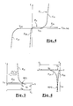
- Figure 4 shows the current / voltage curve F1 of the tunnel capacity Ct, which corresponds to the relation (1) mentioned above, and represents also the current / voltage curve F2 of the diode Dj.
- the curve F1 includes a half curve F11 for the voltages positive and a half curve F12 for the voltages negative.
- a current begins to cross the tunnel capacity Ct when the voltage Vc across its terminals is higher than a positive threshold voltage Vc1 or is lower than a negative threshold voltage Vc2.
- the curve F2 of the diode Dj comprises a half-curve F21 for positive voltages (curve conventional current / voltage of a polarized diode in inverse) and a half-curve F22 for the voltages negative (classic current / voltage curve of a diode polarized in the passing direction).
- a similar verification can be done by considering that a negative voltage V1 lower than Vc2 appears in the polysilicon line.
- the two half-curves F12 and F22 are transferred to the same graph, represented in figure 6, corresponding to Figure negative voltages and currents dial 4.
- the half-curves F11 and F21 have a common operating point WP2 where they cross, corresponding to a negative current Ic2, which guarantees the flow of loads electrostatic.
- the half-curve F12 disappears to the right of the dial and the current Ic2 decreases until it becomes zero.
- the combination of a contact antistatic according to the invention and an NP or PN junction ensures sufficient flow of loads electrostatic when the voltage V1 appearing in the polysilicon line exceeds a certain threshold Vc1, Vc2.
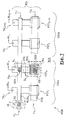
- Figure 7 illustrates an application of this invention for the protection of polysilicon lines present in erasable and programmable memories electrically.
- Figure 7 shows very schematically, from a top view, the topography of a word line WLi of rank i of a memory MEM electrically erasable and programmable.
- the word line WLi includes a plurality of gate transistors floating FGT1-FGTn, ... FGTj-FGT (j + n), ... arranged in columns COL1, ... COLk, ...
- Each column includes n FGT transistors and each FGT transistor includes a floating grid FG in polysilicon and a grid of CG control.
- the CG control grid extends above from the FG floating grid and is separated from it by a layer of GOX gate oxide.
- the floating grid FG extends over a BLK silicon substrate and is separated from it by a TOX tunnel oxide layer.
- GOX and TOX oxides are marked with lines hatched on the figure but are actually under the control grid CG and under the floating grid FG.
- the CG control grid is a section of a line of CGL grid control that passes over the grids floating points of all FGT transistors of the same column.
- Each FGT transistor is connected to a line of BL bit of corresponding rank (BL1-BLn ... BLj-BL (j + n) ...) via an access transistor TA (TA1-TAn ... TAj-TA (j + n)).
- the access transistor TA includes two doped regions D1, D2 forming drain and source, extending on either side of a GTA grid in polysilicon. Between the GTA grid and the BLK substrate is finds a GOX gate oxide.
- the GTA grids of TA access transistors belonging to the same word line WLi are connected to a common line WLSLi (line of word line selection).
- the WLSLi line is in polysilicon and passes between regions D1 and D2, where it forms the GTA gates of the access transistors TA.
- a such WLSLi line is relatively long to the other polysilicon lines because it crosses everything the memory plane horizontally to interconnect the GTA grids of the access transistors. She behaves as an "antenna" in the presence of electric charges and must be protected against the accumulation of charges can damage the GOX grid oxides of TA access transistors.
- an antistatic contact 21 at one end of the WLSLi line, an antistatic contact 21 according to the invention.
- This one includes the doped region 5 described above, implanted in the BLK substrate, and the thin oxide layer 22 extending under the line WLSLi.
- FIGS 8A to 8E are sectional views illustrating steps in a process for manufacturing a integrated circuit 50 including joint manufacturing an antistatic contact according to the invention and a floating gate transistor gate.
- Each figure has a left part and a right part corresponding to different cutting axes, for example an axis C1-C1 'shown in Figure 7 for the part left of each figure and a section axis C2-C2 'for the right part of each figure.
- the thicknesses of various layers of materials are not shown at scale for the sake of readability of these figures.
- regions A1, A2, A3 are first delimited on the surface of a substrate of silicon 30, here of type P, thanks to barriers isolation 31 performed using a standard process isolation (thick oxide, LOCOS, STI ).
- the regions N + doped 32-1, 32-2, 32-3 are then implanted in the substrate, respectively in each of the regions A1, A2, A3.
- Regions 32-2 and 32-3 are represented in dashed lines because they are not in the section plane (like for example the region D1 or D2 in figure 7).
- a gate oxide layer 33 is then formed on the entire substrate by growth of oxide. For the sake of clarity of the figure, the oxide 33 is found on isolation barriers 31 is not represented.
- openings 34-1 and 34-3 are practiced in the oxide layer 33, in regions A1 and A3, by etching the layer oxide.
- a tunnel oxide layer 35 is then formed over the entire substrate, by growth of oxide.
- the tunnel oxide layer 35 is typically of a thickness of the order of 0.002 to 0.015 micrometer depending on the manufacturing technology used and the voltage that the integrated circuit is intended for to receive.
- the gate oxide layer 33 is of a significantly greater thickness, generally around a few hundredths of a micrometer.
- tunnel oxide 35 formed on the isolation barriers 31 and on the gate oxide layer 33 is not shown, its thickness being negligible, only the tunnel oxide 35 formed at the bottom of the openings 34-1 and 34-3 being shown.
- a layer of polysilicon 36 is deposited on the entire substrate, then is engraved to reveal lines interconnection, MOS transistor grids and floating grids of FGT transistors.
- a line of polysilicon 36-1 is formed in the regions A1 and A2 and a floating grid 36-3 is formed in region A3.
- the polysilicon line 36-1 extends in opening 34-1 where it comes into contact with the oxide tunnel 35 extending above the substrate (doped region 32-1), the assembly thus forming an antistatic contact 21 according to the invention. So during the engraving of the polysilicon line 36-1 and later stages of manufacturing process, the polysilicon line 36-1 is protected against accumulation of charges electrostatic.
- a layer insulator 37 is formed on the entire substrate, by growth or deposition of ONO type oxide or insulator (Oxide-Nitride-Oxide).
- An opening 38 is then practiced in the insulating layer 37, above the polysilicon line 36-1, by etching layer 37.
- a layer of polysilicon 39 is deposited on the insulating layer 37, then is engraved to reveal lines interconnection and control grids FGT floating gate transistors.
- a control grid 39-3 is made above the floating grid 36-3 and a line 39-1 is produced above from line 36-1.
- Line 39-1 is in contact with line 36-1 thanks to the opening 38 made in the insulating layer 37, and is thus connected to the substrate via the antistatic contact 21, which also protects it against the accumulation of charges electrostatic.
- Lines 36-1 and 39-1 form by example a WLSLi word line selection line of the type described above (fig. 7).
- Line 36-1 forms also in region A2 and next to region doped 32-2, an access transistor gate TA.
- making a contact antistatic according to the invention does not include any step tunnel oxide removal and integrates perfectly in the manufacturing process of an integrated circuit, without requiring an additional processing step, being noted that the opening 34-1 in the oxide layer 33 is performed at the same time as opening 34-3 and others openings of the same type intended to receive the grids floating FGT transistors.
- the realization of a classic antistatic contact would require removal of the tunnel oxide 35 located at the bottom of the opening 34-1.
- a layer of polysilicon should first be deposited on the tunnel oxide. Layer of polysilicon should then be etched so that get next to opening 34-1 another opening forming etching mask of the tunnel oxide.
Landscapes
- Semiconductor Memories (AREA)
- Metal-Oxide And Bipolar Metal-Oxide Semiconductor Integrated Circuits (AREA)
- Non-Volatile Memory (AREA)
- Insulated Gate Type Field-Effect Transistor (AREA)
- Electrodes Of Semiconductors (AREA)
- Semiconductor Integrated Circuits (AREA)
Abstract
Description
- la figure 1 précédemment décrite est une vue en coupe partielle d'un circuit intégré comprenant un contact antistatique classique,
- la figure 2 est une vue en coupe partielle d'un circuit intégré comprenant un contact antistatique selon l'invention,
- la figure 3 est le schéma électrique de la combinaison d'un contact antistatique selon l'invention et d'une jonction NP,
- les figures 4, 5 et 6 représentent des courbes courant-tension qui illustrent les propriétés électriques d'un contact antistatique selon l'invention, et
- la figure 7 est une vue de dessus d'un circuit intégré comprenant un contact antistatique selon l'invention,
- les figures 8A à 8E illustrent des étapes d'un procédé de fabrication d'un circuit intégré selon l'invention.
Claims (9)
- Circuit intégré (20, 50) sur substrat de silicium (1, 30) comprenant au moins une ligne de polysilicium (4, 36-1, 39-1) reliant une pluralité de composants électroniques tels que des transistors MOS, et au moins un contact antistatique reliant la ligne de polysilicium au substrat de silicium, caractérisé en ce que le contact antistatique (21) comprend une couche d'oxyde fin (22, 35) agencée entre la ligne de polysilicium et le substrat de silicium, la couche d'oxyde fin étant d'une épaisseur suffisamment faible pour qu'un courant (Ic, Ic1, Ic2) la traverse par effet tunnel lorsque la ligne de polysilicium (4, 36-1, 39-1) est portée relativement au substrat à une tension (V1) supérieure ou inférieure à un seuil déterminé (Vc1, Vc2).
- Circuit intégré selon la revendication 1, dans lequel le contact antistatique est agencé au-dessus d'une région dopée (5, 32-1) formant avec le substrat une jonction NP ou PN.
- Circuit intégré selon l'une des revendications 1 et 2, dans laquelle la couche d'oxyde fin présente une épaisseur comprise entre 0,002 et 0,015 micromètre.
- Circuit intégré selon la revendication 3, comprenant au moins un transistor (FGT) à grille flottante (36-3) présentant une grille flottante (36-3) qui est isolée du substrat (30) par une couche d'oxyde tunnel (35) formant également la couche d'oxyde fin du contact antistatique.
- Circuit intégré selon l'une des revendications 1 à 4, formant une mémoire effaçable et programmable électriquement (MEM).
- Procédé de fabrication d'un circuit intégré (50) comprenant la fabrication d'une ligne de polysilicium reliant une pluralité de composants électroniques tels que des transistors MOS, et d'au moins un contact antistatique entre la ligne de polysilicium (36-1) et un substrat de silicium (30), comprenant les étapes consistant à :caractérisé en ce que la couche de polysilicium (36) est déposée sans retrait préalable de la deuxième couche d'oxyde (35) présente au fond de l'ouverture (34-1), et en ce que la deuxième couche d'oxyde (35) est d'une épaisseur suffisamment faible pour qu'un courant (Ic, Ic1, Ic2) la traverse par effet tunnel lorsque la ligne de polysilicium (36-1) est portée relativement au substrat à une tension (V1) supérieure ou inférieure à un seuil déterminé (Vc1, Vc2).faire croítre une première couche d'oxyde (33) sur le substrat de silicium (30),pratiquer au moins une ouverture (34-1) dans la première couche d'oxyde (33),faire croítre une deuxième couche d'oxyde (35) au fond de l'ouverture (34-1),déposer une couche de polysilicium (36) qui pénètre dans l'ouverture (34-1), etgraver la couche de polysilicium de manière à obtenir la ligne de polysilicium (36-1) et de manière que celle-ci s'étende au-dessus de l'ouverture (34-1),
- Procédé selon la revendication 6, comprenant une étape de gravure de la couche de polysilicium de manière à obtenir simultanément au moins la ligne de polysilicium (36-1) s'étendant au-dessus de l'ouverture (34-1) et au moins une grille flottante (36-3) d'un transistor à grille flottante, la grille flottante ne présentant pas de continuité électrique avec la ligne de polysilicium.
- Procédé selon l'une des revendications 6 et 7, comprenant une étape d'implantation de dopants dans le substrat, dans une région (32-1) se trouvant en regard de l'ouverture (34-1) pratiquée dans la première couche d'oxyde (33), pour former une jonction NP ou PN relativement au substrat.
- Procédé selon l'une des revendications 6 à 8, dans lequel le circuit intégré (50) est une mémoire effaçable et programmable électriquement (MEM).
Applications Claiming Priority (2)
| Application Number | Priority Date | Filing Date | Title |
|---|---|---|---|
| FR0108776A FR2826779A1 (fr) | 2001-07-02 | 2001-07-02 | Contact antistatique pour ligne en silicium polycristallin |
| FR0108776 | 2001-07-02 |
Publications (1)
| Publication Number | Publication Date |
|---|---|
| EP1274131A1 true EP1274131A1 (fr) | 2003-01-08 |
Family
ID=8865041
Family Applications (1)
| Application Number | Title | Priority Date | Filing Date |
|---|---|---|---|
| EP02012964A Withdrawn EP1274131A1 (fr) | 2001-07-02 | 2002-06-12 | Contact antistatique pour ligne en silicum polycristallin |
Country Status (4)
| Country | Link |
|---|---|
| US (1) | US20030001228A1 (fr) |
| EP (1) | EP1274131A1 (fr) |
| JP (1) | JP2003078052A (fr) |
| FR (1) | FR2826779A1 (fr) |
Families Citing this family (5)
| Publication number | Priority date | Publication date | Assignee | Title |
|---|---|---|---|---|
| US7160773B2 (en) * | 2004-05-05 | 2007-01-09 | Spansion Llc | Methods and apparatus for wordline protection in flash memory devices |
| JP2007194424A (ja) * | 2006-01-19 | 2007-08-02 | Matsushita Electric Ind Co Ltd | 保護素子およびその製造方法 |
| DE102006013209B4 (de) * | 2006-03-22 | 2017-03-09 | Austriamicrosystems Ag | Verfahren zur Herstellung von Halbleiterbauelementen mit Oxidschichten und Halbleiterbauelement mit Oxidschichten |
| US7745667B2 (en) * | 2008-04-07 | 2010-06-29 | Velocys | Microchannel apparatus comprising structured walls, chemical processes, methods of making formaldehyde |
| CN112180231B (zh) * | 2020-09-01 | 2021-09-14 | 长江存储科技有限责任公司 | 一种晶圆的失效分析方法 |
Citations (4)
| Publication number | Priority date | Publication date | Assignee | Title |
|---|---|---|---|---|
| EP0384275A2 (fr) * | 1989-02-21 | 1990-08-29 | National Semiconductor Corporation | Cellule mémoire MOS à profil de dopage exponentiel et ayant la région d'oxyde tunnel de la grille flottante décalée |
| JPH06283721A (ja) * | 1992-03-06 | 1994-10-07 | Oko Denshi Kofun Yugenkoshi | 不揮発性メモリ・セル、アレー装置、製造方法、及びそのメモリ回路 |
| JPH10200077A (ja) * | 1997-01-08 | 1998-07-31 | Sony Corp | 半導体装置及びその製造方法 |
| FR2786569A1 (fr) * | 1998-11-27 | 2000-06-02 | St Microelectronics Sa | Circuit de test de cellules eeprom |
-
2001
- 2001-07-02 FR FR0108776A patent/FR2826779A1/fr active Pending
-
2002
- 2002-06-07 US US10/165,051 patent/US20030001228A1/en not_active Abandoned
- 2002-06-12 EP EP02012964A patent/EP1274131A1/fr not_active Withdrawn
- 2002-06-27 JP JP2002188275A patent/JP2003078052A/ja active Pending
Patent Citations (4)
| Publication number | Priority date | Publication date | Assignee | Title |
|---|---|---|---|---|
| EP0384275A2 (fr) * | 1989-02-21 | 1990-08-29 | National Semiconductor Corporation | Cellule mémoire MOS à profil de dopage exponentiel et ayant la région d'oxyde tunnel de la grille flottante décalée |
| JPH06283721A (ja) * | 1992-03-06 | 1994-10-07 | Oko Denshi Kofun Yugenkoshi | 不揮発性メモリ・セル、アレー装置、製造方法、及びそのメモリ回路 |
| JPH10200077A (ja) * | 1997-01-08 | 1998-07-31 | Sony Corp | 半導体装置及びその製造方法 |
| FR2786569A1 (fr) * | 1998-11-27 | 2000-06-02 | St Microelectronics Sa | Circuit de test de cellules eeprom |
Non-Patent Citations (2)
| Title |
|---|
| PATENT ABSTRACTS OF JAPAN vol. 1998, no. 12 31 October 1998 (1998-10-31) * |
| PATENT ABSTRACTS OF JAPAN vol. 1999, no. 07 31 March 1999 (1999-03-31) * |
Also Published As
| Publication number | Publication date |
|---|---|
| US20030001228A1 (en) | 2003-01-02 |
| JP2003078052A (ja) | 2003-03-14 |
| FR2826779A1 (fr) | 2003-01-03 |
Similar Documents
| Publication | Publication Date | Title |
|---|---|---|
| EP0517607B1 (fr) | Procédé de fabrication d'une cellule de mémoire non volatile et cellule de mémoire obtenue | |
| EP2577730B1 (fr) | Circuit integre a dispositif de type fet sans jonction et a depletion | |
| EP2208201B1 (fr) | Cellule memoire sram dotee de transistors a structure multi-canaux verticale | |
| EP0648375B1 (fr) | Memoire eeprom de type flash a triples grilles et son procede de fabrication | |
| KR100866960B1 (ko) | 반도체 집적 회로 | |
| FR2911721A1 (fr) | Dispositif a mosfet sur soi | |
| EP1292984A1 (fr) | Memoire electronique a architecture damascene et procede de realisation d'une telle memoire | |
| FR2957457A1 (fr) | Procede de fabrication d'un point memoire anti-fusible | |
| EP0581625A1 (fr) | Composant életronique multifonctions, notamment élément à résistance dynamique négative, et procédé de fabrication correspondant | |
| EP0896370B1 (fr) | Dispositif de mémoire à grille flottante sur SOI et procédé de fabrication correspondant | |
| EP1274131A1 (fr) | Contact antistatique pour ligne en silicum polycristallin | |
| FR2996956A1 (fr) | Circuit integre comportant des transistors avec des tensions de seuil differentes | |
| US20030178664A1 (en) | Method of making non volatile memory with a protective metal line | |
| FR3093590A1 (fr) | Procédé de fabrication d’un élément capacitif, et circuit intégré correspondant. | |
| EP0379449A1 (fr) | Procédé de fabrication de circuits intégrés | |
| FR2995139A1 (fr) | Transistor mos | |
| EP1343208A1 (fr) | Mémoire non volatile programmable et effaçable électriquement à une seule couche de matériau de grille | |
| EP0626728B1 (fr) | Circuit integré du type à résistance, capacité et transistor, procédé de fabrication d'un tel circuit intégré et application à un oscillateur | |
| EP3404730B1 (fr) | Memoire non volatile favorisant une grande densite d'integration | |
| FR3122284A1 (fr) | Circuit intégré comportant au moins un élément capacitif et procédé de fabrication correspondant. | |
| EP0607075B1 (fr) | Composant électronique semi-conducteur à résistance dynamique négative, méthodes d'utilisation et procédé de fabrication correspondants | |
| EP0948038B1 (fr) | Procédé de fabrication d'une diode à avalanche à seuil réglable | |
| FR3109017A1 (fr) | PROCÉDÉ DE FABRICATION D’UNE PUCE À CIRCUIT INTÉGRÉ sur SeOI | |
| FR3160051A1 (fr) | Procédé de fabrication d’un dispositif électronique | |
| FR3069377A1 (fr) | Transistor mos a double blocs de grille a tension de claquage augmentee |
Legal Events
| Date | Code | Title | Description |
|---|---|---|---|
| PUAI | Public reference made under article 153(3) epc to a published international application that has entered the european phase |
Free format text: ORIGINAL CODE: 0009012 |
|
| AK | Designated contracting states |
Kind code of ref document: A1 Designated state(s): AT BE CH CY DE DK ES FI FR GB GR IE IT LI LU MC NL PT SE TR |
|
| AX | Request for extension of the european patent |
Free format text: AL;LT;LV;MK;RO;SI |
|
| RAP1 | Party data changed (applicant data changed or rights of an application transferred) |
Owner name: STMICROELECTRONICS SA |
|
| 17P | Request for examination filed |
Effective date: 20030611 |
|
| AKX | Designation fees paid |
Designated state(s): DE FR GB IT |
|
| 17Q | First examination report despatched |
Effective date: 20030922 |
|
| 17Q | First examination report despatched |
Effective date: 20030922 |
|
| STAA | Information on the status of an ep patent application or granted ep patent |
Free format text: STATUS: THE APPLICATION IS DEEMED TO BE WITHDRAWN |
|
| 18D | Application deemed to be withdrawn |
Effective date: 20070828 |