EP1274149A2 - Herstellungsverfahren für Hochfrequenzschaltung und Hochfrequenzschaltung - Google Patents
Herstellungsverfahren für Hochfrequenzschaltung und Hochfrequenzschaltung Download PDFInfo
- Publication number
- EP1274149A2 EP1274149A2 EP02012482A EP02012482A EP1274149A2 EP 1274149 A2 EP1274149 A2 EP 1274149A2 EP 02012482 A EP02012482 A EP 02012482A EP 02012482 A EP02012482 A EP 02012482A EP 1274149 A2 EP1274149 A2 EP 1274149A2
- Authority
- EP
- European Patent Office
- Prior art keywords
- radio frequency
- frequency circuit
- metal substrate
- circuit
- hollow bore
- Prior art date
- Legal status (The legal status is an assumption and is not a legal conclusion. Google has not performed a legal analysis and makes no representation as to the accuracy of the status listed.)
- Ceased
Links
Images




Classifications
-
- H—ELECTRICITY
- H05—ELECTRIC TECHNIQUES NOT OTHERWISE PROVIDED FOR
- H05K—PRINTED CIRCUITS; CASINGS OR CONSTRUCTIONAL DETAILS OF ELECTRIC APPARATUS; MANUFACTURE OF ASSEMBLAGES OF ELECTRICAL COMPONENTS
- H05K1/00—Printed circuits
- H05K1/18—Printed circuits structurally associated with non-printed electric components
-
- H—ELECTRICITY
- H10—SEMICONDUCTOR DEVICES; ELECTRIC SOLID-STATE DEVICES NOT OTHERWISE PROVIDED FOR
- H10W—GENERIC PACKAGES, INTERCONNECTIONS, CONNECTORS OR OTHER CONSTRUCTIONAL DETAILS OF DEVICES COVERED BY CLASS H10
- H10W44/00—Electrical arrangements for controlling or matching impedance
- H10W44/20—Electrical arrangements for controlling or matching impedance at high-frequency [HF] or radio frequency [RF]
-
- H—ELECTRICITY
- H01—ELECTRIC ELEMENTS
- H01P—WAVEGUIDES; RESONATORS, LINES, OR OTHER DEVICES OF THE WAVEGUIDE TYPE
- H01P11/00—Apparatus or processes specially adapted for manufacturing waveguides or resonators, lines, or other devices of the waveguide type
-
- H—ELECTRICITY
- H01—ELECTRIC ELEMENTS
- H01P—WAVEGUIDES; RESONATORS, LINES, OR OTHER DEVICES OF THE WAVEGUIDE TYPE
- H01P5/00—Coupling devices of the waveguide type
- H01P5/08—Coupling devices of the waveguide type for linking dissimilar lines or devices
- H01P5/10—Coupling devices of the waveguide type for linking dissimilar lines or devices for coupling balanced lines or devices with unbalanced lines or devices
- H01P5/107—Hollow-waveguide/strip-line transitions
-
- H—ELECTRICITY
- H05—ELECTRIC TECHNIQUES NOT OTHERWISE PROVIDED FOR
- H05K—PRINTED CIRCUITS; CASINGS OR CONSTRUCTIONAL DETAILS OF ELECTRIC APPARATUS; MANUFACTURE OF ASSEMBLAGES OF ELECTRICAL COMPONENTS
- H05K3/00—Apparatus or processes for manufacturing printed circuits
- H05K3/44—Manufacturing insulated metal core circuits or other insulated electrically conductive core circuits
-
- H—ELECTRICITY
- H05—ELECTRIC TECHNIQUES NOT OTHERWISE PROVIDED FOR
- H05K—PRINTED CIRCUITS; CASINGS OR CONSTRUCTIONAL DETAILS OF ELECTRIC APPARATUS; MANUFACTURE OF ASSEMBLAGES OF ELECTRICAL COMPONENTS
- H05K1/00—Printed circuits
- H05K1/02—Details
- H05K1/0213—Electrical arrangements not otherwise provided for
- H05K1/0216—Reduction of cross-talk, noise or electromagnetic interference
- H05K1/0218—Reduction of cross-talk, noise or electromagnetic interference by printed shielding conductors, ground planes or power plane
-
- H—ELECTRICITY
- H05—ELECTRIC TECHNIQUES NOT OTHERWISE PROVIDED FOR
- H05K—PRINTED CIRCUITS; CASINGS OR CONSTRUCTIONAL DETAILS OF ELECTRIC APPARATUS; MANUFACTURE OF ASSEMBLAGES OF ELECTRICAL COMPONENTS
- H05K1/00—Printed circuits
- H05K1/02—Details
- H05K1/0213—Electrical arrangements not otherwise provided for
- H05K1/0237—High frequency adaptations
-
- H—ELECTRICITY
- H05—ELECTRIC TECHNIQUES NOT OTHERWISE PROVIDED FOR
- H05K—PRINTED CIRCUITS; CASINGS OR CONSTRUCTIONAL DETAILS OF ELECTRIC APPARATUS; MANUFACTURE OF ASSEMBLAGES OF ELECTRICAL COMPONENTS
- H05K1/00—Printed circuits
- H05K1/02—Details
- H05K1/03—Use of materials for the substrate
- H05K1/05—Insulated conductive substrates, e.g. insulated metal substrate
- H05K1/056—Insulated conductive substrates, e.g. insulated metal substrate the metal substrate being covered by an organic insulating layer
-
- H—ELECTRICITY
- H05—ELECTRIC TECHNIQUES NOT OTHERWISE PROVIDED FOR
- H05K—PRINTED CIRCUITS; CASINGS OR CONSTRUCTIONAL DETAILS OF ELECTRIC APPARATUS; MANUFACTURE OF ASSEMBLAGES OF ELECTRICAL COMPONENTS
- H05K2201/00—Indexing scheme relating to printed circuits covered by H05K1/00
- H05K2201/03—Conductive materials
- H05K2201/0332—Structure of the conductor
- H05K2201/0364—Conductor shape
- H05K2201/037—Hollow conductors, i.e. conductors partially or completely surrounding a void, e.g. hollow waveguides
-
- H—ELECTRICITY
- H05—ELECTRIC TECHNIQUES NOT OTHERWISE PROVIDED FOR
- H05K—PRINTED CIRCUITS; CASINGS OR CONSTRUCTIONAL DETAILS OF ELECTRIC APPARATUS; MANUFACTURE OF ASSEMBLAGES OF ELECTRICAL COMPONENTS
- H05K2201/00—Indexing scheme relating to printed circuits covered by H05K1/00
- H05K2201/09—Shape and layout
- H05K2201/09209—Shape and layout details of conductors
- H05K2201/09654—Shape and layout details of conductors covering at least two types of conductors provided for in H05K2201/09218 - H05K2201/095
- H05K2201/0969—Apertured conductors
-
- H—ELECTRICITY
- H05—ELECTRIC TECHNIQUES NOT OTHERWISE PROVIDED FOR
- H05K—PRINTED CIRCUITS; CASINGS OR CONSTRUCTIONAL DETAILS OF ELECTRIC APPARATUS; MANUFACTURE OF ASSEMBLAGES OF ELECTRICAL COMPONENTS
- H05K2201/00—Indexing scheme relating to printed circuits covered by H05K1/00
- H05K2201/10—Details of components or other objects attached to or integrated in a printed circuit board
- H05K2201/10227—Other objects, e.g. metallic pieces
- H05K2201/10371—Shields or metal cases
-
- H—ELECTRICITY
- H05—ELECTRIC TECHNIQUES NOT OTHERWISE PROVIDED FOR
- H05K—PRINTED CIRCUITS; CASINGS OR CONSTRUCTIONAL DETAILS OF ELECTRIC APPARATUS; MANUFACTURE OF ASSEMBLAGES OF ELECTRICAL COMPONENTS
- H05K2203/00—Indexing scheme relating to apparatus or processes for manufacturing printed circuits covered by H05K3/00
- H05K2203/06—Lamination
- H05K2203/063—Lamination of preperforated insulating layer
-
- H—ELECTRICITY
- H05—ELECTRIC TECHNIQUES NOT OTHERWISE PROVIDED FOR
- H05K—PRINTED CIRCUITS; CASINGS OR CONSTRUCTIONAL DETAILS OF ELECTRIC APPARATUS; MANUFACTURE OF ASSEMBLAGES OF ELECTRICAL COMPONENTS
- H05K2203/00—Indexing scheme relating to apparatus or processes for manufacturing printed circuits covered by H05K3/00
- H05K2203/30—Details of processes not otherwise provided for in H05K2203/01 - H05K2203/17
- H05K2203/308—Sacrificial means, e.g. for temporarily filling a space for making a via or a cavity or for making rigid-flexible PCBs
-
- H—ELECTRICITY
- H05—ELECTRIC TECHNIQUES NOT OTHERWISE PROVIDED FOR
- H05K—PRINTED CIRCUITS; CASINGS OR CONSTRUCTIONAL DETAILS OF ELECTRIC APPARATUS; MANUFACTURE OF ASSEMBLAGES OF ELECTRICAL COMPONENTS
- H05K3/00—Apparatus or processes for manufacturing printed circuits
- H05K3/0058—Laminating printed circuit boards onto other substrates, e.g. metallic substrates
- H05K3/0061—Laminating printed circuit boards onto other substrates, e.g. metallic substrates onto a metallic substrate, e.g. a heat sink
-
- H—ELECTRICITY
- H10—SEMICONDUCTOR DEVICES; ELECTRIC SOLID-STATE DEVICES NOT OTHERWISE PROVIDED FOR
- H10W—GENERIC PACKAGES, INTERCONNECTIONS, CONNECTORS OR OTHER CONSTRUCTIONAL DETAILS OF DEVICES COVERED BY CLASS H10
- H10W44/00—Electrical arrangements for controlling or matching impedance
- H10W44/20—Electrical arrangements for controlling or matching impedance at high-frequency [HF] or radio frequency [RF]
- H10W44/203—Electrical connections
- H10W44/216—Waveguides, e.g. strip lines
-
- H—ELECTRICITY
- H10—SEMICONDUCTOR DEVICES; ELECTRIC SOLID-STATE DEVICES NOT OTHERWISE PROVIDED FOR
- H10W—GENERIC PACKAGES, INTERCONNECTIONS, CONNECTORS OR OTHER CONSTRUCTIONAL DETAILS OF DEVICES COVERED BY CLASS H10
- H10W70/00—Package substrates; Interposers; Redistribution layers [RDL]
- H10W70/60—Insulating or insulated package substrates; Interposers; Redistribution layers
- H10W70/62—Insulating or insulated package substrates; Interposers; Redistribution layers characterised by their interconnections
- H10W70/63—Vias, e.g. via plugs
-
- H—ELECTRICITY
- H10—SEMICONDUCTOR DEVICES; ELECTRIC SOLID-STATE DEVICES NOT OTHERWISE PROVIDED FOR
- H10W—GENERIC PACKAGES, INTERCONNECTIONS, CONNECTORS OR OTHER CONSTRUCTIONAL DETAILS OF DEVICES COVERED BY CLASS H10
- H10W70/00—Package substrates; Interposers; Redistribution layers [RDL]
- H10W70/60—Insulating or insulated package substrates; Interposers; Redistribution layers
- H10W70/67—Insulating or insulated package substrates; Interposers; Redistribution layers characterised by their insulating layers or insulating parts
- H10W70/68—Shapes or dispositions thereof
- H10W70/682—Shapes or dispositions thereof comprising holes having chips therein
-
- H—ELECTRICITY
- H10—SEMICONDUCTOR DEVICES; ELECTRIC SOLID-STATE DEVICES NOT OTHERWISE PROVIDED FOR
- H10W—GENERIC PACKAGES, INTERCONNECTIONS, CONNECTORS OR OTHER CONSTRUCTIONAL DETAILS OF DEVICES COVERED BY CLASS H10
- H10W70/00—Package substrates; Interposers; Redistribution layers [RDL]
- H10W70/60—Insulating or insulated package substrates; Interposers; Redistribution layers
- H10W70/67—Insulating or insulated package substrates; Interposers; Redistribution layers characterised by their insulating layers or insulating parts
- H10W70/68—Shapes or dispositions thereof
- H10W70/685—Shapes or dispositions thereof comprising multiple insulating layers
-
- H—ELECTRICITY
- H10—SEMICONDUCTOR DEVICES; ELECTRIC SOLID-STATE DEVICES NOT OTHERWISE PROVIDED FOR
- H10W—GENERIC PACKAGES, INTERCONNECTIONS, CONNECTORS OR OTHER CONSTRUCTIONAL DETAILS OF DEVICES COVERED BY CLASS H10
- H10W72/00—Interconnections or connectors in packages
- H10W72/071—Connecting or disconnecting
- H10W72/075—Connecting or disconnecting of bond wires
-
- H—ELECTRICITY
- H10—SEMICONDUCTOR DEVICES; ELECTRIC SOLID-STATE DEVICES NOT OTHERWISE PROVIDED FOR
- H10W—GENERIC PACKAGES, INTERCONNECTIONS, CONNECTORS OR OTHER CONSTRUCTIONAL DETAILS OF DEVICES COVERED BY CLASS H10
- H10W72/00—Interconnections or connectors in packages
- H10W72/50—Bond wires
- H10W72/541—Dispositions of bond wires
- H10W72/5445—Dispositions of bond wires being orthogonal to a side surface of the chip, e.g. parallel arrangements
-
- H—ELECTRICITY
- H10—SEMICONDUCTOR DEVICES; ELECTRIC SOLID-STATE DEVICES NOT OTHERWISE PROVIDED FOR
- H10W—GENERIC PACKAGES, INTERCONNECTIONS, CONNECTORS OR OTHER CONSTRUCTIONAL DETAILS OF DEVICES COVERED BY CLASS H10
- H10W72/00—Interconnections or connectors in packages
- H10W72/50—Bond wires
- H10W72/551—Materials of bond wires
-
- H—ELECTRICITY
- H10—SEMICONDUCTOR DEVICES; ELECTRIC SOLID-STATE DEVICES NOT OTHERWISE PROVIDED FOR
- H10W—GENERIC PACKAGES, INTERCONNECTIONS, CONNECTORS OR OTHER CONSTRUCTIONAL DETAILS OF DEVICES COVERED BY CLASS H10
- H10W72/00—Interconnections or connectors in packages
- H10W72/851—Dispositions of multiple connectors or interconnections
- H10W72/874—On different surfaces
- H10W72/884—Die-attach connectors and bond wires
-
- H—ELECTRICITY
- H10—SEMICONDUCTOR DEVICES; ELECTRIC SOLID-STATE DEVICES NOT OTHERWISE PROVIDED FOR
- H10W—GENERIC PACKAGES, INTERCONNECTIONS, CONNECTORS OR OTHER CONSTRUCTIONAL DETAILS OF DEVICES COVERED BY CLASS H10
- H10W72/00—Interconnections or connectors in packages
- H10W72/90—Bond pads, in general
- H10W72/951—Materials of bond pads
-
- H—ELECTRICITY
- H10—SEMICONDUCTOR DEVICES; ELECTRIC SOLID-STATE DEVICES NOT OTHERWISE PROVIDED FOR
- H10W—GENERIC PACKAGES, INTERCONNECTIONS, CONNECTORS OR OTHER CONSTRUCTIONAL DETAILS OF DEVICES COVERED BY CLASS H10
- H10W90/00—Package configurations
- H10W90/701—Package configurations characterised by the relative positions of pads or connectors relative to package parts
- H10W90/731—Package configurations characterised by the relative positions of pads or connectors relative to package parts of die-attach connectors
- H10W90/734—Package configurations characterised by the relative positions of pads or connectors relative to package parts of die-attach connectors between a chip and a stacked insulating package substrate, interposer or RDL
-
- H—ELECTRICITY
- H10—SEMICONDUCTOR DEVICES; ELECTRIC SOLID-STATE DEVICES NOT OTHERWISE PROVIDED FOR
- H10W—GENERIC PACKAGES, INTERCONNECTIONS, CONNECTORS OR OTHER CONSTRUCTIONAL DETAILS OF DEVICES COVERED BY CLASS H10
- H10W90/00—Package configurations
- H10W90/701—Package configurations characterised by the relative positions of pads or connectors relative to package parts
- H10W90/731—Package configurations characterised by the relative positions of pads or connectors relative to package parts of die-attach connectors
- H10W90/736—Package configurations characterised by the relative positions of pads or connectors relative to package parts of die-attach connectors between a chip and a stacked lead frame, conducting package substrate or heat sink
-
- H—ELECTRICITY
- H10—SEMICONDUCTOR DEVICES; ELECTRIC SOLID-STATE DEVICES NOT OTHERWISE PROVIDED FOR
- H10W—GENERIC PACKAGES, INTERCONNECTIONS, CONNECTORS OR OTHER CONSTRUCTIONAL DETAILS OF DEVICES COVERED BY CLASS H10
- H10W90/00—Package configurations
- H10W90/701—Package configurations characterised by the relative positions of pads or connectors relative to package parts
- H10W90/751—Package configurations characterised by the relative positions of pads or connectors relative to package parts of bond wires
- H10W90/754—Package configurations characterised by the relative positions of pads or connectors relative to package parts of bond wires between a chip and a stacked insulating package substrate, interposer or RDL
-
- Y—GENERAL TAGGING OF NEW TECHNOLOGICAL DEVELOPMENTS; GENERAL TAGGING OF CROSS-SECTIONAL TECHNOLOGIES SPANNING OVER SEVERAL SECTIONS OF THE IPC; TECHNICAL SUBJECTS COVERED BY FORMER USPC CROSS-REFERENCE ART COLLECTIONS [XRACs] AND DIGESTS
- Y10—TECHNICAL SUBJECTS COVERED BY FORMER USPC
- Y10T—TECHNICAL SUBJECTS COVERED BY FORMER US CLASSIFICATION
- Y10T156/00—Adhesive bonding and miscellaneous chemical manufacture
- Y10T156/10—Methods of surface bonding and/or assembly therefor
- Y10T156/1052—Methods of surface bonding and/or assembly therefor with cutting, punching, tearing or severing
Definitions
- the present invention relates to a radio frequency circuit manufactured by using a metal-core substrate having an insulating material laminated on a metal substrate such as of copper or aluminum or the like and, more particularly, to a manufacturing method for a radio frequency circuit on a high frequency range of a microwave or millimeter-wave band and to such a radio frequency circuit.
- the metal-core substrate having an insulating material laminated on a metal substrate such as of copper or aluminum, known as a radio frequency circuit substrate, is marketed under the product name of Diacore by Mitsubishi Resin.
- the radio frequency circuit manufactured by the use of such a metal-core substrate allows heat dissipation from the metal substrate.
- a radio frequency circuit can be manufactured having high heat dissipation characteristic.
- the copper or aluminum uses a thickness of nearly 100 ⁇ m or greater, generally approximately 500 ⁇ m-3 mm, from the relationship of connection with a housing accommodating the radio frequency circuit.
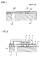
- Fig. 1 shows an example of a radio frequency circuit utilizing a metal-core substrate.
- This radio frequency circuit is structured with an insulating material 102 having a low dielectric loss formed on a metal substrate 101, such as of copper or aluminum, a transmission line 103 formed on the insulating material 102, and a through-hole 104 formed with a conductor to electrically, thermally conductively connect between the metal substrate 101 and the transmission line 103.
- the insulating material 102 is selected with a material having a low dielectric loss (low dielectric loss tangent) characteristic, such as polyimide or teflon, in order to reduce the dielectric loss over the transmission line.
- a material having a low dielectric loss (low dielectric loss tangent) characteristic such as polyimide or teflon
- a hollow bore 105 is formed in the metal substrate 101. Meanwhile, it is possible to connect a waveguide transmitting a signal inputted from an antenna to the hollow bore 105, thereby structuring a converter for converting a membrane-structured circuit portion from the waveguide into a planar circuit.
- the metal substrate 101 it is a general practice to form a mask on the substrate 101 to carry out etching thereby forming a hollow bore 105.
- a mask it is difficult to form a hollow bore 105 into a desired form. Namely, the hollow bore 105 would be isotropic in form and etched to a somewhat inward of a mask.
- the metal substrate 101 has a thickness of 1 mm, it requires a working time of 3 hour and 20 minutes provided that the etching rate on the metal substrate 101 is 5 ⁇ m/min. Thus, the method cannot be considered an efficient working method.
- a hollow bore 105 is previously provided in a metal substrate 101 to hot-press an insulating material 102.
- the insulating material 102 flows in the hollow bore 105 of the metal substrate 101 thereby making it difficult to obtain a favorable membrane structure.
- the present invention has been made in view of the foregoing point, and it is an object to provide a method capable of easily manufacturing a radio frequency circuit of a membrane structure type.
- a manufacturing method for a radio frequency circuit of the present invention is a method for manufacturing a radio frequency circuit comprising: a first step of forming a circuit by using an insulating material having metal, such as copper, bonded on both surfaces or one surface; a second step of bonding together a metal substrate having a hollow bore and the circuit made in the first step; a third step of mounting an active element on the circuit; and a fourth step of connecting the circuit made in the third step with a lid having a partition wall.
- the partition wall provided on the lid is formed in an outer periphery of the lid to surround the radio frequency circuit.
- the interior of the lid is filled with vacuum, an inert gas or a nitrogen gas, as required.
- the metal substrate is formed with a convex projection having a hollow bore at an inside thereof, as required.
- the insulating material preferably, has a dielectric loss tangent value of 0.003 or smaller at 1 GHz.
- Another method for manufacturing a radio frequency circuit of the invention comprises: a first step of blanking a metal substrate with a die to form a hollow bore; a second step of carrying out a surface treatment or cleaning with a plasma or ozone on a metal small plate blanked by a die; a third step of inserting the surface-treated metal small plate into the hollow bore of the metal substrate; and a fourth step of placing an insulating material forming a circuit onto the metal substrate and thereafter hot-press it for bonding.
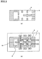
- Fig. 2 shows an example of a radio frequency circuit fabricated by using a manufacturing method for a radio frequency circuit according to the present invention.
- a metal substrate 1 is of copper, copper-containing alloy or aluminum having a thickness of 100 ⁇ m or greater, generally 500 ⁇ m or greater, on which an insulating plate 2 is formed.
- the insulating plate 2 is formed of an insulating material having a low dielectric loss (dielectric loss of nearly 0.05 or less).
- the insulating plate 2 preferably has, as a material characteristic, a dielectric loss tangent value of approximately 0.003 or less at a measuring frequency of 1 GHz.
- a glass-epoxy-based insulating material called FR-4 a general circuit-substrate insulation material, has a dielectric loss tangent of approximately 0.02 at a measuring frequency of 1 GHz. This is not preferred as an insulating material for fabricating a high-frequency circuit on a microwave or millimeter-wave band.
- the insulating plate 2 is selected of a material having a low dielectric loss characteristic (low dielectric loss tangent) such as polyimide, teflon, liquid-crystal polymer or benzocyclo butene, in order to reduce the dielectric loss over a transmission line.
- a material having a low dielectric loss characteristic such as polyimide, teflon, liquid-crystal polymer or benzocyclo butene
- the insulating plate 2 has transmission lines 3, such as micro-strip lines, coplanar-strip lines, slot lines or ground lines, formed on the both surface thereof. Meanwhile, the insulating plate 2 is formed with hollow bores buried by a conductor. Thus, through-holes 4 are formed to connect between the transmission lines 3 on the opposite surfaces of the insulating plate 2 in an electrical, thermal conductive fashion.
- the metal substrate 1 has a hollow bore 5 serving as a waveguide to provide a membrane structure.
- the transmission line 3, on the upper surface of the insulating plate 2 has a high-frequency circuit pattern to arrange, thereon, active elements 6 such as MMICs (millimeter-wave (or microwave) monolithic integrated circuits), HBTs (hetero-junction bipolar transistors) or HEMTs (high electron mobility transistors).
- active elements 6 such as MMICs (millimeter-wave (or microwave) monolithic integrated circuits), HBTs (hetero-junction bipolar transistors) or HEMTs (high electron mobility transistors).
- the active element 6 and the transmission line 3 are connected through a wire 7, to constitute a desired high-frequency circuit.
- a lid 8, covering over the high-frequency circuit for the purpose of electromagnetic shield, is bonded on the transmission line 3 on the upper surface of the insulating plate 2.
- the portion of the transmission line 3 extending outside the lid 8 provides a connection terminal to an external device.
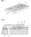
- Fig. 3A is a plan view of the radio frequency circuit shown in Fig. 2 when removed of the lid 8, as viewing the radio frequency circuit from the below.
- Fig. 3B is a plan view of the radio frequency circuit removed of the lid 8, as viewed from the above.
- the hatched area shows the transmission line 3 of Fig. 2 while the dotted line 5 shows that the hollow bore 5 formed in the metal plate 1 of Fig. 2 exists in a region below the insulating plate 2.
- the hollow bore 5 as a waveguide, the slot line 19 and the lid 8 constitute a waveguide-planar line converting circuit.
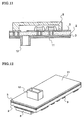
- the lid 8 of Fig. 3A is shown, as a perspective view, in Fig. 4.
- the hatched area, in Figs. 3A and 4 is an area to be directly contacted with the radio frequency circuit of Fig. 3B.
- This area structures a partition wall 9 corresponding to the transmission line 3 and active element 6.
- the partition wall 9 particularly serves to suppress against the unwanted radio wave released from the active element 6. Besides the prevention of emission of unwanted radio wave toward an outside of the radio frequency circuit, it is possible to prevent the mutual interference of radio waves between the active elements 6. Thus, reliability can be improved for the entire radio frequency circuit.
- the reliability can be further improved for the radio frequency circuit.
- Fig. 5A shows a process for manufacturing a circuit substrate by forming transmission lines 3 on the both surfaces of a low-loss insulating plate 2 and through-holes 4 formed with a conductor for electrically, thermal conductively connecting between the transmission lines 3 on the both surfaces.
- the insulating plate 2 and the transmission lines 3 use a sheet-formed material marketed called a lamination plate bonded with copper at both surfaces. This is opened by penetration holes in positions corresponding to through-holes 4 by drilling, laser or etching, and buried by a connection conductor in the penetration holes, thereby forming through-holes 4.
- Fig. 5B shows a process for bonding a circuit substrate fabricated by the process of Fig. 5A onto a metal substrate 1 previously formed with a hollow bore 5.
- the method for forming a hollow bore 5 in the metal substrate 1 may use machining with the use of milling or press-blanking. The method using press-blanking is most effective in respect of working efficiency.
- the method for bonding the circuit substrate made in the process of Fig. 5A and the metal substrate 1 together may use a bonding process using an adhesive or bonding agent high in electrical or thermal conductivity. Otherwise, these may be bonded directly or through a thermo-plastic or thermo-set film having electrical or thermal conductivity by the application of heat and pressure.
- Fig. 5C shows a process for electrically connecting an active element 6 onto the transmission line 3 by a wire-bonding technique.
- the electrical connection between the active element 6 and the transmission line 3 may use a flip-chip mounting scheme instead of the wire-bonding technique.
- Fig. 5D shows a process for bonding the lid 8 onto the circuit substrate.
- the bonding may be by a similar method to the foregoing bonding of between the circuit substrate and the metal substrate 1, the effective bonding method, above all, is to apply a paste epoxy-based adhesive agent to the partition wall 9, a hatched area, of the lid 8 shown in Fig. 4 by the use of a dispenser and then thermally cure it after bonding.
- Embodiment 1 can fabricate, by a simple way, a membrane-structured radio frequency circuit in a precise form posed as a problem in using a metal core substrate. Also, the efficiency can be enhanced in fabricating a radio frequency circuit.
- the radio frequency circuit made by the manufacturing method can be used in a radio terminal, base-station apparatus, radio measuring apparatus, radar apparatus or the like. Thus, a reliable apparatus is to be obtained.
- Fig. 6 shows an example of a sectional structure of a radio frequency circuit according to Embodiment 2 of the invention.
- the radio frequency circuit of Embodiment 2 is an example that a transmission line 3 is grounded to a metal substrate 1 by through-holes 4.
- the difference from the radio frequency circuit shown in Fig. 2 lies in that no transmission line 3 exists between the metal substrate 1 and the insulating plate 2.
- the manufacturing method is similar to that of Embodiment 1 excepting that a lamination plate bonded with copper at one surface is used in place of a lamination plate bonded with copper at both surfaces explained in Fig. 5A, and hence omittedly explained.
- Fig. 7 shows an example of a sectional structure of a radio frequency circuit according to Embodiment 3 of the invention.
- the active element 6 is bonded on the transmission line 3 through a conductive adhesive agent 18.
- An antenna 10 inputs and outputs a radio wave to and from an outside of the apparatus.
- the region A in the figure coupled to the antenna 10 constitutes a waveguide-planar line converter.
- the region A is in a form having a dielectric material 2 above a hollow bore 5. This structure is generally called a membrane structure.
- the transmission line 3 is electrically connected to a metal substrate 1 as a conductor through a through-hole 4.
- the metal substrate 1 serves as a ground of the transmission line 3. Meanwhile, the heat generated by the active element 6 diffuses through the through-hole 4 to the metal substrate 1.
- the metal substrate 1 serves as a dissipater of heat to the outside, thus having a function to cool down a microwave or millimeter-wave device including the waveguide-plane line converter.
- Fig. 8 shows an example of a sectional structure of a radio frequency circuit according to Embodiment 4 of the invention.
- This is a circuit nearly equivalent to the circuit shown in Fig. 2 but different from Fig. 2 in that the region shown at B, or active element 6, is directly contacted with a transmission line 3 of beneath an insulating material 2.
- the radio frequency circuit of a structure shown in Fig. 8 can structure a radio frequency circuit having a high heat dissipation effect because the heat generated from the active element 6 is allowed to dissipate directly at the transmission line 3 or through the metal substrate 1.
- the manufacturing method for this radio frequency circuit is similar to the manufacturing method explained in Embodiment 1 excepting that a hollow bore for an active element 6 is provided in place of the through-hole 4 in the process of Fig. 5A and an active element 6 is provided in the hollow bore in the process of Fig. 5C.
- Embodiment 4 it is possible to fabricate, by a simple way, a precise-formed membrane-structured radio frequency circuit excellent in heat dissipation characteristic.
- Fig. 9 shows an example of a sectional structure of a radio frequency circuit according to Embodiment 5 of the invention. This is a circuit nearly equivalent to the circuit shown in Fig. 2 but different from Fig. 2 in a part shown at C.
- Fig. 9 is different from Fig. 2 in that insulating materials 21, 22 are in a two-layer form, transmission lines 301, 302, 303 are in a three-layer form and a partition wall 9 formed on the lid 8 has a peripheral form extending over the entire periphery of the lid 8 as in a perspective view of Fig. 10.
- an internal transmission line 3 covered by the lid 8 is extended to a transmission line 303 outside the lid 8 through a through-hole 41, a transmission line 302 on a lower insulating material 22 and a through-hole 42, thus being extended to the outside without contact with the lid 8. Consequently, the lid 8 at its entire periphery can be provided as a surface to be directly bonded to the radio frequency circuit.
- an inert gas such as argon (Ar) or nitrogen (N 2 ) therein, the radio frequency circuit is shielded from the outside air. This can prevent the active elements 6 from deteriorating due to aging by the reaction with oxygen or humidity of the air.
- the circuit manufacturing method shown in Figs. 5A - 5D is to be applied without change.
- Embodiment 5 it is possible to provide a reliable, precise-formed radio frequency circuit of a membrane structure.
- Fig. 11 shows an example of a sectional structure of a radio frequency circuit according to Embodiment 6 of the invention.
- This is a circuit nearly equivalent to the circuit shown in Fig. 2 but different in that a convex part 12 is formed in a metal substrate 11 in a membrane region of a radio frequency circuit.
- Fig. 12 is a perspective view of Fig. 11 as viewed from a bottom side.
- the manufacturing method for a metal substrate 11 having a convex part 12 although to be achieved by machining with cutting or etching, can use deep drawing by using press with excellence in respect of material use efficiency and operation time efficiency.
- the radio frequency circuit manufacture in the other process is similar to that of Figs. 5A - 5D.
- the radio frequency circuit structured with the metal substrate 11 shown in Figs. 11 and 12 is in a structure convenient for connection to another radio frequency circuit device.
- Fig. 13 is a view showing an example of a form that the radio frequency circuit shown in Fig. 11 is connected with another radio frequency circuit.
- the radio frequency circuit to be connected comprises an antenna 13 and a connection housing 14 built with a waveguide region 15.
- the connection housing 14 is connected to the metal substrate 11 such that a convex part 12 of the metal substrate 11 is coupled to a waveguide 15 of the housing 14. This allows the metal substrate 11 to operate as a part of a waveguide for a radio wave 16 to be inputted or outputted at the antenna 13.
- the circuit in a membrane structure, for a radio wave 16 transmitted and received at the antenna 13 serves as a waveguide-planar circuit converting device that converts the waveguide 15 into a planar circuit structured by an insulating material 2, a transmission line 3, a through-hole 4, an active element and a lid 8.
- Embodiment 6 facilitates the connection with another radio frequency element part as shown in the example of Fig. 13, thus achieving size-reduction in the entire circuit.
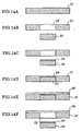
- Figs. 14A - 14F show a part of a process of a radio frequency circuit manufacturing method for manufacturing a microwave or millimeter-wave device including a waveguide-planar line converter. This shows a process for manufacturing a membrane structure bonding a metal substrate and a dielectric material together.
- Fig. 14A is a state having only a metal substrate 21.
- a blanking penetration hole 22 is formed in the metal plate 21 by pressing using a die.
- Fig. 14C shows a state that a blanked metal small plate 23 is surface-treated at its upper surface to form a surface-treated layer 24.
- the surface-treated layer 24 is formed by applying a silicon-based or teflon-based surface treating material, or coating or evaporating an organic film of polyimide or the like.
- the surface treatment is for the purpose of making the metal small plate 23 having the surface-treatment layer 24 less bondable to a dielectric material during bonding between the dielectric material and the metal substrate in the later process.
- FIG. 14D shows a process of inserting the metal small plate 23 formed with the surface-treatment layer 24 into the penetration hole 22 of the metal substrate 21.
- Fig. 14E shows a process of hot-pressing a dielectric material 25 and bonding it onto the metal substrate 21. At this time, because of the presence of the metal small plate 23, the dielectric material 25 can be formed without flowing into the penetration hole 22 existing in the metal substrate 21.
- the dielectric material 25 used in this process be reduced in dielectric loss because the invention is applied for a high frequency range of a microwave or millimeter-wave band.
- a material having a property of low dielectric loss such as polyimide, teflon, polymer of polyimide and teflon, liquid-crystal polymer or benzocyclo butene.
- Fig. 14F is a process of taking the metal small plate 23 having the surface-treatment layer 24 out of the metal substrate 21.
- the metal small plate 23, because of surface-treated, can be easily removed from the metal substrate 21 without being bonded to the dielectric material 25.
- a dielectric material 25 is formed on the metal substrate 21 having the penetration hole 22. This makes it possible to manufacture a favorably shaped membrane structure and hence a small-sized, high-function microwave or millimeter-wave device.
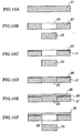
- Figs. 15A - 15F show a second method for manufacturing a membrane structure by bonding together a metal substrate 21 and a dielectric material 25.
- Figs. 15A and 15B are a process similar to that of Figs. 14A and 14B but different from Fig. 14 in the subsequent process.
- Fig. 15C is a process to carry out a plasma cleaning process or ozone cleaning process on a surface of the metal substrate 21.
- a treatment layer 26 is formed on the surface of the metal substrate 21 by the plasma cleaning or ozone cleaning process.
- the present inventor has found that, by carrying out a plasma cleaning or ozone cleaning process prior to hot-pressing the metal substrate 21 and dielectric material 25, the adhesion force between the metal substrate 21 and the dielectric material 25 after hot-pressing is to be by far improved. Furthermore, it has been confirmed that, by carrying out a plasma cleaning or ozone cleaning process also on a bonding surface of the dielectric material 25 to the metal substrate 21, the adhesion force can be improved furthermore. By utilizing this nature to carry out a plasma cleaning or ozone cleaning process only on the metal substrate 21 having the penetration hole 22 without surface-treating the metal small plate 23, it is possible to facilitate the separation of the metal small plate 22 from the metal substrate 21 in the process of Fig. 15F.
- the plasma cleaning methods include an atmospheric pressure plasma scheme for directly radiating a plasma in the air, a parallel-plate plasma etching scheme for plasma processing in a vacuum, and a reactive ion etching scheme.
- the reactive plasma etching scheme is the highest in cleaning effect.
- the cleaning condition in using a reactive plasma etching scheme includes, as an example, a mixing ration of O 2 gas and CF 4 gas of 4 : 1, a gas total flow rate of 50 sccm, a vacuum degree of 20 Pa, an RF power (13.56 MHz) of 1.2 W/cm 2 , and a plasma radiation time of 30 seconds. Under this condition, the adhesion force was secured between the metal substrate 21 and the dielectric material 25 in Fig. 15E. It can be considered that the reason of adhesion force improvement is because of the following. Namely, the pollutant of carbon or the like deposited on a surface of the metal substrate 21 due to exposure to the air could be removed away by the plasma.
- an inductive coupling plasma etching scheme or the like may be used besides the reactive plasma etching scheme.
- the cleaning using ozone refers to a method that, after placing a metal substrate and dielectric material to be cleaned within a container filled with O 2 gas, ultraviolet light is radiated to the O 2 gas to ozonize the O 2 gas and thereby activate it so that it is reacted with the deposit, such as carbon, on the metal substrate and dielectric material thereby removing the same.
- Fig. 15D and the subsequent are a process nearly the same as that of Fig. 14D and the subsequent.
- Fig. 15D shows a process of returning the metal small plate 23 to the metal substrate 21, Fig. 15E a process of bonding the metal substrate 21 and the dielectric material 25 together by hot-press, and
- Fig. 15F a process of taking out the metal small plate 23.
- the metal substrate 21 is not done with a plasma cleaning or ozone cleaning process and hence can be easily separated without bonding to the dielectric material 25.
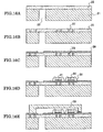
- Fig. 16A - 16E are a process view of a manufacturing method for a radio frequency circuit according to Embodiment 9 of the invention.
- Fig. 16A is a membrane structure manufactured by the method of Embodiment 7 or 8.
- Fig. 16B shows a process of forming a penetration hole 27 for a through-hole in a dielectric material 25.
- the forming method for a penetration hole 27 preferably uses the laser working having a laser oscillation wavelength of ultraviolet light. This is because a through-hole diameter of 0.03 mm or smaller is difficult to realize by drilling.
- dry etching has an etching rate of approximately 0.5 - 2 ⁇ m/min so that, when a dielectric material is 100 ⁇ m, it takes a working time of 50 - 200 minutes and mask forming process is further required. Accordingly, these are not to be considered as a practical forming method.
- laser working it is possible to carry out working by the use of a general carbon dioxide gas laser.
- the working using a carbon dioxide gas laser, as thermal working has a defect to form a thermal deterioration layer in the dielectric film.
- the laser working method having a laser oscillation wavelength of ultraviolet light such as in an excimer or YAG laser third harmonic, because ablation of a dielectric material is predominant in a working mechanism, it is possible to suppress thermal damage to the dielectric material.
- Fig. 16C shows a process for forming a transmission line 28 including conductor formation in the penetration hole 27.
- the transmission line formation can be made by combining plating, metal film sputtering, resist forming/exposure/development, conductive paste forming and the like.
- the conductor formed in the penetration hole 27 forms a through-hole 29.
- Fig. 16D shows a process of mounting an active element 30, such as a MMIC, HBT or HEMT. After forming a conductive adhesive 31 on the transmission line 28 (electrically not connected to another transmission line), an active element 30 is mounted thereon. The conductive adhesive 31 is hardened by thermal cure or the like. Electrical connection is made through a wire 32 to another transmission line 28.
- an active element 30 such as a MMIC, HBT or HEMT.
- a lid 33 as a shield is bonded by using a conductive paste, as shown in Fig. 16E.
- Fig. 17A - 17E is a radio frequency circuit manufacturing method similar in process to that shown in Fig. 16A - 16E but different in that an active element 30 is mounted directly on a metal substrate 21.
- Fig. 17A is the same as Fig. 16A, which is in a membrane structure manufactured by the method of Embodiment 7 or 8.
- Fig. 17B shows a process of forming, in a dielectric material 25, a penetration hole 27 for a through-hole and a space 35 for mounting an active element 30.
- the forming method for a penetration hole 27 and space 35 preferably uses the laser working having a laser oscillation wavelength of ultraviolet light because of the reason explained in Embodiment 9.
- Fig. 17C is a process of forming a transmission line 28 by the same method as Fig. 16C.
- Fig. 17D is a process of mounting an active element 30 directly on the metal substrate 21. The mounting method is the same as that of Fig. 16D.
- the heat generated by the active element 30 can be directly released to the metal substrate 21 having high thermal diffusibility.
- This provides a reliable microwave or millimeter-wave device.
- the wire 32 can be substantially shortened, e.g. where the dielectric material 25 has a thickness of 100 ⁇ m and the active element 30 also has a thickness of 100 ⁇ m. By shortening the wire 32 length, circuit impedance modulation can be suppressed thereby making possible to manufacture a high-quality microwave or millimeter-wave device.
- the metal substrate 1, 11, 21 if using a material of copper or copper-containing alloy is effective in respect of environmental consideration. This is because copper can be readily recovered by the use of copper chloride or iron chloride. In recent years, electronic appliance recycling has being sought to push forward.
- the use of easily recoverable copper as a metal substrate can enhance the ability of recycling the microwave or millimeter-wave device including waveguide-planar line converter and the communication terminal, base-station apparatus, radio measuring apparatus and radar apparatus using the same device.
Landscapes
- Engineering & Computer Science (AREA)
- Manufacturing & Machinery (AREA)
- Microelectronics & Electronic Packaging (AREA)
- Waveguides (AREA)
Applications Claiming Priority (4)
| Application Number | Priority Date | Filing Date | Title |
|---|---|---|---|
| JP2001204331 | 2001-07-05 | ||
| JP2001204331 | 2001-07-05 | ||
| JP2002103297 | 2002-04-05 | ||
| JP2002103297A JP2003086728A (ja) | 2001-07-05 | 2002-04-05 | 高周波回路の製作方法及びそれを用いた装置 |
Publications (2)
| Publication Number | Publication Date |
|---|---|
| EP1274149A2 true EP1274149A2 (de) | 2003-01-08 |
| EP1274149A3 EP1274149A3 (de) | 2003-10-01 |
Family
ID=26618178
Family Applications (1)
| Application Number | Title | Priority Date | Filing Date |
|---|---|---|---|
| EP02012482A Ceased EP1274149A3 (de) | 2001-07-05 | 2002-06-12 | Herstellungsverfahren für Hochfrequenzschaltung und Hochfrequenzschaltung |
Country Status (6)
| Country | Link |
|---|---|
| US (1) | US20030024633A1 (de) |
| EP (1) | EP1274149A3 (de) |
| JP (1) | JP2003086728A (de) |
| KR (1) | KR20030005024A (de) |
| CN (1) | CN1462088A (de) |
| TW (1) | TW543118B (de) |
Cited By (12)
| Publication number | Priority date | Publication date | Assignee | Title |
|---|---|---|---|---|
| US7248222B2 (en) | 2005-03-15 | 2007-07-24 | Fujitsu Limited | High-frequency module |
| EP1923950A1 (de) | 2006-11-17 | 2008-05-21 | Siemens S.p.A. | SMT-fähiges Mikrowellenbauteil mit Wellenleiterschnittstelle |
| WO2008128808A1 (de) * | 2007-04-23 | 2008-10-30 | Continental Automotive Gmbh | Modul für eine integrierte steuerelektronik mit vereinfachtem aufbau |
| WO2009045667A1 (en) * | 2007-10-03 | 2009-04-09 | The Boeing Company | Advanced antenna integrated printed wiring board with metallic waveguide plate |
| EP1937040A3 (de) * | 2006-12-22 | 2009-07-01 | Siemens Aktiengesellschaft | Leiterplatte mit einem Hochfrequenzbauelement |
| EP2110884A1 (de) * | 2008-04-15 | 2009-10-21 | Huber+Suhner Ag | Flächenmontierbare Antenne mit Wellenleiter-Anschlussfunktion, Kommunikationssystem, Adapter und Anordnung mit der Antennenvorrichtung |
| EP1983614A4 (de) * | 2006-02-06 | 2010-01-06 | Mitsubishi Electric Corp | Hochfrequenzmodul |
| EP1729340A4 (de) * | 2004-03-26 | 2010-10-20 | Mitsubishi Electric Corp | Hochfrequenzgehäuse, sende- und empfangsmodul und drahtloses gerät |
| EP2043150A3 (de) * | 2007-09-28 | 2011-11-02 | Delphi Technologies, Inc. | Mikrowellenkommunikationspaket |
| EP2618421A1 (de) * | 2012-01-19 | 2013-07-24 | Huawei Technologies Co., Ltd. | Oberflächenmontiertes Mikrowellensystem |
| GB2502908B (en) * | 2011-01-21 | 2015-04-08 | Ibm | Antenna with a waveguide feed structure suitable for IC chip package applications |
| WO2019166064A1 (de) * | 2018-03-01 | 2019-09-06 | Conti Temic Microelectronic Gmbh | Radarsystem zur umfelderfassung eines kraftfahrzeugs mit einer kunststoffantenne |
Families Citing this family (26)
| Publication number | Priority date | Publication date | Assignee | Title |
|---|---|---|---|---|
| JP2004071670A (ja) * | 2002-08-02 | 2004-03-04 | Fuji Photo Film Co Ltd | Icパッケージ、接続構造、および電子機器 |
| JP4064403B2 (ja) * | 2005-01-18 | 2008-03-19 | シャープ株式会社 | 半導体装置、表示モジュール、半導体チップ実装用フィルム基板の製造方法、及び半導体装置の製造方法 |
| JP2006253953A (ja) * | 2005-03-09 | 2006-09-21 | Fujitsu Ltd | 通信用高周波モジュールおよびその製造方法 |
| JP4503476B2 (ja) * | 2005-03-29 | 2010-07-14 | 株式会社ホンダエレシス | 高周波線路−導波管変換器 |
| WO2007091329A1 (ja) * | 2006-02-10 | 2007-08-16 | Fujitsu Limited | 電子部品パッケージ |
| JP4912716B2 (ja) * | 2006-03-29 | 2012-04-11 | 新光電気工業株式会社 | 配線基板の製造方法、及び半導体装置の製造方法 |
| CN101578697B (zh) * | 2007-03-14 | 2011-12-28 | 三菱电机株式会社 | 高频封装件 |
| JP2009160988A (ja) * | 2007-12-28 | 2009-07-23 | Omron Corp | 検出装置および方法、並びに、プログラム |
| EP2159558A1 (de) * | 2008-08-28 | 2010-03-03 | Sensirion AG | Verfahren zur Herstellung eines integrierten Drucksensors |
| US9941242B2 (en) | 2012-04-24 | 2018-04-10 | Innogration (Suzhou) Co., Ltd. | Unpacked structure for power device of radio frequency power amplification module and assembly method therefor |
| CN102623416B (zh) | 2012-04-24 | 2015-09-02 | 苏州远创达科技有限公司 | 一种射频功放模块的功率器件无封装结构及其组装方法 |
| JP6095444B2 (ja) | 2013-03-29 | 2017-03-15 | 富士通テン株式会社 | アンテナ装置およびレーダ装置 |
| CN203279336U (zh) * | 2013-04-27 | 2013-11-06 | 中兴通讯股份有限公司 | 一种内散热的终端 |
| JP6372113B2 (ja) * | 2014-03-17 | 2018-08-15 | 富士通株式会社 | 高周波モジュール及びその製造方法 |
| JP6520281B2 (ja) * | 2015-03-24 | 2019-05-29 | 富士通株式会社 | 電子機器筐体 |
| CN108141959B (zh) * | 2015-10-06 | 2020-02-07 | 住友电工印刷电路株式会社 | 印刷线路板和电子部件 |
| CN105555018A (zh) * | 2016-02-16 | 2016-05-04 | 广东欧珀移动通信有限公司 | 一种印刷电路板及电子终端 |
| US10325850B1 (en) * | 2016-10-20 | 2019-06-18 | Macom Technology Solutions Holdings, Inc. | Ground pattern for solderability and radio-frequency properties in millimeter-wave packages |
| TWI659518B (zh) * | 2017-05-18 | 2019-05-11 | Siliconware Precision Industries Co., Ltd. | 電子封裝件及其製法 |
| CN107546181B (zh) * | 2017-08-18 | 2019-07-05 | 华进半导体封装先导技术研发中心有限公司 | 雷达组件封装体 |
| CN107479034B (zh) * | 2017-08-18 | 2019-10-18 | 华进半导体封装先导技术研发中心有限公司 | 雷达组件封装体及其制造方法 |
| CN107548244B (zh) * | 2017-08-30 | 2020-02-28 | 景旺电子科技(龙川)有限公司 | 一种双面夹芯铜基板内部铜基之间绝缘的制作方法 |
| CN110010485A (zh) * | 2018-10-10 | 2019-07-12 | 浙江集迈科微电子有限公司 | 一种具有光路转换功能的密闭型光电模块制作工艺 |
| CN109786985B (zh) * | 2018-12-12 | 2024-09-20 | 南京安捷智造科技有限公司 | 一种基于接地共面波导的矩形微带串馈天线 |
| US12022608B2 (en) * | 2021-03-11 | 2024-06-25 | Northrop Grumman Systems Corporation | Radio frequency crossover with high isolation in microelectronics H-frame device |
| DE102023205139A1 (de) | 2023-06-01 | 2024-12-05 | Robert Bosch Gesellschaft mit beschränkter Haftung | Leiterplatte mit einem Hohlwellenleiterkanal |
Family Cites Families (8)
| Publication number | Priority date | Publication date | Assignee | Title |
|---|---|---|---|---|
| GB1512605A (en) * | 1976-08-05 | 1978-06-01 | Standard Telephones Cables Ltd | Microwave integrated printed circuits |
| DE3129425A1 (de) * | 1981-07-25 | 1983-02-10 | Richard Hirschmann Radiotechnisches Werk, 7300 Esslingen | Mikrowellenantenne fuer zirkularpolarisation |
| GB2139818B (en) * | 1983-05-12 | 1986-10-22 | Marconi Electronic Devices | High frequency transmission device |
| JPS6271301A (ja) * | 1985-09-25 | 1987-04-02 | Matsushita Electric Ind Co Ltd | マイクロ波集積回路装置 |
| TW300345B (de) * | 1995-02-06 | 1997-03-11 | Matsushita Electric Industrial Co Ltd | |
| DE19805911A1 (de) * | 1998-02-13 | 1999-08-19 | Cit Alcatel | Übergang von einer Mikrostripleitung zu einem Hohlleiter sowie Verwendung eines solchen Übergangs |
| WO2001018901A1 (en) * | 1999-09-02 | 2001-03-15 | Commonwealth Scientific And Industrial Research Organisation | Feed structure for electromagnetic waveguides |
| JP2001230606A (ja) * | 2000-02-15 | 2001-08-24 | Matsushita Electric Ind Co Ltd | マイクロストリップ線路と、これを用いたマイクロ波装置 |
-
2002
- 2002-04-05 JP JP2002103297A patent/JP2003086728A/ja active Pending
- 2002-05-23 TW TW091110940A patent/TW543118B/zh not_active IP Right Cessation
- 2002-06-12 EP EP02012482A patent/EP1274149A3/de not_active Ceased
- 2002-07-02 US US10/187,735 patent/US20030024633A1/en not_active Abandoned
- 2002-07-04 KR KR1020020038543A patent/KR20030005024A/ko not_active Withdrawn
- 2002-07-05 CN CN02140614A patent/CN1462088A/zh active Pending
Cited By (17)
| Publication number | Priority date | Publication date | Assignee | Title |
|---|---|---|---|---|
| EP1729340A4 (de) * | 2004-03-26 | 2010-10-20 | Mitsubishi Electric Corp | Hochfrequenzgehäuse, sende- und empfangsmodul und drahtloses gerät |
| US7248222B2 (en) | 2005-03-15 | 2007-07-24 | Fujitsu Limited | High-frequency module |
| EP1983614A4 (de) * | 2006-02-06 | 2010-01-06 | Mitsubishi Electric Corp | Hochfrequenzmodul |
| US8040286B2 (en) | 2006-02-06 | 2011-10-18 | Mitsubishi Electric Corporation | High frequency module |
| EP1923950A1 (de) | 2006-11-17 | 2008-05-21 | Siemens S.p.A. | SMT-fähiges Mikrowellenbauteil mit Wellenleiterschnittstelle |
| EP1937040A3 (de) * | 2006-12-22 | 2009-07-01 | Siemens Aktiengesellschaft | Leiterplatte mit einem Hochfrequenzbauelement |
| WO2008128808A1 (de) * | 2007-04-23 | 2008-10-30 | Continental Automotive Gmbh | Modul für eine integrierte steuerelektronik mit vereinfachtem aufbau |
| EP2043150A3 (de) * | 2007-09-28 | 2011-11-02 | Delphi Technologies, Inc. | Mikrowellenkommunikationspaket |
| US7579997B2 (en) | 2007-10-03 | 2009-08-25 | The Boeing Company | Advanced antenna integrated printed wiring board with metallic waveguide plate |
| WO2009045667A1 (en) * | 2007-10-03 | 2009-04-09 | The Boeing Company | Advanced antenna integrated printed wiring board with metallic waveguide plate |
| EP2110884A1 (de) * | 2008-04-15 | 2009-10-21 | Huber+Suhner Ag | Flächenmontierbare Antenne mit Wellenleiter-Anschlussfunktion, Kommunikationssystem, Adapter und Anordnung mit der Antennenvorrichtung |
| WO2009127497A1 (en) * | 2008-04-15 | 2009-10-22 | Huber+Suhner Ag | Surface-mountable antenna with waveguide connector function, communication system, adaptor and arrangement comprising the antenna device |
| GB2502908B (en) * | 2011-01-21 | 2015-04-08 | Ibm | Antenna with a waveguide feed structure suitable for IC chip package applications |
| EP2618421A1 (de) * | 2012-01-19 | 2013-07-24 | Huawei Technologies Co., Ltd. | Oberflächenmontiertes Mikrowellensystem |
| US9647313B2 (en) | 2012-01-19 | 2017-05-09 | Huawei Technologies Co., Ltd. | Surface mount microwave system including a transition between a multilayer arrangement and a hollow waveguide |
| WO2019166064A1 (de) * | 2018-03-01 | 2019-09-06 | Conti Temic Microelectronic Gmbh | Radarsystem zur umfelderfassung eines kraftfahrzeugs mit einer kunststoffantenne |
| US11604273B2 (en) | 2018-03-01 | 2023-03-14 | Conti Temic Microelectronic Gmbh | Radar system for detecting the environment of a motor vehicle having a plastic antenna |
Also Published As
| Publication number | Publication date |
|---|---|
| CN1462088A (zh) | 2003-12-17 |
| EP1274149A3 (de) | 2003-10-01 |
| JP2003086728A (ja) | 2003-03-20 |
| US20030024633A1 (en) | 2003-02-06 |
| KR20030005024A (ko) | 2003-01-15 |
| TW543118B (en) | 2003-07-21 |
Similar Documents
| Publication | Publication Date | Title |
|---|---|---|
| US20030024633A1 (en) | Radio frequency circuit manufacturing method and radio frequency circuit | |
| US6849936B1 (en) | System and method for using film deposition techniques to provide an antenna within an integrated circuit package | |
| US6770822B2 (en) | High frequency device packages and methods | |
| US7445968B2 (en) | Methods for integrated circuit module packaging and integrated circuit module packages | |
| US7911292B2 (en) | Mode transition between a planar line and a waveguide with a low loss RF substrate and a high loss low frequency substrate | |
| US20060276157A1 (en) | Apparatus and methods for packaging antennas with integrated circuit chips for millimeter wave applications | |
| US20200083591A1 (en) | Semiconductor device package and method of manufacturing the same | |
| US8362608B2 (en) | Ultra wideband hermetically sealed surface mount technology for microwave monolithic integrated circuit package | |
| US20250233301A1 (en) | Antenna in package having antenna on package substrate | |
| CN107479034B (zh) | 雷达组件封装体及其制造方法 | |
| JP3209183B2 (ja) | 高周波信号用集積回路パッケージ及びその製造方法 | |
| CN114068436A (zh) | 封装电路结构及其制作方法 | |
| US20240178163A1 (en) | Slot Bow-Tie Antenna On Package | |
| US11784625B2 (en) | Packaging method and package structure for filter chip | |
| Nawaz et al. | Organically packaged components and modules: Recent advancements for microwave and mm-wave applications | |
| TWI651020B (zh) | 微電子系統、微電子設備及製造其之方法 | |
| US20230352850A1 (en) | Microelectronic device package with integral slotted waveguide antenna | |
| JP2003332517A (ja) | マイクロ波集積回路及びその製造方法並びに無線装置 | |
| JP4448461B2 (ja) | 半導体パッケージの作製方法 | |
| WO2019033608A1 (zh) | 雷达组件封装体及其制造方法 | |
| CN112038779A (zh) | 天线半导体封装装置及其制造方法 | |
| JP2005340713A (ja) | マルチチップモジュール | |
| US20240021971A1 (en) | Microelectronic device package with integral waveguide transition | |
| JP2001267487A (ja) | 高周波モジュール | |
| JP2001257234A (ja) | 半導体装置及びその製造方法 |
Legal Events
| Date | Code | Title | Description |
|---|---|---|---|
| PUAI | Public reference made under article 153(3) epc to a published international application that has entered the european phase |
Free format text: ORIGINAL CODE: 0009012 |
|
| AK | Designated contracting states |
Kind code of ref document: A2 Designated state(s): AT BE CH CY DE DK ES FI FR GB GR IE IT LI LU MC NL PT SE TR |
|
| AX | Request for extension of the european patent |
Free format text: AL;LT;LV;MK;RO;SI |
|
| PUAL | Search report despatched |
Free format text: ORIGINAL CODE: 0009013 |
|
| AK | Designated contracting states |
Kind code of ref document: A3 Designated state(s): AT BE CH CY DE DK ES FI FR GB GR IE IT LI LU MC NL PT SE TR |
|
| AX | Request for extension of the european patent |
Extension state: AL LT LV MK RO SI |
|
| 17P | Request for examination filed |
Effective date: 20031120 |
|
| 17Q | First examination report despatched |
Effective date: 20031223 |
|
| AKX | Designation fees paid |
Designated state(s): DE FR GB |
|
| STAA | Information on the status of an ep patent application or granted ep patent |
Free format text: STATUS: THE APPLICATION HAS BEEN REFUSED |
|
| 18R | Application refused |
Effective date: 20050130 |