EP2618421A1 - Oberflächenmontiertes Mikrowellensystem - Google Patents
Oberflächenmontiertes Mikrowellensystem Download PDFInfo
- Publication number
- EP2618421A1 EP2618421A1 EP12151801.3A EP12151801A EP2618421A1 EP 2618421 A1 EP2618421 A1 EP 2618421A1 EP 12151801 A EP12151801 A EP 12151801A EP 2618421 A1 EP2618421 A1 EP 2618421A1
- Authority
- EP
- European Patent Office
- Prior art keywords
- conductive layer
- microwave
- surface mount
- waveguide
- layer
- Prior art date
- Legal status (The legal status is an assumption and is not a legal conclusion. Google has not performed a legal analysis and makes no representation as to the accuracy of the status listed.)
- Ceased
Links
Images


Classifications
-
- H—ELECTRICITY
- H01—ELECTRIC ELEMENTS
- H01P—WAVEGUIDES; RESONATORS, LINES, OR OTHER DEVICES OF THE WAVEGUIDE TYPE
- H01P5/00—Coupling devices of the waveguide type
- H01P5/08—Coupling devices of the waveguide type for linking dissimilar lines or devices
- H01P5/10—Coupling devices of the waveguide type for linking dissimilar lines or devices for coupling balanced lines or devices with unbalanced lines or devices
- H01P5/107—Hollow-waveguide/strip-line transitions
-
- H—ELECTRICITY
- H01—ELECTRIC ELEMENTS
- H01P—WAVEGUIDES; RESONATORS, LINES, OR OTHER DEVICES OF THE WAVEGUIDE TYPE
- H01P3/00—Waveguides; Transmission lines of the waveguide type
- H01P3/02—Waveguides; Transmission lines of the waveguide type with two longitudinal conductors
- H01P3/08—Microstrips; Strip lines
- H01P3/081—Microstriplines
-
- H—ELECTRICITY
- H01—ELECTRIC ELEMENTS
- H01P—WAVEGUIDES; RESONATORS, LINES, OR OTHER DEVICES OF THE WAVEGUIDE TYPE
- H01P3/00—Waveguides; Transmission lines of the waveguide type
- H01P3/12—Hollow waveguides
- H01P3/121—Hollow waveguides integrated in a substrate
-
- H—ELECTRICITY
- H01—ELECTRIC ELEMENTS
- H01Q—ANTENNAS, i.e. RADIO AERIALS
- H01Q9/00—Electrically-short antennas having dimensions not more than twice the operating wavelength and consisting of conductive active radiating elements
- H01Q9/04—Resonant antennas
- H01Q9/0407—Substantially flat resonant element parallel to ground plane, e.g. patch antenna
-
- H—ELECTRICITY
- H10—SEMICONDUCTOR DEVICES; ELECTRIC SOLID-STATE DEVICES NOT OTHERWISE PROVIDED FOR
- H10W—GENERIC PACKAGES, INTERCONNECTIONS, CONNECTORS OR OTHER CONSTRUCTIONAL DETAILS OF DEVICES COVERED BY CLASS H10
- H10W90/00—Package configurations
- H10W90/701—Package configurations characterised by the relative positions of pads or connectors relative to package parts
- H10W90/751—Package configurations characterised by the relative positions of pads or connectors relative to package parts of bond wires
- H10W90/754—Package configurations characterised by the relative positions of pads or connectors relative to package parts of bond wires between a chip and a stacked insulating package substrate, interposer or RDL
Definitions
- the present invention relates to surface mount microwave systems.
- SMMS Surface mount microwave systems
- SoP system on package
- the SoPs may be provided with covers having embedded waveguide reflectors, as is described in the document EP 1 923 950 A1 . Therefore, such covers form a part of an electrical design which is associated with further electrical constraints which may be taken into account when designing the electrical characteristics of a SoP.
- the invention is based on the finding that an efficient surface mount microwave system may be provided if a number of electrical constraints limiting the electrical design is reduced. Such reduction may be achieved by a dedicated microwave transition structure for electromagnetically coupling e.g. a microstrip line of the surface mount microwave system with a hollow microwave waveguide. Such microwave transition structure may be arranged on the die of the surface mount microwave system. Therefore, a cover with a waveguide reflector is not necessary.
- a surface mount microwave system comprises a multilayer arrangement comprising a first conductive layer, a second conductive layer and a dielectric layer, wherein the first conductive layer is arranged on the dielectric layer, and wherein the dielectric layer is arranged on the second conductive layer, wherein the first conductive layer comprises a microwave circuit and wherein the second conductive layer forms a reference potential layer.
- a hollow microwave waveguide is at least partly formed in the second conductive layer, and a microwave transition structure for electromagnetically coupling the first conductive layer with the hollow microwave waveguide is provided.
- the microwave transition structure can for example be a part of the multilayer arrangement and provide a dedicated electromagnetical coupling between the first conductive layer and the hollow microwave waveguide.
- the microwave circuit in the surface mount microwave system at least a part of the first conductive layer forms or connects to the microwave circuit.
- the microwave circuit can for example be formed by conductive portions being shaped to have certain microwave characteristics.
- the microwave circuit can also be any electronic circuit, e.g. a MMIC.
- the microwave transition structure comprises a conductive microstrip radiating pattern being formed on the dielectric layer for irradiating an electromagnetic wave towards the hollow microwave waveguide.
- the microwave transition structure can for example be formed as a conductive structure by at least a part of the first conductive layer.
- the microstrip radiating pattern comprises a microstrip line being formed by the first conductive layer, and another microstrip line, the other microstrip line being wider than the microstrip line, the other microstrip line being attached to the broadened portion, the broadened portion being formed for irradiating an electromagnetic wave towards the hollow microwave waveguide.
- the broadened portion can for example form a radiating structure of pattern which enables an electromagnetical coupling towards the hollow microwave waveguide.
- the surface mount microwave system comprises a dielectric waveguide, which can for example be formed by a part of the dielectric layer.
- the dielectric waveguide is formed by a portion of the dielectric layer arranged between the first and second conductive layer.
- the portion of the dielectric layer can for example be arranged beneath the aforementioned broadened portion for a direct electromagnetical coupling.
- the portion of the dielectric layer can for example be surrounded or delimited by a plurality of grounded holes.
- the dielectric waveguide is formed by a portion of the dielectric layer arranged between the first and second conductive layer.
- the portion of the dielectric layer can for example be delimited by a grounded metalized slot surrounding the aforementioned broadened portion.
- the second conductive layer comprises a hollow portion, in particular a slot, forming at least a part of the hollow microwave waveguide.
- the second conductive layer can for example form walls of the hollow microwave waveguide.
- the second conductive layer comprises a hollow portion, in particular a slot, forming at least a part of the hollow microwave waveguide.
- the waveguide adaptor can for example form a radiating interface for interfacing towards the hollow microwave waveguide which can for example be formed by a slot in the second conductive layer.
- the second conductive layer has a thickness which is equal to or greater than 50% or 60% or 70% or 80% or 90% of a total thickness of the base stack.
- the first conductive layer, the dielectric layer and the second conductive layer form a dual layer laminate structure.
- the surface mount microwave system further comprises a third conductive layer forming a connecting layer which can for example be attached to the second layer by a FR4 prepreg.
- the surface mount microwave system further comprises a coaxial transmission line coupled or embedded on the second conductive layer e.g. for electrically connecting one or a plurality of pads on the third conductive layer to the first conductive layer.
- the surface mount microwave system further comprises one or a plurality of holes for connecting the ground portion of third layer to the reference potential layer.
- the second conductive layer forms a ground layer.
- the surface mount microwave system further comprises a further hollow waveguide having metallic walls formed by angular portions behind the second conductive layer forming a waveguide interface towards the hollow waveguide.
- the first conductive layer is hollowed down up to the second conductive layer to obtain at least one pocket for accommodating one or more microwave devices.
- the surface mount microwave system further comprises an attachable cover, e.g. a FR4 cover, with an outside metal plating, in particular an attachable cover for covering the first conductive layer and the attached microwave components.
- an attachable cover e.g. a FR4 cover
- an outside metal plating in particular an attachable cover for covering the first conductive layer and the attached microwave components.
- the attachable cover is be free of any electrical constraint and does not form any part of the microwave transition structure.
- the invention provides a package structure suitable up to 90GHz with the surface mount microwave system.
- the package structure comprises a microstrip to dielectric waveguide transition on the first conductive layer.
- a dielectric to air waveguide transition on the back side of the package is provided.
- a reflector is missing on the attachable cover.
- the attachable cover is externally metalized for shielding action only.
- the attachable cover exhibits, internally, high loss cavity preventing on air signal propagation.
- three layers compact PCB forms the multilayer arrangement.
- an inner thick copper plate is integral part of the microwave laminate forming the multilayer arrangement.
- an inner thick copper plate is an integral part of the waveguide transition design.
- the inner thick copper plate is an integral part of the high performance top-to-back coaxial connections.
- Fig. 1 shows a surface mount microwave system according to an implementation form.
- the surface mount microwave system comprises a multilayer arrangement 101 having a first conductive layer 103, a second conductive layer 105 and a dielectric layer 107.
- the first conductive layer 103 is at least partly arranged on the dielectric layer 107, wherein the dielectric layer 107 is arranged on the second conductive layer 105.
- the first conductive layer 103 comprises a microwave circuit 109, which is formed by a conductive pattern of the first conductive layer 103.
- the multilayer arrangement 101 can for example form a laminate structure with laminated layers according to an implementation form.
- the surface mount microwave system further comprises a hollow microwave waveguide 111 which is formed at least partly in the second conductive layer 105. Furthermore, a microwave transition structure 113 is provided for electromagnetically coupling the first conductive layer 103 and the hollow microwave waveguide 111.
- the surface mount microwave system further comprises a third conductive layer 114 for connecting to the first layer 103.
- the first conductive layer can for example comprise pads for connecting to any of the layers of the surface mount microwave system.
- the third conductive layer 114 can for example comprise a pad 115 connected via a via 117 to the second conductive layer 105.
- the third conductive layer 114 can for example further comprise a further pad 119 connected via another via 121 to the first conductive layer 103.
- the first conductive layer 103 can for example have a layer portion 109 connected via a via 125 to the second conductive layer 105.
- the surface mount microwave system further comprises an FR4 prepreg 126 arranged between the second conductive layer 105 and the third conductive layer 114.
- the surface mount microwave system comprises a further waveguide 127 having angular portions 129 and forming a waveguide interface towards the hollow microwave waveguide 111.
- the first connecting layer 103 can for example comprise copper (Cu) and may have a thickness of 0.017 mm.
- the dielectric layer 107 may have a thickness of 0.1 mm.
- the second conductive layer 105 may have a thickness of 0.7 mm and may comprise or consist of copper (Cu).
- the FR4 prepreg 126 can for example have a thickness of 0.1 mm, and the third conductive layer 114 may have a thickness of 0.017 mm.
- the FR4 prepreg 126 allows adding the third conductive layer 114 to obtain three conductive layers microwave printed circuit board.
- the first conductive layer 103 is used for microwave design
- the second conductive layer 105 is used for ground and power dissipation
- the first conductive layer 114 is used for connecting parts.
- the second conductive layer 105 has a thickness which may be 80% of the total height of a resulting printed circuit board which allows designing high performance top-to-back microwave coaxial connections.
- the third conductive layer 114 provides for proper SMT pads to interface the system with e.g. an external board for DC and RF connections and for signaling e.g. up to 29 GHZ.
- holes may be drilled through the multilayer arrangement comprising e.g. a copper foil forming the first conductive layer 103, a dielectric substrate forming the dielectric layer 107 and the copper baking forming the second conductive layer 107.
- the holes are filled with ceramic via hole filler. Thereafter, a grind flat are provided. Thereafter, through holes are drilled through the ceramic filler and blind grounding holes are provided. Thereafter, an aperture A is milled. Thereafter, a through hole and blind hole plate are provided. Thereafter, the via holes are filled with ceramic via hole filler. Thereafter, a grind are provided. Thereafter, over-plate vias and surface vias are provided. Thereafter, a tracking pattern on both sides may is printed and etched. Thereafter, milling the slot S is performed.
- the above-mentioned manufacturing steps may be different according to the PCB shop manufacturing process.
- a clean room surface mounted microwave system assembling process can for example be performed.
- the process comprises an epoxy dispensing, MMICs picking and placing, manual and/or visual inspection, curing (polymerization), plasma-cleaning, wire or ribbon bondings, DC test and cover attached by using e.g. a conductive glue.
- Fig. 2 shows a multilayer arrangement 201 according to an implementation form.
- the multilayer arrangement 201 differs from the multilayer arrangement 101 shown in Fig. 1 in that a hollow waveguide 203 with diameter or aperture S which is formed in the second conductive layer 105 has a broadened portion 205 with diameter or aperture A for interfacing purposes. Furthermore, blind ground holes 207 and a through isolated hole 209 are provided.
- Fig. 3 shows a back view on the surface mount microwave system as depicted in Fig. 1 according to an implementation form.
- the third conductive layer 114 i.e. the connecting layer, can for example comprise a plurality of signaling pads 301, e.g. DC (direct current) signaling parts.
- radio frequency (RF) microwave pads 303 may be provided.
- the microwave pads 303 may be surrounded by grounding holes 305 connecting to the second conductive layer 105 which is not depicted in Fig. 3 .
- a ground plane 307 is provided.
- the ground plane 307 is connected to the second conductive layer 105 via grounding holes 309.
- the ground plane 307 has a waveguide transition recess 311.
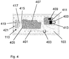
- Fig. 4 shows a top view of the surface mount microwave system as depicted in Fig. 1 according to an implementation form.
- the first conductive layer 103 may comprise a plurality of microwave circuits, e.g. microstrip lines 401 which for example are be surrounded by grounding holes 403.
- further microwave circuits 405 and 407 or other arrangements may be provided.
- the further microwave circuits 405, 407 or arrangements may respectively comprise a capacitor 409, a pocket 411, an MMIC 413 and further circuits.
- the microwave transition structure 101 comprises for example a microstrip line 415 and another microstrip line 417 forming a microstrip adapter.
- the packages shown in Figs. 3 and 4 can for example be 20 to 25 mm long and 10 to 15 mm wide.
- the dielectric waveguide 419 can for example be surrounded by ground holes 421.
- the surface mount microwave system can for example be provided with an attachable cover as e.g. shown in Figs. 5a, 5b and 5c .
- the attachable cover 501 as shown in Fig. 5a consist of copper and comprises angular portions 503.
- the attachable cover 501 defines a first space 505 accommodating at least a part of the surface mount microwave system.
- the attachable cover 501 may further define a proper thickness 507 providing mechanical robustness.
- Figs. 5a, 5b and 5c show different views of an attachable cover 501.
- the attachable cover 501 can for example have a plain structure.
- the cover 501 comprises or consist for example of 1.6 mm FR4 which is copper-plated outside and hollowed out internally for e.g. one half of its height as depicted in Fig. 5 .
- FR4 allows for preventing oscillations forming the dissipation factor which may attenuate an on-air signal propagation inside the package.
- the cover 501 is free of any electrical constraints.
- Fig. 6 shows an assembled package comprising the surface mount microwave system as depicted in Fig. 1 and the attachable cover 501 as depicted in Fig. 5 . Furthermore, a MMIC 413 can for example be provided.
- Fig. 7 shows a physical structure of a microwave transition structure 701 according to an implementation form.
- the microwave transition structure 701 can for example comprise a conductive microstrip radiating pattern which is formed on the dielectric layer 107.
- the microwave transition structure 701 comprises a microstrip line 703 and another microstrip line 705 which is wider than the microstrip line 703.
- the broadened portion 707 is arranged on a dielectric waveguide 709 which is formed by a part of the dielectric layer 107.
- the dielectric waveguide 709 connects to a slot 711 in the second conductive layer 105 which is not depicted in Fig. 7 for the fake of descriptional simplicity.
- the slot 711 i.e. the hollow microwave waveguide
- the other waveguide 715 can for example be a hollow microwave waveguide.
- the microwave transition structure e.g. the microwave transition structure 701
- forms a dielectric air waveguide transition which provides an input/output radiating interface backside the surface mount microwave system.
- a coaxial transmission line for connection is provided on the second conductive layer 105 for electrical connection.
- Figs. 8a and 8b respectively show a physical structure of a top-to-back coaxial connection 801 being formed on the second conductive layer 105 for operating in the frequency range between e.g. 20 to 35 GHz.
- a microstrip line 803 can for example be provided.
- the surface mount microwave system is deployed to provide MMICs which can for example be embodied into a SMT package, wherein more than one chip can for example be assembled into one package o obtain a multifunction system on package comprising e.g. a transmitter, a receiver or parts of them. Furthermore, according to some implementation forms, only a chip and via assembling line are used. Furthermore, according to some implementation forms, high-frequency bare dies are mounted inside the package so that a standard SMT automatic process is possible. According to some implementation forms, a low thermal resistance, e.g. smaller than 1°/ W, may be achieved which allows a dissipation up to few watt inside the package.
- a milling the PBC backside to obtain a waveguide radiating interface can for example be performed, so that a reflector on the cover is avoided. Therefore, the cover does not need to be electrically designed in a special way. Furthermore, the manufacturing process is PCB-based and does not need to be based on a metal insert structure. In addition, an open module operating capability can for example be provided.
Landscapes
- Waveguides (AREA)
- Waveguide Connection Structure (AREA)
Priority Applications (3)
| Application Number | Priority Date | Filing Date | Title |
|---|---|---|---|
| EP12151801.3A EP2618421A1 (de) | 2012-01-19 | 2012-01-19 | Oberflächenmontiertes Mikrowellensystem |
| PCT/CN2013/071257 WO2013107432A1 (en) | 2012-01-19 | 2013-02-01 | Surface mount microwave system |
| US14/335,602 US9647313B2 (en) | 2012-01-19 | 2014-07-18 | Surface mount microwave system including a transition between a multilayer arrangement and a hollow waveguide |
Applications Claiming Priority (1)
| Application Number | Priority Date | Filing Date | Title |
|---|---|---|---|
| EP12151801.3A EP2618421A1 (de) | 2012-01-19 | 2012-01-19 | Oberflächenmontiertes Mikrowellensystem |
Publications (1)
| Publication Number | Publication Date |
|---|---|
| EP2618421A1 true EP2618421A1 (de) | 2013-07-24 |
Family
ID=45509299
Family Applications (1)
| Application Number | Title | Priority Date | Filing Date |
|---|---|---|---|
| EP12151801.3A Ceased EP2618421A1 (de) | 2012-01-19 | 2012-01-19 | Oberflächenmontiertes Mikrowellensystem |
Country Status (3)
| Country | Link |
|---|---|
| US (1) | US9647313B2 (de) |
| EP (1) | EP2618421A1 (de) |
| WO (1) | WO2013107432A1 (de) |
Families Citing this family (24)
| Publication number | Priority date | Publication date | Assignee | Title |
|---|---|---|---|---|
| JP6417329B2 (ja) * | 2013-10-01 | 2018-11-07 | ソニーセミコンダクタソリューションズ株式会社 | コネクタ装置及び通信システム |
| KR102287396B1 (ko) * | 2014-10-21 | 2021-08-06 | 삼성전자주식회사 | 시스템 온 패키지 모듈과 이를 포함하는 모바일 컴퓨팅 장치 |
| US10530047B2 (en) * | 2017-05-24 | 2020-01-07 | Waymo Llc | Broadband waveguide launch designs on single layer PCB |
| DE112019006352T5 (de) | 2018-12-20 | 2021-08-26 | Avx Corporation | Mehrschichtfilter, umfassend einen rückführsignalreduzierungsvorsprung |
| JP7288055B2 (ja) | 2018-12-20 | 2023-06-06 | キョーセラ・エイブイエックス・コンポーネンツ・コーポレーション | 少なくとも2つのビアと接続されたコンデンサを備える多層フィルタ |
| US11563414B2 (en) | 2018-12-20 | 2023-01-24 | KYOCERA AVX Components Corporation | Multilayer electronic device including a capacitor having a precisely controlled capacitive area |
| JP7652693B2 (ja) | 2018-12-20 | 2025-03-27 | キョーセラ・エイブイエックス・コンポーネンツ・コーポレーション | 高周波数多層フィルタ |
| US11595013B2 (en) | 2018-12-20 | 2023-02-28 | KYOCERA AVX Components Corporation | Multilayer electronic device including a high precision inductor |
| US11757166B2 (en) | 2020-11-10 | 2023-09-12 | Aptiv Technologies Limited | Surface-mount waveguide for vertical transitions of a printed circuit board |
| US11901601B2 (en) | 2020-12-18 | 2024-02-13 | Aptiv Technologies Limited | Waveguide with a zigzag for suppressing grating lobes |
| US11749883B2 (en) | 2020-12-18 | 2023-09-05 | Aptiv Technologies Limited | Waveguide with radiation slots and parasitic elements for asymmetrical coverage |
| US11444364B2 (en) | 2020-12-22 | 2022-09-13 | Aptiv Technologies Limited | Folded waveguide for antenna |
| US12058804B2 (en) | 2021-02-09 | 2024-08-06 | Aptiv Technologies AG | Formed waveguide antennas of a radar assembly |
| US11616306B2 (en) | 2021-03-22 | 2023-03-28 | Aptiv Technologies Limited | Apparatus, method and system comprising an air waveguide antenna having a single layer material with air channels therein which is interfaced with a circuit board |
| EP4084222A1 (de) | 2021-04-30 | 2022-11-02 | Aptiv Technologies Limited | Dielektrisch geladener wellenleiter für verlustarme signalverteilungen und antennen mit kleinem formfaktor |
| US11962085B2 (en) | 2021-05-13 | 2024-04-16 | Aptiv Technologies AG | Two-part folded waveguide having a sinusoidal shape channel including horn shape radiating slots formed therein which are spaced apart by one-half wavelength |
| US11616282B2 (en) | 2021-08-03 | 2023-03-28 | Aptiv Technologies Limited | Transition between a single-ended port and differential ports having stubs that match with input impedances of the single-ended and differential ports |
| US12224502B2 (en) | 2021-10-14 | 2025-02-11 | Aptiv Technologies AG | Antenna-to-printed circuit board transition |
| US12456816B2 (en) | 2022-05-02 | 2025-10-28 | Aptiv Technologies AG | Waveguide with slot antennas and reflectors |
| US12265172B2 (en) | 2022-05-25 | 2025-04-01 | Aptiv Technologies AG | Vertical microstrip-to-waveguide transition |
| US12424767B2 (en) | 2022-11-15 | 2025-09-23 | Aptiv Technologies AG | Planar surface features for waveguide and antenna |
| US12537308B2 (en) | 2023-01-24 | 2026-01-27 | Aptiv Technologies AG | Symmetrical two-piece waveguide |
| US12148992B2 (en) | 2023-01-25 | 2024-11-19 | Aptiv Technologies AG | Hybrid horn waveguide antenna |
| US12506272B2 (en) | 2023-05-16 | 2025-12-23 | Aptiv Technologies AG | Production-tolerant multi-part antenna system |
Citations (8)
| Publication number | Priority date | Publication date | Assignee | Title |
|---|---|---|---|---|
| US4074270A (en) * | 1976-08-09 | 1978-02-14 | The United States Of America As Represented By The Secretary Of The Navy | Multiple frequency microstrip antenna assembly |
| FR2462787A1 (fr) * | 1979-07-27 | 1981-02-13 | Thomson Csf | Dispositif de transition entre une ligne hyperfrequence et un guide d'onde et source hyperfrequence comprenant une telle transition |
| US6285267B1 (en) * | 1997-08-21 | 2001-09-04 | Robert Bosch Gmbh | Waveguide filter |
| EP1274149A2 (de) * | 2001-07-05 | 2003-01-08 | Matsushita Electric Industrial Co., Ltd. | Herstellungsverfahren für Hochfrequenzschaltung und Hochfrequenzschaltung |
| EP1304762A2 (de) * | 2001-10-11 | 2003-04-23 | Fujitsu Compound Semiconductor, Inc. | Übergangsstruktur zwischen einer Übertragungsleitung und einem Hohlleiter |
| US20060091971A1 (en) * | 2002-03-13 | 2006-05-04 | Yukihiro Tahara | Waveguide-to-microstrip transition |
| EP1923950A1 (de) | 2006-11-17 | 2008-05-21 | Siemens S.p.A. | SMT-fähiges Mikrowellenbauteil mit Wellenleiterschnittstelle |
| US20110267153A1 (en) * | 2009-02-27 | 2011-11-03 | Mitsubishi Electric Corporation | Waveguide-microstrip line converter |
Family Cites Families (15)
| Publication number | Priority date | Publication date | Assignee | Title |
|---|---|---|---|---|
| TW212252B (de) * | 1992-05-01 | 1993-09-01 | Martin Marietta Corp | |
| US5982250A (en) * | 1997-11-26 | 1999-11-09 | Twr Inc. | Millimeter-wave LTCC package |
| AU2000277887A1 (en) * | 2000-10-18 | 2002-04-29 | Nokia Corporation | Waveguide to stripline transition |
| US20020097108A1 (en) * | 2000-12-07 | 2002-07-25 | Nitin Jain | Transmission line to waveguide mode transformer |
| US7102458B2 (en) * | 2002-05-23 | 2006-09-05 | Kyocera Corporation | High-frequency line-waveguide converter having the HF line terminated within an opening portion |
| EP1691403A4 (de) * | 2003-12-04 | 2009-04-15 | Tokyo Electron Ltd | Verfahren zum reinigen der leitfähigen schichtoberfläche eines halbleitersubstrats |
| EP1784063A1 (de) * | 2005-11-08 | 2007-05-09 | Alcatel Lucent | Leiterplatte mit darauf montierten mikroelektronischen Komponenten und Verfahren zur Herstellung einer solchen Leiterplatte |
| JP5616338B2 (ja) * | 2008-07-07 | 2014-10-29 | キルダル アンテナ コンサルティング アクティエボラーグ | 平行な伝導表面間のギャップにおける導波管と伝送ライン |
| JP5746824B2 (ja) | 2009-02-08 | 2015-07-08 | ローム アンド ハース エレクトロニック マテリアルズ エルエルシーRohm and Haas Electronic Materials LLC | 上塗りフォトレジストと共に使用するのに好適なコーティング組成物 |
| JP5225188B2 (ja) * | 2009-04-23 | 2013-07-03 | 三菱電機株式会社 | 方向性結合器 |
| CN101656244B (zh) * | 2009-07-10 | 2012-07-04 | 中国科学院上海微系统与信息技术研究所 | 硅基埋置型微波多芯组件的多层互连封装结构及制作方法 |
| US8912858B2 (en) * | 2009-09-08 | 2014-12-16 | Siklu Communication ltd. | Interfacing between an integrated circuit and a waveguide through a cavity located in a soft laminate |
| US8917151B2 (en) * | 2009-09-08 | 2014-12-23 | Siklu Communication ltd. | Transition between a laminated PCB and a waveguide through a cavity in the laminated PCB |
| ES2612488T3 (es) | 2010-03-10 | 2017-05-17 | Huawei Technologies Co., Ltd. | Acoplador de microcinta |
| US9538658B2 (en) * | 2012-07-18 | 2017-01-03 | Zte (Usa) Inc. | Compact low loss transition with an integrated coupler |
-
2012
- 2012-01-19 EP EP12151801.3A patent/EP2618421A1/de not_active Ceased
-
2013
- 2013-02-01 WO PCT/CN2013/071257 patent/WO2013107432A1/en not_active Ceased
-
2014
- 2014-07-18 US US14/335,602 patent/US9647313B2/en active Active
Patent Citations (8)
| Publication number | Priority date | Publication date | Assignee | Title |
|---|---|---|---|---|
| US4074270A (en) * | 1976-08-09 | 1978-02-14 | The United States Of America As Represented By The Secretary Of The Navy | Multiple frequency microstrip antenna assembly |
| FR2462787A1 (fr) * | 1979-07-27 | 1981-02-13 | Thomson Csf | Dispositif de transition entre une ligne hyperfrequence et un guide d'onde et source hyperfrequence comprenant une telle transition |
| US6285267B1 (en) * | 1997-08-21 | 2001-09-04 | Robert Bosch Gmbh | Waveguide filter |
| EP1274149A2 (de) * | 2001-07-05 | 2003-01-08 | Matsushita Electric Industrial Co., Ltd. | Herstellungsverfahren für Hochfrequenzschaltung und Hochfrequenzschaltung |
| EP1304762A2 (de) * | 2001-10-11 | 2003-04-23 | Fujitsu Compound Semiconductor, Inc. | Übergangsstruktur zwischen einer Übertragungsleitung und einem Hohlleiter |
| US20060091971A1 (en) * | 2002-03-13 | 2006-05-04 | Yukihiro Tahara | Waveguide-to-microstrip transition |
| EP1923950A1 (de) | 2006-11-17 | 2008-05-21 | Siemens S.p.A. | SMT-fähiges Mikrowellenbauteil mit Wellenleiterschnittstelle |
| US20110267153A1 (en) * | 2009-02-27 | 2011-11-03 | Mitsubishi Electric Corporation | Waveguide-microstrip line converter |
Non-Patent Citations (1)
| Title |
|---|
| PATZELT H ET AL: "Double-Plane Steps in Rectangular Waveguides and Their Application for Transformers, Irises, and Filters", IEEE TRANSACTIONS ON MICROWAVE THEORY AND TECHNIQUES, PLENUM, USA, vol. 30, no. 5, 1 May 1982 (1982-05-01), pages 771 - 776, XP011243866, ISSN: 0018-9480 * |
Also Published As
| Publication number | Publication date |
|---|---|
| US9647313B2 (en) | 2017-05-09 |
| WO2013107432A1 (en) | 2013-07-25 |
| US20140327490A1 (en) | 2014-11-06 |
Similar Documents
| Publication | Publication Date | Title |
|---|---|---|
| US9647313B2 (en) | Surface mount microwave system including a transition between a multilayer arrangement and a hollow waveguide | |
| US12074124B2 (en) | Integrated circuit package with integrated waveguide launcher | |
| EP3211977B1 (de) | Leiterplatte mit antennenstruktur und verfahren zu dessen herstellung | |
| CN110572926B (zh) | 部件承载件中的rf功能和电磁辐射屏蔽 | |
| US8912634B2 (en) | High frequency transition matching in an electronic package for millimeter wave semiconductor dies | |
| CN103650235B (zh) | 耦合布置 | |
| KR102722838B1 (ko) | 플렉서블 평판 케이블 및 그 제조방법 | |
| US20110122041A1 (en) | Planar antenna | |
| CN107437656A (zh) | 天线模块 | |
| KR20150050469A (ko) | 밀리미터파 회로 보드를 위한 시스템 및 방법 | |
| US20130048344A1 (en) | High frequency circuit board | |
| WO2019020795A1 (en) | ANTENNA STRUCTURE ON HIGH FREQUENCY DIELECTRIC IN A CAVITY OF A COMPONENT SUPPORT | |
| US11757166B2 (en) | Surface-mount waveguide for vertical transitions of a printed circuit board | |
| CN115707171A (zh) | 电路板、天线结构及电子设备 | |
| KR102061649B1 (ko) | 차량용 레이더장치 | |
| US20050082087A1 (en) | Dielectric structure for printed circuit board traces | |
| US7166877B2 (en) | High frequency via | |
| CN111867236A (zh) | 线路板及其制作方法 | |
| JP2002016408A (ja) | 配線基板およびその導波管との接続構造 | |
| JP2007158555A (ja) | 無線装置 | |
| JP4199796B2 (ja) | 高周波線路−導波管変換器 | |
| JP2021078003A (ja) | 無線モジュール | |
| JP5515755B2 (ja) | 放熱多層基板、電子装置及び放熱多層基板の製造方法 | |
| CN209731699U (zh) | 氧化铝陶瓷线路板加焊硅钢片集成模块 | |
| CN116324477A (zh) | 雷达传感器 |
Legal Events
| Date | Code | Title | Description |
|---|---|---|---|
| PUAI | Public reference made under article 153(3) epc to a published international application that has entered the european phase |
Free format text: ORIGINAL CODE: 0009012 |
|
| 17P | Request for examination filed |
Effective date: 20120119 |
|
| AK | Designated contracting states |
Kind code of ref document: A1 Designated state(s): AL AT BE BG CH CY CZ DE DK EE ES FI FR GB GR HR HU IE IS IT LI LT LU LV MC MK MT NL NO PL PT RO RS SE SI SK SM TR |
|
| AX | Request for extension of the european patent |
Extension state: BA ME |
|
| 17Q | First examination report despatched |
Effective date: 20161205 |
|
| APBK | Appeal reference recorded |
Free format text: ORIGINAL CODE: EPIDOSNREFNE |
|
| APBN | Date of receipt of notice of appeal recorded |
Free format text: ORIGINAL CODE: EPIDOSNNOA2E |
|
| APAV | Appeal reference deleted |
Free format text: ORIGINAL CODE: EPIDOSDREFNE |
|
| APBT | Appeal procedure closed |
Free format text: ORIGINAL CODE: EPIDOSNNOA9E |
|
| 18R | Application refused |
Effective date: 20190228 |
|
| R18R | Application refused (corrected) |
Effective date: 20181130 |