EP1278201A2 - EEPROM mit gesteuerten Programmierstrom - Google Patents
EEPROM mit gesteuerten Programmierstrom Download PDFInfo
- Publication number
- EP1278201A2 EP1278201A2 EP02358012A EP02358012A EP1278201A2 EP 1278201 A2 EP1278201 A2 EP 1278201A2 EP 02358012 A EP02358012 A EP 02358012A EP 02358012 A EP02358012 A EP 02358012A EP 1278201 A2 EP1278201 A2 EP 1278201A2
- Authority
- EP
- European Patent Office
- Prior art keywords
- word
- programming
- transistor
- voltage
- memory
- Prior art date
- Legal status (The legal status is an assumption and is not a legal conclusion. Google has not performed a legal analysis and makes no representation as to the accuracy of the status listed.)
- Withdrawn
Links
- 230000015654 memory Effects 0.000 claims abstract description 124
- 238000000034 method Methods 0.000 claims description 24
- 238000012217 deletion Methods 0.000 claims description 3
- 230000037430 deletion Effects 0.000 claims description 3
- 230000015556 catabolic process Effects 0.000 description 16
- 230000002950 deficient Effects 0.000 description 9
- 230000000694 effects Effects 0.000 description 9
- 101150110971 CIN7 gene Proteins 0.000 description 5
- 101150110298 INV1 gene Proteins 0.000 description 5
- 101100397044 Xenopus laevis invs-a gene Proteins 0.000 description 5
- XJCLWVXTCRQIDI-UHFFFAOYSA-N Sulfallate Chemical compound CCN(CC)C(=S)SCC(Cl)=C XJCLWVXTCRQIDI-UHFFFAOYSA-N 0.000 description 4
- 239000004020 conductor Substances 0.000 description 4
- 238000011109 contamination Methods 0.000 description 4
- 238000004458 analytical method Methods 0.000 description 3
- 230000007547 defect Effects 0.000 description 3
- 230000004048 modification Effects 0.000 description 3
- 238000012986 modification Methods 0.000 description 3
- XUIMIQQOPSSXEZ-UHFFFAOYSA-N Silicon Chemical compound [Si] XUIMIQQOPSSXEZ-UHFFFAOYSA-N 0.000 description 2
- 238000010586 diagram Methods 0.000 description 2
- 239000000463 material Substances 0.000 description 2
- 229910052710 silicon Inorganic materials 0.000 description 2
- 239000010703 silicon Substances 0.000 description 2
- 239000000758 substrate Substances 0.000 description 2
- 101100286980 Daucus carota INV2 gene Proteins 0.000 description 1
- 101100397045 Xenopus laevis invs-b gene Proteins 0.000 description 1
- 239000000969 carrier Substances 0.000 description 1
- 230000002089 crippling effect Effects 0.000 description 1
- 238000001514 detection method Methods 0.000 description 1
- 230000004064 dysfunction Effects 0.000 description 1
- 239000012535 impurity Substances 0.000 description 1
- 238000002347 injection Methods 0.000 description 1
- 239000007924 injection Substances 0.000 description 1
- 230000002427 irreversible effect Effects 0.000 description 1
- 239000002184 metal Substances 0.000 description 1
- 229910021420 polycrystalline silicon Inorganic materials 0.000 description 1
- 230000000717 retained effect Effects 0.000 description 1
- 238000012876 topography Methods 0.000 description 1
Images



Classifications
-
- G—PHYSICS
- G11—INFORMATION STORAGE
- G11C—STATIC STORES
- G11C16/00—Erasable programmable read-only memories
- G11C16/02—Erasable programmable read-only memories electrically programmable
- G11C16/06—Auxiliary circuits, e.g. for writing into memory
- G11C16/10—Programming or data input circuits
-
- G—PHYSICS
- G11—INFORMATION STORAGE
- G11C—STATIC STORES
- G11C16/00—Erasable programmable read-only memories
- G11C16/02—Erasable programmable read-only memories electrically programmable
- G11C16/04—Erasable programmable read-only memories electrically programmable using variable threshold transistors, e.g. FAMOS
- G11C16/0408—Erasable programmable read-only memories electrically programmable using variable threshold transistors, e.g. FAMOS comprising cells containing floating gate transistors
- G11C16/0433—Erasable programmable read-only memories electrically programmable using variable threshold transistors, e.g. FAMOS comprising cells containing floating gate transistors comprising cells containing a single floating gate transistor and one or more separate select transistors
-
- G—PHYSICS
- G11—INFORMATION STORAGE
- G11C—STATIC STORES
- G11C16/00—Erasable programmable read-only memories
- G11C16/02—Erasable programmable read-only memories electrically programmable
- G11C16/06—Auxiliary circuits, e.g. for writing into memory
- G11C16/08—Address circuits; Decoders; Word-line control circuits
Definitions
- the present invention relates to an erasable memory and electrically programmable, including memory cells each comprising a floating gate transistor and a access transistor, and bit lines connected to access transistors for programming or reading memory cells.
- FIG. 1 represents an example of an EEPROM memory 10 of the aforementioned type.
- the memory comprises memory cells CE i, j connected to word line selection lines WLSL i and to bit lines BL j .
- the bit lines are grouped into columns COL k each comprising M bit lines BL 0 , ... BL j ..., BL M-1 .
- the memory cells connected to the same selection line WLSL i form a word line WL i .
- the memory cells of the same word line WL i connected to the M bit lines of a column COL k form a word W i, k making it possible to store M bits.
- a single word W i, k belonging to a column COL k and to a word line WL i is shown in FIG. 1.
- Each memory cell CE i, j comprises a floating gate transistor FGT and an access transistor AT of the MOS type.
- the transistor AT has its gate G connected to the line WLSL i , its drain D connected to a bit line BL j and its source S connected to the drain D of the transistor FGT.
- the transistor FGT has its control gate G connected to a gate control line CGL k and its source S connected to a source line SL.
- the SL line is connected to ground via an SLT transistor controlled by an SLS signal.
- the line CGL k is connected to a column selection line CL k via a gate control transistor CGT k having its gate connected to the line WLSL i .
- Each line WLSL i is controlled by a signal V WL delivered by an output OUT i of a line decoder RDEC.
- Each line CL k is controlled by a gate control signal V CG delivered by a column lock LT k and each lock LT k is controlled by a column selection signal SCOL k delivered by an output OUT k of a decoder of CDEC column.
- the RDEC and CDEC decoders respectively receive the most significant bits ADH and least significant ADL from the address of a word W i, k to be selected.
- Each bit line BL j is connected to a programming lock LP j controlled by a column selection signal SCOL k .
- Each lock LP j is connected to a bus WB to receive, before a programming operation, a data bit b j among M bits b 0 to b M-1 .
- Each bit line BL j is also connected to a read amplifier SA j via a column selection transistor TS k , a read transistor TR and a multiplexing bus MB.
- the transistors TS k are driven by the column selection signal SCOL k while the transistors TR are driven by a read signal READ.
- Read amplifiers SA 0 to SA M-1 connected at the input to the bus MB and at the output to a bus RB, make it possible to read the M bits of a word W i, k .
- the transistors CGT k make it possible to differentiate the words from each other and to erase them individually, while the programming locks make it possible to program the memory cells individually.
- the erasure of a word or the programming of a memory cell consists in injecting or extracting electrical charges by tunnel effect (Fowler Nordheim effect) in the floating gate of the FGT transistors concerned.
- An erased FGT transistor has a threshold voltage VT1 and a programmed FGT transistor has a threshold voltage VT2.
- VT1 and VT2 When a read voltage Vread between VT1 and VT2 is applied to its control gate, an erased FGT transistor remains blocked, which conventionally corresponds to a logic "1", and a programmed transistor is on, which corresponds to convention to a logical "0".
- the collective erasure of all the transistors FGT of a word W i, k is obtained by applying a voltage Vpp of 15 to 20 V on the control gate of the transistors FGT, via the gate control transistor CGT k of the word considered . Simultaneously, the source line SL is brought to 0 and the drain of the transistors FGT is brought to a floating potential.
- V S is the control signal present on the source line SL
- V BL is the control signal present on the bit line BL j
- Vsense is a signal delivered by the sense amplifiers.
- the access transistors AT and the FGT floating gate transistors undergo electrical stress not negligible during successive erasure / programming cycles.
- the gate oxides of these transistors are high voltage oxides presumed capable of withstanding voltages up to 30 V. However, these gate oxides have various defects or impurities that may cause their breakdown under normal conditions of use. Well that the probability of breakdown of a transistor is low, the number of memory cells in an EEPROM is high and, statistically, the rate of memory rejection failing is not negligible.
- the present invention aims to overcome these drawbacks.
- an objective of the present invention is to provide a means for programming cells memory connected to a bit line comprising a transistor defective access.
- This objective is achieved by predicting a memory electrically erasable and programmable, including cells memory each comprising a floating gate transistor and a access transistor, bit lines connected to transistors access for programming or reading memory cells, and means for limiting a programming current flowing in at least one bit line during the programming of at minus a memory cell, when the programming current reaches a determined value, so as to prevent the current programming to exceed the determined value.
- the memory comprises a current limiter arranged between each bit line and a programming voltage source.
- the memory comprises a current limiter arranged in a linked programming lock at least one bit line.
- the current limiter includes a transistor driven by a reference voltage delivered by a current control circuit common to all or part of the bit lines of the memory.
- the memory comprises at least one word line comprising a plurality of words, each word comprising several memory cells and a transistor control gate, each floating gate transistor comprising a control grid, a first terminal connected to the access transistor and a second terminal, a line decoder delivering at least one word line selection signal, first conductive means for bringing the selection signal to the gates of the line control gate control transistors word, second conductive means, distinct from the first means conductors, to bring the selection signal to the grids word line access transistors, and means for prevent the selection signal from being applied to the seconds conductive means during the erasure of a word, and apply to the place of the selection signal a determined electrical signal with little or no potential difference relative to the second terminal of the gate transistors floating point of the word to be deleted.
- the second terminal of floating gate transistors of a word to be deleted receives a zero voltage while erasing the word.
- the electrical signal determined at a zero voltage value during the erasure of the word.
- the electrical signal determined is brought to a floating potential during the erasure the word.
- the means for preventing the application of the selection signal include a circuit logic connected at output to the second conductive means, receiving as input the selection signal and a signal control, copying the selection signal when the signal control presents a first value and delivering the signal electric determined when the control signal has a second value.
- the memory includes means for applying, to the gate of the control transistor grid of a word to be programmed, a voltage lower than one programming voltage.
- the present invention also relates to a method erasing and programming of an erasable memory and electrically programmable including memory cells each comprising a floating gate transistor and a access transistor, and bit lines connected to access transistors for programming or reading memory cells, in which programming a cell memory includes the application of a programming voltage to a bit line connected to the cell access transistor memory, and the limitation of a circulating programming current in the bit line, when the programming current reaches a determined value, so as to prevent the current from programming to exceed the determined value.
- limiting the current of programming is ensured by a current limiter arranged between the bit line and a programming voltage source.
- the current limiter of programming is arranged in a programming lock connected to the bit line.
- the current limiter includes a transistor driven by a reference voltage delivered by a current control circuit common to all or part of the bit lines of the memory.
- the method is applied to a memory comprising at least one word line comprising a plurality of words, each word comprising a plurality of memory cells and a transistor for controlling gate, each floating gate transistor having a control gate, a first terminal connected to the transistor and a second terminal, and the deletion of a word includes the application of a first electrical voltage and a second electrical voltage respectively on the grid and on the second terminal of the floating gate transistors from word to delete, and the application, on the grid of the access transistors of the word to be deleted, of a determined electrical signal whose value in voltage is different from the first electrical voltage and has relatively little or no potential difference at the second electrical voltage.
- the second voltage has a null value during the erasure of the word.
- the electrical signal determined has a zero voltage value during erasing the word.
- the electrical signal determined is brought to a floating potential during the erasure the word.
- the method is implemented in a memory comprising a line decoder delivering to the minus a word line selection signal, and the first conductive means for bringing the selection signal to the gates of the word line gate control transistors, and includes the steps of: providing second means conductors, distinct from the first conductive means, for bring the selection signal to the transistor gates access the word line memory cells, and prevent the application of the selection signal to the second means conductors while erasing a word from the word line, and apply the determined electrical signal in place of the signal selection.
- the application of the selection signal on the second conductive means by means of a logic circuit connected at output to the second means conductors, receiving as input the line selection signal word and a control signal, copying the selection signal word line when the control signal has a first value and delivering the determined electrical signal when the signal has a second value.
- the method comprises the application, on the gate of the gate control transistor of a word to be programmed, of a voltage lower than a voltage of programming.
- the present invention is based on an analysis of problems caused by the failure of an access transistor an EEPROM memory cell, which will first be exposed.
- the objective of this invention is not to allow repair of a cell memory including a faulty access transistor, the state of which is irreversible, but rather to maintain memory in a operational state despite the existence of an access transistor defective.
- "Operational status" means that it is possible to erase or delete programming on neighboring memory cells belonging to the same word line or same bit line as cell defective.
- the idea of the present invention is to confine the effects of a transistor failure access to the cell containing the faulty access transistor, and avoid contamination of the dysfunction to the cells neighbors, in terms of erasability or programmability of these cells. Indeed, a fault relating to a single cell memory can be corrected in reading by techniques error correction classics using ECC codes, for example example of Hamming codes, while a defect affecting a set of cells cannot be corrected.
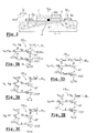
- the present invention is firstly based on the assumption that a failure of an access transistor AT is attributable to a breakdown of the gate oxide.
- the gate of an access transistor AT comprises a gate material 1 (polycrystalline silicon) deposited on a silicon substrate 2, for example of the P - type, via a oxide layer 3.
- Drain and source S regions for example of type N + , are implanted on each side of the gate material 1. These drain and source regions are respectively connected, by means of metal contacts M1 and M2, to a bit line BL j and to the drain D of a floating gate transistor FGT.
- a breakdown of the oxide layer 3 results in the appearance of a leakage resistance Rd, the value of which can be estimated on the order of a few hundred K ⁇ .
- This resistance Rd is shown here in a central position relative to the drain and source regions, but can also appear at the edge of the gate, drain side or source side.
- FIGS. 3A to 3E represent a conventional memory cell CE i, j in five different situations, and illustrate the path followed by the inventors to understand the effects of the breakdown of an access transistor on neighboring memory cells, then to find practical remedies, based on the aforementioned assumption (existence of a leakage resistance Rd). Defects of another type such as the breakdown of a conductive line are not taken into account here.
- the memory cell thus comprises an access transistor AT and a transistor FGT.
- the transistor AT has its gate G connected to a word line selection line WLSL i receiving a control signal V WL , its drain D connected to a bit line BL j receiving a control signal V BL , and its source connected to the drain of the FGT transistor.
- the transistor FGT has its source S connected to a source line SL receiving a control signal V S , and its control gate connected to a gate control line CGL k .
- the line CGL k receives via a gate control transistor CGT k a gate control signal V CG delivered by a column lock LC k (not shown, see fig. 1).
- the transistor CGT k also has its gate connected to the selection line WLSL i .
- the memory cell is in the erasing phase and the control signals have the values mentioned in table 1 appearing in the preamble, column "DELETE".
- a first objective of the invention is thus to remedy this problem.
- the memory cell is in the programming phase and the control signals have the values mentioned in table 1, column "PROGRAMMING".
- the access transistor AT receives the voltage Vpp on its gate and on its drain , its source is at a floating potential (floating signal V S and zero voltage on the control gate of the transistor FGT). Under these conditions, a conductive channel 4 (Cf. fig. 2) appears in the transistor AT. gate oxide of transistor AT is slammed and has a leakage resistance Rd, channel 4 isolates the voltage Vpp present on the gate relative to the silicon substrate 2.
- the memory cell is defective and cannot be read, but the fault n 'prevents by simultaneously programming memory cells belonging to the same word line. There is therefore no contamination of the fault with neighboring cells and the fault can be tolerated.
- the memory cell is not in the programming phase but is connected to a bit line BL j receiving the voltage Vpp because another memory cell connected to this bit line is in the programming phase.
- the access transistor AT has its gate to ground because the word line to which it belongs is not selected. If the gate oxide of the transistor AT is switched on, and the breakdown resistance Rd is on the drain side, the voltage Vpp on the bit line is short-circuited to ground. A current leak occurs which leads to the collapse of the voltage Vpp, preventing the programming of the memory cell connected to the bit line.
- a second objective of the present invention is thus to remedy this problem.
- the memory cell is in the reading phase and the control signals have the values mentioned in table 1, column "READING".
- V S 0
- FGT transistor Vread voltage on the control gate of the FGT transistor.
- a breakdown of the gate oxide layer of the access transistor causes a short circuit between its gate and its conductive channel 4 (fig. 2).
- the state of the access transistor AT, passing or blocked, is uncertain. In any case, the cell is considered to be defective and the bit read therein considered to be invalid.
- the reading fault can be corrected by means of an ECC code, as indicated above. There is therefore no contamination of the effects of the fault on the reading process of the neighboring cells and the fault can be tolerated.
- the memory cell is not in the reading phase but is connected to a bit line BL j receiving the voltage Vsense because another memory cell connected to this bit line is being read.
- the drain of the access transistor AT thus receives the voltage Vsense, while its gate is grounded, the word line not being selected.
- a breakdown of the oxide layer of the access transistor causes a short circuit between the voltage Vsense and the ground, and the appearance of a leakage current which falsifies the detection of the on or off state of the neighboring cell being read. Consequently, any other memory cell connected to the bit line BL j cannot be read correctly.
- this fault can be tolerated and corrected by means of an ECC code, as indicated above, since it concerns only one memory cell per word line.
- the present invention is based here on the observation that applying the voltage Vpp to the gate of a transistor access is useless during the deletion of a word, the process of erasure requiring only the application of voltage Vpp on the control grid of floating gate transistors and the application of an electrical potential of determined value on the source of these transistors, generally the mass. So, according to a first aspect of the present invention, it is proposed to do not apply the voltage Vpp to the grid of the transistors during erasing periods. More specifically, the voltage to be applied to the gate of the transistors access must be such that the voltage Vpp does not collapse during the word erasure, if there is a short circuit between the gate and the source of an access transistor.
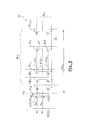
- FIG. 4 is a partial view of a memory 20 according to the invention and represents a word line architecture WL i making it possible to implement the first aspect of the invention.
- a single word W i, k of M memory cells CE i, j is represented on the word line WL i .
- the word W i, k belongs to a column COL k comprising M bit lines BL 0 , ... BL j ... BL M-1 .
- each memory cell comprises a floating gate transistor FGT and an access transistor AT.
- the access transistor AT has its drain connected to a bit line BL j and its source connected to the drain of the transistor FGT, the source of which is connected to a source line SL.
- the control gate of the transistor FGT is connected to a gate control line CGL k which is connected to a column selection line CL k via a gate control transistor CGT k common to all the cells of the word W i, k .
- the column selection line CL k receives a gate control signal V CG delivered by a column lock (not shown), and the control gate of the transistor CGT k is connected to a word line selection line WLSL i .
- the gate of the access transistor AT of each memory cell is not connected to the selection line WLSL 1 .
- the gate of the access transistor AT of each memory cell is in fact connected to a special line ATL i , intended to drive the access transistors.
- the selection line WLSL i is only connected to the gate control transistor CGT k , as well as to the gate control transistors of the other words belonging to the word line WL i (not shown).
- the selection line WLSL i is connected to an output OUT i of a line decoder RDEC1 conventionally delivering a signal V WL of word line selection.
- the REDC1 decoder comprises a second output OUT i ', which is connected to the line ATL i and which delivers a signal V AT ensuring the control of the gates of the access transistors of the word line.
- the signal V AT is identical to the signal V WL during programming or reading phases, and the memory 20 thus operates in a conventional manner in programming and reading.
- the signal V AT is brought to a voltage equal to that of the signal V S located on the source of the floating gate transistors, ie here a zero voltage.
- Table 2 summarizes the values of the control signals during the erasing, programming and reading operations of the memory 20.
- the control signal present on the bit line EL j is designated V BL .
- the voltage Vcc is of the order of 3 to 5V
- the voltage Vpp of the order of 15 to 20V
- the voltage delivered by sense amplifiers is designated Vsense.
- the values mentioned in bold character distinguish the memory according to the invention from a conventional memory. It is clear that in the erasing phase the voltage difference between the signal V AT and the signal V S is zero.
- the advantage of driving the gate control transistors CGT with the voltage Vcc in the programming phase, is to limit the electrical stress undergone by these transistors.
- the implementation of this aspect of the invention requires the addition of the ATL i line, the modification of the electrical connections at the level of the gates of the access transistors. AT, and the provision of an appropriate line decoder.
- FIG. 5 represents a word line architecture WL i similar to the previous one but which can be obtained simply from the topography ("layout") of a conventional memory, with a minimum of modifications.
- the original gate control transistor, designated CGTOLD k is retained but is not connected to the column selection line CL k .
- a new gate control transistor CGT k is added to each word present in the word line WL i .
- the selection line WLSL i is also added, which in practice corresponds to a metallic line passing over the gate of the gate control transistor CGT k (and over the control gates of the transistors CGT k of the other words present on the word line. , not shown here).
- the drain of the unused transistor CGTOLD k can be connected to the drain of the other transistors CGTOLD k present on the other word lines of the memory (not shown).
- this embodiment does not require undoing the original connections between the gates of the AT access transistors, since the original WLSL i selection line becomes the ATL i control line reserved for the AT access transistors.
- the modifications to be provided for in a conventional RDEC line decoder, in order to obtain the REDC1 decoder according to the invention, are also simple as illustrated in FIG. 6.
- the output OUT i of the RDEC decoder forming the output OUT i of the RDEC1 decoder according to the invention.
- the output OUT i ' which delivers the signal V AT , is formed by the output of a gate A1 of type ET receiving as input the signal V WL and a signal / ERASE.
- the gate A1 is conventionally obtained by the association of an inverting gate I1 and a gate NA1 of the NAND type.
- the signal / ERASE is at 1 (voltage Vpp) during the programming phases, and is also at 1 (voltage Vcc) during the reading phases, so that the signal V AT copies the signal V WL .
- Vpp voltage
- Vcc voltage
- the / ERASE signal is set to 0 so that the V AT signal goes to 0.
- the voltage value of the signal V AT ensuring a zero voltage difference between the gate of an AT transistor and the source of an FGT transistor can also, instead of being ground, be a floating potential. Indeed, if there is a short circuit between the gate and the source of the access transistor, the gate of the access transistor is found at the same electrical potential as the source of the floating gate transistor (V S ), this which is compatible with the application of a floating potential on the ATL i line.
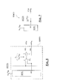
- FIG. 7 represents an RDEC2 decoder according to the invention in which the signal V AT is delivered by the source S of a MOS transistor whose drain D is connected to the output OUT i of the RDEC decoder. The MOS transistor is driven by the signal / ERASE and its drain delivers the control signal V AT which is here floating when the signal / ERASE is at 0.
- the signal V AT can be brought to another value if the voltage V S applied to the source of the floating gate transistors is different from 0.
- certain erasing methods involve a negative source voltage .
- a negative voltage is applied to the gate of the access transistors during the erasing phases.
- a variant of the decoder described above consists in providing, during the programming phases, for the application of the voltage Vcc instead of the voltage Vpp on the gates of the transistors CGT k in order to limit the electrical stress of these transistors, as has already been proposed above.
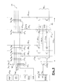
- FIG. 8 is a more extended view of the memory 20.
- the word line architecture WL i according to the invention and the line decoder REDC1 are found there.
- a conventional CDEC column decoder which is connected to the line CL k , and programming locks LPI 1 , ... LPI j ..., LPI M-1 according to l 'invention.
- These locks are connected to the bit lines BL 0 , ... BL j , ... BL M-1 of the column CDL k as well as to a data bus WB allowing the bits to be programmed to be applied to the locks. They also receive a reset signal RST and a column selection signal SCOL k .
- the other elements of the memory are not shown and are, for example, identical to those shown in FIG. 1.
- each programming lock LPI j is slaved in current by a current control circuit ICC, and delivers in the bit line BL j to which it is attached, during a programming phase, a current which cannot exceed a maximum value Imax.
- This maximum value Imax is calculated so that the sum of the currents delivered in each of the bit lines does not exceed the maximum current which can be delivered by the voltage source Vpp, here a charge pump PMP.
- the memory includes n columns of M bit lines each, and that n * M memory cells are programmed simultaneously (programming of a sequence of "0" in a whole page of memory). If the memory is healthy, each bit line is crossed by a nominal current of Iprog programming and the current delivered by the charge pump is equal to n * M * Iprog. If, on the other hand, a bit line includes a slammed access transistor, this bit line is crossed by a leakage current If which is significantly higher than Iprog but which is limited to the Imax value imposed by the programming concerned.
- IPmax the maximum current which can be delivered by the charge pump, it follows that the current Imax imposed in each bit line must be less than: (2) Imax ⁇ [IPmax - n (M-1) Iprog] / n
- Equation (2) It has been assumed for the calculation of equation (2) that we accept at most one defective access transistor per column, and this corresponds to the case where an EEC code is provided to correct one bit and only one per bit chain. However, if an ECC code is used to correct K bits per bit string, relation (2) becomes: (3) Imax ⁇ [IPmax - n (MK) Iprog] / n * K because K erroneous bits can be tolerated in a bit string.
- FIG. 9 represents an exemplary embodiment of the circuit ICC and of a programming lock LPI j according to the invention, in which the principle of the current mirror is used to control the programming current.
- the ICC circuit includes a PMOS transistor TP1 having its gate brought back to its drain, arranged in series with a current generator IGEN imposing a current Imax in the transistor TP1.
- a voltage Vref is taken from the gate of the transistor TP1 and is applied to the programming lock LPI j .
- the lock LPI j conventionally comprises a volatile memory cell formed by two inverting gates INV1, INV2 connected head to tail.
- the input of the gate INV1 is connected to ground via two NMOS transistors TN1, TN2.
- the transistor TN1 receives on the grid a bit b j coming from the data bus WB and the transistor TN2 receives the column selection signal SCOL k .
- the output of gate INV1 is connected to ground via an NMOS transistor TN3, controlled by the reset signal RST.
- the output of gate INV1 is connected to the gate of an NMOS transistor TN4 forming the lock output transistor.
- the transistor TN4 has its source connected to a bit line BL j associated with the latch and its drain receives the voltage Vcc / Vpp, that is to say the voltage Vcc during the loading of the bit b j and the voltage Vpp during the programming phase proper.
- the voltage Vcc / Vpp is applied to the TN4 transistor drain via PMOS transistor TP2, having a width to grid length ratio W / L identical to that of transistor TP1 of the ICC circuit, and forming a current limiter.
- the gate of transistor TP2 receives the signal Vref delivered by the ICC control circuit.
- the output of the gate INV1 switches to 1 and the transistor TN4 turns on.
- the transistor TN4 delivers the voltage Vpp on the bit line BL j and a programming current Iprog flows in the bit line. If the memory cells connected to the bit line BL j are healthy, the current Iprog is of the order of the nanoampere since programming by tunnel effect consumes only a very low current unlike programming by injection of hot carriers (memories Flash).
- a memory cell connected to the bit line BL j has a slammed access transistor, the current delivered in the bit line increases very strongly but is limited by the transistor TP2 to the value Imax, chosen for example from the order of the microampere.
- the present invention can be implemented in combination with the provision of an ECC code making it possible to correct at least one erroneous bit in each word W i, k of the memory.
- the memory obtained will be resistant to faults originating either from an oxide breakdown in an access transistor or in a floating gate transistor. Longer ECC codes can also make it possible to correct in reading faults relating to two or more cells in each word W i, k .
- the present invention is of course capable of various variants within the reach of ordinary skill in the art, both in which concerns the choice of the voltage to be applied on the grids access transistors during erasure periods, the choice of means to apply this tension, and the choice of means to limit the current of Iprog programming in bit lines during periods programming.
- the present invention is also applicable to various EEPROM memory structures.
- the method according to the invention is also applicable to a word programmable memory, does not including that M programming locks.
- the current limiters according to the invention are arranged in the M locks or in the lines connecting each lock at the output of the voltage source Vpp.
Landscapes
- Engineering & Computer Science (AREA)
- Microelectronics & Electronic Packaging (AREA)
- Read Only Memory (AREA)
- Semiconductor Memories (AREA)
Applications Claiming Priority (2)
| Application Number | Priority Date | Filing Date | Title |
|---|---|---|---|
| FR0108347A FR2826496A1 (fr) | 2001-06-25 | 2001-06-25 | Memoire eeprom protegee contre les effets d'un claquage de transistor d'acces |
| FR0108347 | 2001-06-25 |
Publications (2)
| Publication Number | Publication Date |
|---|---|
| EP1278201A2 true EP1278201A2 (de) | 2003-01-22 |
| EP1278201A3 EP1278201A3 (de) | 2005-04-06 |
Family
ID=8864728
Family Applications (2)
| Application Number | Title | Priority Date | Filing Date |
|---|---|---|---|
| EP02358013A Expired - Lifetime EP1278199B1 (de) | 2001-06-25 | 2002-06-25 | Gegen Zugrifftransistordurchschlag geschützter EEPROM-Speicher |
| EP02358012A Withdrawn EP1278201A3 (de) | 2001-06-25 | 2002-06-25 | EEPROM mit gesteuerten Programmierstrom |
Family Applications Before (1)
| Application Number | Title | Priority Date | Filing Date |
|---|---|---|---|
| EP02358013A Expired - Lifetime EP1278199B1 (de) | 2001-06-25 | 2002-06-25 | Gegen Zugrifftransistordurchschlag geschützter EEPROM-Speicher |
Country Status (4)
| Country | Link |
|---|---|
| US (1) | US6934192B2 (de) |
| EP (2) | EP1278199B1 (de) |
| DE (1) | DE60237864D1 (de) |
| FR (1) | FR2826496A1 (de) |
Families Citing this family (17)
| Publication number | Priority date | Publication date | Assignee | Title |
|---|---|---|---|---|
| FR2826496A1 (fr) * | 2001-06-25 | 2002-12-27 | St Microelectronics Sa | Memoire eeprom protegee contre les effets d'un claquage de transistor d'acces |
| JP4426868B2 (ja) * | 2003-04-04 | 2010-03-03 | 株式会社ルネサステクノロジ | 不揮発性半導体記憶装置および半導体集積回路装置 |
| US7057940B2 (en) * | 2003-08-19 | 2006-06-06 | Powerchip Semiconductor Corp. | Flash memory cell, flash memory cell array and manufacturing method thereof |
| JP4153856B2 (ja) * | 2003-09-30 | 2008-09-24 | 株式会社東芝 | 不揮発性半導体記憶装置 |
| US20090003074A1 (en) * | 2006-03-30 | 2009-01-01 | Catalyst Semiconductor, Inc. | Scalable Electrically Eraseable And Programmable Memory (EEPROM) Cell Array |
| US7547944B2 (en) * | 2006-03-30 | 2009-06-16 | Catalyst Semiconductor, Inc. | Scalable electrically eraseable and programmable memory (EEPROM) cell array |
| US8139408B2 (en) * | 2006-09-05 | 2012-03-20 | Semiconductor Components Industries, L.L.C. | Scalable electrically eraseable and programmable memory |
| US8750041B2 (en) | 2006-09-05 | 2014-06-10 | Semiconductor Components Industries, Llc | Scalable electrically erasable and programmable memory |
| US8320191B2 (en) | 2007-08-30 | 2012-11-27 | Infineon Technologies Ag | Memory cell arrangement, method for controlling a memory cell, memory array and electronic device |
| FR2938109A1 (fr) | 2008-11-05 | 2010-05-07 | St Microelectronics Rousset | Memoire eeprom protegee contre les effets de claquage de transistors mos |
| EP2302635B1 (de) * | 2009-09-18 | 2016-01-13 | STMicroelectronics Srl | Verfahren zum Vormagnetisieren einer nichtflüchtigen EEPROM-Speicheranordnung und entsprechende nichtflüchtige EEPROM-Speicheranordnung |
| FR2980025A1 (fr) | 2011-09-12 | 2013-03-15 | St Microelectronics Rousset | Memoire eeprom protegee contre le claquage de transistors de controle de grille |
| FR3021806B1 (fr) * | 2014-05-28 | 2017-09-01 | St Microelectronics Sa | Procede de programmation d'une cellule memoire non volatile comprenant une grille de transistor de selection partagee |
| FR3054723A1 (fr) | 2016-07-27 | 2018-02-02 | Stmicroelectronics (Rousset) Sas | Cellule-memoire eeprom compacte avec zone d'injection tunnel reduite |
| FR3069376B1 (fr) | 2017-07-21 | 2020-07-03 | Stmicroelectronics (Rousset) Sas | Transistor comprenant une grille elargie |
| FR3069374B1 (fr) | 2017-07-21 | 2020-01-17 | Stmicroelectronics (Rousset) Sas | Transistor mos a effet bosse reduit |
| FR3069377B1 (fr) * | 2017-07-21 | 2020-07-03 | Stmicroelectronics (Rousset) Sas | Transistor mos a double blocs de grille a tension de claquage augmentee |
Citations (1)
| Publication number | Priority date | Publication date | Assignee | Title |
|---|---|---|---|---|
| EP1278199B1 (de) * | 2001-06-25 | 2010-10-06 | STMicroelectronics SA | Gegen Zugrifftransistordurchschlag geschützter EEPROM-Speicher |
Family Cites Families (12)
| Publication number | Priority date | Publication date | Assignee | Title |
|---|---|---|---|---|
| US4254477A (en) * | 1978-10-25 | 1981-03-03 | Mcdonnell Douglas Corporation | Reconfigurable memory circuit |
| JPS63153799A (ja) * | 1986-08-08 | 1988-06-27 | Nec Corp | 半導体メモリ |
| KR940005695B1 (ko) * | 1990-12-19 | 1994-06-22 | 삼성전자 주식회사 | 불휘발성 기억소자의 로우 디코더 회로 |
| US5414286A (en) * | 1992-03-19 | 1995-05-09 | Sharp Kabushiki Kaisha | Nonvolatile memory, method of fabricating the same, and method of reading information from the same |
| KR100413652B1 (ko) * | 1995-09-11 | 2004-05-27 | 마츠시타 덴끼 산교 가부시키가이샤 | 반도체기억장치및그구동방법 |
| DE19730116C2 (de) * | 1997-07-14 | 2001-12-06 | Infineon Technologies Ag | Halbleiterspeicher mit nicht-flüchtigen Zwei-Transistor-Speicherzellen |
| US5981340A (en) * | 1997-09-29 | 1999-11-09 | Motorola, Inc. | Method of building an EPROM cell without drain disturb and reduced select gate resistance |
| FR2769747B1 (fr) * | 1997-10-15 | 2001-10-05 | Sgs Thomson Microelectronics | Perfectionnement aux memoires non volatiles programmables par effet dit "de porteurs chauds" et effacables par effet tunnel |
| US5995423A (en) * | 1998-02-27 | 1999-11-30 | Micron Technology, Inc. | Method and apparatus for limiting bitline current |
| US6114724A (en) * | 1998-03-31 | 2000-09-05 | Cypress Semiconductor Corporation | Nonvolatile semiconductor memory cell with select gate |
| US5862082A (en) * | 1998-04-16 | 1999-01-19 | Xilinx, Inc. | Two transistor flash EEprom cell and method of operating same |
| US6501684B1 (en) * | 1999-09-24 | 2002-12-31 | Azalea Microelectronics Corporation | Integrated circuit having an EEPROM and flash EPROM |
-
2001
- 2001-06-25 FR FR0108347A patent/FR2826496A1/fr active Pending
-
2002
- 2002-06-24 US US10/178,796 patent/US6934192B2/en not_active Expired - Lifetime
- 2002-06-25 DE DE60237864T patent/DE60237864D1/de not_active Expired - Lifetime
- 2002-06-25 EP EP02358013A patent/EP1278199B1/de not_active Expired - Lifetime
- 2002-06-25 EP EP02358012A patent/EP1278201A3/de not_active Withdrawn
Patent Citations (1)
| Publication number | Priority date | Publication date | Assignee | Title |
|---|---|---|---|---|
| EP1278199B1 (de) * | 2001-06-25 | 2010-10-06 | STMicroelectronics SA | Gegen Zugrifftransistordurchschlag geschützter EEPROM-Speicher |
Also Published As
| Publication number | Publication date |
|---|---|
| EP1278199B1 (de) | 2010-10-06 |
| US20030035329A1 (en) | 2003-02-20 |
| US6934192B2 (en) | 2005-08-23 |
| DE60237864D1 (de) | 2010-11-18 |
| FR2826496A1 (fr) | 2002-12-27 |
| EP1278199A3 (de) | 2005-03-30 |
| EP1278199A2 (de) | 2003-01-22 |
| EP1278201A3 (de) | 2005-04-06 |
Similar Documents
| Publication | Publication Date | Title |
|---|---|---|
| EP1278199B1 (de) | Gegen Zugrifftransistordurchschlag geschützter EEPROM-Speicher | |
| EP1342244B1 (de) | Seitenlöschbarer flash-speicher | |
| EP0300885B1 (de) | Integrierte Speicherschaltung, die eine Antibetrugseinrichtung einschliesst | |
| EP0568439B1 (de) | Detektionsverfahren und -schaltung für Stromverluste in einer Bitleitung | |
| FR2640797A1 (fr) | Dispositif de memoire electriquement effacable programmable a semi-conducteur et procede pour l'effacement et la programmation de celui-ci | |
| EP0567356A1 (de) | Vorrichtung und Verfahren zum Löschen von Sektoren eines Flash-EPROM-Speichers | |
| FR2652189A1 (fr) | Memoire eeprom "flash" a effacement par blocs. | |
| FR2716566A1 (fr) | Circuit de sélection d'éléments de mémoire redondants et mémoire "Flash Eeprom" comportant ledit circuit. | |
| EP1898426A2 (de) | Mit Hilfe eines Zeilendecoders löschbarer und programmierbarer Speicher mit Phasenumwandlung | |
| EP2337032A1 (de) | Verfahren zur Programmierung einer nichtflüchtigen elektrisch löschbaren und programmierbaren Speicherzelle und und dementsprechende Speicheranordnung | |
| FR2816750A1 (fr) | Memoire flash comprenant des moyens de controle de la tension de seuil de cellules memoire | |
| EP0278832B1 (de) | Leseschaltung für einen Speicher | |
| EP1727152B1 (de) | EEPROM-Speicherarchitektur | |
| EP2184741B1 (de) | EEPROM-Speicher, der gegen die Durchbrucheffekte von MOS-Transistoren geschützt ist | |
| EP0750313B1 (de) | EEPROM-Speicher, der mit Fowler-Nordheim Effekt programmiert und gelöscht wird | |
| WO2004021361A2 (fr) | Memoire eeprom comprenant un registre non volatile integre dans son plan memoire | |
| EP1248268A1 (de) | Wortweise programmierbarer EEPROM mit Doppelfunktionsspaltenauswahlverriegelungen | |
| EP1630820B1 (de) | Speicherzellenprogrammierverfahren mit Detektion von Transkonduktanzdegradierung | |
| EP1486987B1 (de) | Flash-Speicher mit Mitteln zum Steuern und Auffrischen von Speicherzellen im gelöschten Zustand | |
| FR2802734A1 (fr) | Procede de correction d'un bit dans une chaine de bits | |
| FR3006491A1 (fr) | Procede d’ecriture dans une memoire de type eeprom incluant un rafraichissement de cellules memoire | |
| EP3896695B1 (de) | Verfahren zum schreiben in einen nichtflüchtigen speicher in abhängigkeit von der alterung der speicherzellen und entsprechender integrierter schaltkreis | |
| EP2320427A1 (de) | Speichervorrichtung vom elektrisch programmierbaren und löschbaren Typ mit zwei Zellen pro Bit | |
| EP1158408B1 (de) | EEPROM Speicher mit Fehlerkorrekturvorrichtung | |
| FR2769747A1 (fr) | Perfectionnement aux memoires non volatiles programmables par effet dit "de porteurs chauds" et effacables par effet tunnel |
Legal Events
| Date | Code | Title | Description |
|---|---|---|---|
| PUAI | Public reference made under article 153(3) epc to a published international application that has entered the european phase |
Free format text: ORIGINAL CODE: 0009012 |
|
| AK | Designated contracting states |
Kind code of ref document: A2 Designated state(s): AT BE CH CY DE DK ES FI FR GB GR IE IT LI LU MC NL PT SE TR |
|
| AX | Request for extension of the european patent |
Free format text: AL;LT;LV;MK;RO;SI |
|
| RAP1 | Party data changed (applicant data changed or rights of an application transferred) |
Owner name: STMICROELECTRONICS SA |
|
| PUAL | Search report despatched |
Free format text: ORIGINAL CODE: 0009013 |
|
| AK | Designated contracting states |
Kind code of ref document: A3 Designated state(s): AT BE CH CY DE DK ES FI FR GB GR IE IT LI LU MC NL PT SE TR |
|
| AX | Request for extension of the european patent |
Extension state: AL LT LV MK RO SI |
|
| RIC1 | Information provided on ipc code assigned before grant |
Ipc: 7G 11C 16/24 B Ipc: 7G 11C 16/10 B Ipc: 7G 11C 16/04 A |
|
| 17P | Request for examination filed |
Effective date: 20050912 |
|
| AKX | Designation fees paid |
Designated state(s): DE FR GB IT |
|
| 17Q | First examination report despatched |
Effective date: 20071123 |
|
| STAA | Information on the status of an ep patent application or granted ep patent |
Free format text: STATUS: THE APPLICATION IS DEEMED TO BE WITHDRAWN |
|
| 18D | Application deemed to be withdrawn |
Effective date: 20121130 |