EP1278230A2 - Duale Wafer Ladungsschleuse - Google Patents
Duale Wafer Ladungsschleuse Download PDFInfo
- Publication number
- EP1278230A2 EP1278230A2 EP02254961A EP02254961A EP1278230A2 EP 1278230 A2 EP1278230 A2 EP 1278230A2 EP 02254961 A EP02254961 A EP 02254961A EP 02254961 A EP02254961 A EP 02254961A EP 1278230 A2 EP1278230 A2 EP 1278230A2
- Authority
- EP
- European Patent Office
- Prior art keywords
- substrate
- disposed
- chamber
- environment
- substrate holder
- Prior art date
- Legal status (The legal status is an assumption and is not a legal conclusion. Google has not performed a legal analysis and makes no representation as to the accuracy of the status listed.)
- Withdrawn
Links
Images


Classifications
-
- H—ELECTRICITY
- H10—SEMICONDUCTOR DEVICES; ELECTRIC SOLID-STATE DEVICES NOT OTHERWISE PROVIDED FOR
- H10P—GENERIC PROCESSES OR APPARATUS FOR THE MANUFACTURE OR TREATMENT OF DEVICES COVERED BY CLASS H10
- H10P72/00—Handling or holding of wafers, substrates or devices during manufacture or treatment thereof
- H10P72/04—Apparatus for manufacture or treatment
- H10P72/0451—Apparatus for manufacturing or treating in a plurality of work-stations
- H10P72/0452—Apparatus for manufacturing or treating in a plurality of work-stations characterised by the layout of the process chambers
- H10P72/0454—Apparatus for manufacturing or treating in a plurality of work-stations characterised by the layout of the process chambers surrounding a central transfer chamber
-
- H—ELECTRICITY
- H10—SEMICONDUCTOR DEVICES; ELECTRIC SOLID-STATE DEVICES NOT OTHERWISE PROVIDED FOR
- H10P—GENERIC PROCESSES OR APPARATUS FOR THE MANUFACTURE OR TREATMENT OF DEVICES COVERED BY CLASS H10
- H10P72/00—Handling or holding of wafers, substrates or devices during manufacture or treatment thereof
- H10P72/04—Apparatus for manufacture or treatment
- H10P72/0402—Apparatus for fluid treatment
-
- H—ELECTRICITY
- H10—SEMICONDUCTOR DEVICES; ELECTRIC SOLID-STATE DEVICES NOT OTHERWISE PROVIDED FOR
- H10P—GENERIC PROCESSES OR APPARATUS FOR THE MANUFACTURE OR TREATMENT OF DEVICES COVERED BY CLASS H10
- H10P72/00—Handling or holding of wafers, substrates or devices during manufacture or treatment thereof
- H10P72/04—Apparatus for manufacture or treatment
- H10P72/0451—Apparatus for manufacturing or treating in a plurality of work-stations
- H10P72/0452—Apparatus for manufacturing or treating in a plurality of work-stations characterised by the layout of the process chambers
-
- H—ELECTRICITY
- H10—SEMICONDUCTOR DEVICES; ELECTRIC SOLID-STATE DEVICES NOT OTHERWISE PROVIDED FOR
- H10P—GENERIC PROCESSES OR APPARATUS FOR THE MANUFACTURE OR TREATMENT OF DEVICES COVERED BY CLASS H10
- H10P72/00—Handling or holding of wafers, substrates or devices during manufacture or treatment thereof
- H10P72/04—Apparatus for manufacture or treatment
- H10P72/0451—Apparatus for manufacturing or treating in a plurality of work-stations
- H10P72/0461—Apparatus for manufacturing or treating in a plurality of work-stations characterised by the presence of two or more transfer chambers
-
- H—ELECTRICITY
- H10—SEMICONDUCTOR DEVICES; ELECTRIC SOLID-STATE DEVICES NOT OTHERWISE PROVIDED FOR
- H10P—GENERIC PROCESSES OR APPARATUS FOR THE MANUFACTURE OR TREATMENT OF DEVICES COVERED BY CLASS H10
- H10P72/00—Handling or holding of wafers, substrates or devices during manufacture or treatment thereof
- H10P72/04—Apparatus for manufacture or treatment
- H10P72/0451—Apparatus for manufacturing or treating in a plurality of work-stations
- H10P72/0462—Apparatus for manufacturing or treating in a plurality of work-stations characterised by the construction of the processing chambers, e.g. modular processing chambers
-
- H—ELECTRICITY
- H10—SEMICONDUCTOR DEVICES; ELECTRIC SOLID-STATE DEVICES NOT OTHERWISE PROVIDED FOR
- H10P—GENERIC PROCESSES OR APPARATUS FOR THE MANUFACTURE OR TREATMENT OF DEVICES COVERED BY CLASS H10
- H10P72/00—Handling or holding of wafers, substrates or devices during manufacture or treatment thereof
- H10P72/04—Apparatus for manufacture or treatment
- H10P72/0451—Apparatus for manufacturing or treating in a plurality of work-stations
- H10P72/0464—Apparatus for manufacturing or treating in a plurality of work-stations characterised by the construction of the transfer chamber
-
- H—ELECTRICITY
- H10—SEMICONDUCTOR DEVICES; ELECTRIC SOLID-STATE DEVICES NOT OTHERWISE PROVIDED FOR
- H10P—GENERIC PROCESSES OR APPARATUS FOR THE MANUFACTURE OR TREATMENT OF DEVICES COVERED BY CLASS H10
- H10P72/00—Handling or holding of wafers, substrates or devices during manufacture or treatment thereof
- H10P72/04—Apparatus for manufacture or treatment
- H10P72/0451—Apparatus for manufacturing or treating in a plurality of work-stations
- H10P72/0466—Apparatus for manufacturing or treating in a plurality of work-stations characterised by the construction of the load-lock chamber
-
- H—ELECTRICITY
- H10—SEMICONDUCTOR DEVICES; ELECTRIC SOLID-STATE DEVICES NOT OTHERWISE PROVIDED FOR
- H10P—GENERIC PROCESSES OR APPARATUS FOR THE MANUFACTURE OR TREATMENT OF DEVICES COVERED BY CLASS H10
- H10P72/00—Handling or holding of wafers, substrates or devices during manufacture or treatment thereof
- H10P72/06—Apparatus for monitoring, sorting, marking, testing or measuring
- H10P72/0604—Process monitoring, e.g. flow or thickness monitoring
-
- H—ELECTRICITY
- H10—SEMICONDUCTOR DEVICES; ELECTRIC SOLID-STATE DEVICES NOT OTHERWISE PROVIDED FOR
- H10P—GENERIC PROCESSES OR APPARATUS FOR THE MANUFACTURE OR TREATMENT OF DEVICES COVERED BY CLASS H10
- H10P72/00—Handling or holding of wafers, substrates or devices during manufacture or treatment thereof
- H10P72/30—Handling or holding of wafers, substrates or devices during manufacture or treatment thereof for conveying, e.g. between different workstations
- H10P72/33—Handling or holding of wafers, substrates or devices during manufacture or treatment thereof for conveying, e.g. between different workstations into and out of processing chamber
- H10P72/3304—Handling or holding of wafers, substrates or devices during manufacture or treatment thereof for conveying, e.g. between different workstations into and out of processing chamber characterised by movements or sequence of movements of transfer devices
-
- H—ELECTRICITY
- H10—SEMICONDUCTOR DEVICES; ELECTRIC SOLID-STATE DEVICES NOT OTHERWISE PROVIDED FOR
- H10P—GENERIC PROCESSES OR APPARATUS FOR THE MANUFACTURE OR TREATMENT OF DEVICES COVERED BY CLASS H10
- H10P72/00—Handling or holding of wafers, substrates or devices during manufacture or treatment thereof
- H10P72/04—Apparatus for manufacture or treatment
- H10P72/0431—Apparatus for thermal treatment
- H10P72/0434—Apparatus for thermal treatment mainly by convection
-
- H—ELECTRICITY
- H10—SEMICONDUCTOR DEVICES; ELECTRIC SOLID-STATE DEVICES NOT OTHERWISE PROVIDED FOR
- H10P—GENERIC PROCESSES OR APPARATUS FOR THE MANUFACTURE OR TREATMENT OF DEVICES COVERED BY CLASS H10
- H10P72/00—Handling or holding of wafers, substrates or devices during manufacture or treatment thereof
- H10P72/04—Apparatus for manufacture or treatment
- H10P72/0431—Apparatus for thermal treatment
- H10P72/0436—Apparatus for thermal treatment mainly by radiation
Definitions
- This invention generally relates to a method and apparatus for transferring substrates in a semiconductor processing system.
- Semiconductor substrate processing is typically performed by subjecting a substrate to a plurality of sequential processes to create devices, conductors and insulators on the substrate. These processes are generally performed in a process chamber configured to perform a single step of the production process. In order to efficiently complete the entire sequence of processing steps, a number of process chambers are typically coupled to a central transfer chamber that houses a robot to facilitate transfer of the substrate between the surrounding process chambers.
- a semiconductor processing platform having this configuration is generally known as a cluster tool, examples of which are the families of PRODUCER®, CENTURA® and ENDURA® processing platforms available from Applied Materials, Inc., of Santa Clara, California.
- a cluster tool consists of a central transfer chamber having a robot disposed therein.
- the transfer chamber is generally surrounded by one or more process chambers.
- the process chambers are generally utilized to sequentially process the substrate, for example, by performing various processing steps such as etching, physical vapor deposition, chemical vapor deposition, ion implantation, lithography and the like.
- the transfer chamber is maintained at vacuum pressure as well to eliminate having to repeatedly pump down the process chamber for each substrate transfer. This is partially important as pumping down the transfer chamber may require as much as eight hours to reach operational vacuum levels.
- Load lock chambers are generally used to facilitate transfer of the substrates between the vacuum environment of the transfer chamber and an environment of a factory interface wherein substrates are stored in cassettes.
- the factory interface is typically at or near atmospheric pressure.
- the load lock chambers are selectively isolated from the factory interface and transfer chamber by slit valves.
- at least one slit valve is maintained in a closed position to prevent loss of vacuum in the transfer chamber during substrate transfer through the load lock.
- an interface slit valve is opened while a chamber slit valve is closed to allow an interface robot to transfer substrates between the load lock chamber and the substrate storage cassettes disposed in the factory interface.
- both slit valves are closed as the load lock chamber is evacuated by a pump to a vacuum level substantially equal to that of the transfer chamber.
- the substrate in the evacuated load lock is passed into the transfer chamber by opening the chamber slit valve while the interface slit valve remains closed.
- Processed substrates are returned to the factory interface in the reverse manner, wherein the load lock chamber is vented to substantially equalize the pressure between the load lock chamber and the factory interface.
- a first type is known as a batch-type load lock chamber.
- the batch-type chamber generally holds an entire substrate storage cassette within the chamber.
- the cassette is loaded into the load lock chamber and the chamber is sealed and pumped down to an appropriate vacuum level.
- the chamber is then opened to the transfer chamber so that the robot within the transfer chamber may freely access any of the substrates and storage slots within the cassette until all of the substrates within the cassette have been processed.
- the load lock chamber is isolated from the transfer chamber to facilitate replacing the cassette with another cassette containing substrates to be processed. While the cassettes are being exchanged, the transfer robot typically draws substrates from a cassette disposed in a second load lock chamber coupled to the transfer chamber.
- batch-type load lock chambers are generally a robust and effective system for transferring substrates into the transfer chamber.
- pump-down times are long and the associated pumping hardware is large and costly.
- venting of the large internal volume increases the chance of particulate contamination and condensation on the substrates.
- the second type of load lock chamber is known as a single substrate-type.
- the single substrate-type load lock chamber shuttles one processed and one unprocessed substrate therethrough each time the load lock chamber is pumped down.
- single substrate-type load lock chambers are typically used in tandem. This allows a first load lock chamber to exchange substrates with the transfer chamber while a second load lock chamber exchanges substrates with the factory interface wherein the substrate storage cassettes are positioned.
- Cluster tools often utilize more than one load lock to maintain high substrate transfer rates between the factory interface and the transfer chamber.
- the second load lock occupies a position on the transfer chamber at the expense of an additional process chamber throughput and process versatility is sacrificed.
- an additional process chamber could be utilized in the open facet of the transfer chamber, thus enhancing system throughput and versatility.
- utilizing a single load lock chamber would advantageously reduce the cost of ownership for the system.
- the invention generally provides an apparatus for transferring a substrate between a first environment having a first pressure and a second environment having a vacuum pressure.
- the apparatus comprises a chamber body having a first side wall, a second side wall, a top and a bottom defining a chamber volume therebetween.
- a first port is disposed in the first wall and selectively seals the chamber volume from the first environment.
- a second port is disposed in the second wall and selectively seals the chamber volume from the second environment.
- a temperature control pedestal, a first substrate holder and a second substrate holder are disposed between the top and the bottom of the chamber body. The second substrate holder is disposed between the top of the chamber body and the first substrate holder.
- the temperature control pedestal is disposed between the bottom of the chamber body and the first substrate holder.
- the first port and the second port are sequentially opened and the pressure within the load lock regulated to allow substrates to pass through the load lock chamber.
- a window is disposed in the top of the chamber body that allows a metrology device to view the chamber volume.
- a method for transferring semiconductor substrates between a first environment having a first pressure and a second environment having a vacuum pressure using a single load lock chamber includes transferring a processed substrate from the second environment to a second substrate holder disposed in the chamber, moving a cooling plate to contact the processed substrate, venting the chamber, and removing the processed substrate into the first environment.
- Fig. 1 depicts a plan view of a substrate processing system that includes one embodiment of a load lock chamber of the invention
- Fig. 2 depicts a sectional view of the load lock chamber of Fig. 1;
- Fig. 3 depicts a sectional view of one embodiment of a heater module
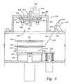
- Fig. 4 depicts a sectional view of another embodiment of a load lock chamber.
- Fig. 1 depicts a processing system 100 that generally includes a factory interface 102, one or more load lock chambers 106, a plurality of process chambers 108 and a substrate transfer chamber 104.
- the transfer chamber 104 is generally used to transfer substrates 124 between a vacuum environment maintained in the transfer chamber 104 and a substantially ambient environment maintained in the factory interface 102.
- One example of a processing system that may be adapted to benefit from the invention is an ENDURA SL® processing platform, available from Applied Materials, Inc., of Santa Clara, California.
- the load lock chamber 106 is described in reference to the exemplary processing system 100 depicted in Fig. 1, the load lock chamber 106 has utility in other systems or wherever transfer of substrates between vacuum and ambient environments is desired.
- the factory interface 102 generally includes an interface robot 120 and a plurality of bays 128. Each bay 128 is adapted to receive a substrate storage cassette 130. Generally, the factory interface 102 is coupled to the load lock chamber 106 through a side wall 136 that is positioned opposite the bays 128.
- the interface robot 120 is disposed in an interior volume 116 of the factory interface 102 that is maintained at a substantially ambient pressure.
- the interface robot 120 includes at least a first gripper 110 coupled thereto. Generally, the first gripper 110 may be an edge gripper, vacuum gripper or other substrate securing device used to hold the substrate 124 during transfer.
- the interface robot 120 is generally positioned between the side wall 136 and bays 128 to facilitate transfer of substrates between the cassettes 130 and the load lock 106.
- An example of one factory interface that may be adapted to benefit from the invention is described in United States Patent Application No. 09/161,970, filed September 28, 1998 by Kroeker, which is hereby incorporated by reference in its entirety.
- the transfer chamber 104 is generally fabricated from a single piece of material such as aluminum.
- the transfer chamber 104 generally includes side walls 150 and chamber bottom 156.
- a lid 138 (shown in Fig. 2) is supported by the side walls 150 and, with the side wall 150 and chamber bottom 156, define an evacuable interior volume 122 therebetween.
- Substrates 124 are transferred between the process chambers 108 and load lock chambers 106 coupled to the exterior of the chamber 104 through the vacuum maintained within the volume 122.
- At least one transfer robot 112 is disposed in the transfer chamber 104 to facilitate transfer of substrates between the process chambers 108.
- the transfer robot 112 has at least one end effector such as a gripper or a blade 114 for securing the substrate during transfer.
- the transfer robot 112 typically has a "frog-leg" linkage that is commonly used to transfer substrates in vacuum environments.
- the transfer robot 112 is generally disposed in the interior volume 122 of the transfer chamber 104 and has a range of motion that allows the substrate 124 to be transferred between the load lock 106 and the process chambers 108.
- the transfer chamber 104 includes two transfer robots 112 each having dual blades 114.
- the process chambers 108 are typically fastened to an exterior side 152 of the side walls 150 of the transfer chamber 104.
- Examples of process chambers 108 that may be utilized are etching chambers, physical vapor deposition chambers, chemical vapor deposition chambers, ion implantation chambers, lithography chambers and the like.
- Different process chambers 108 may be coupled to the transfer chamber 104 to provide a processing sequence necessary to form a predefined structure or feature upon the substrate's surface.
- An aperture (not shown) is disposed in the side wall between each process chamber 108 (or other chambers) to allow the substrate to be passed between the process chamber 108 and interior volume 122 of the transfer chamber 104.
- a slit valve 132 selectively seals each aperture to maintain isolation between the environments of the chambers 108, 104 between substrate transfers and during processing within the process chambers 108.
- One slit valve that may be used to advantage is described in United States Patent No. 5,226,632, issued July 13, 1993 to Tepman, et al., which is hereby incorporated by reference in its entirety.
- a pumping system 142 is coupled to the transfer chamber 104 to evacuate and maintain the chamber at a predetermined vacuum level.
- a pumping port 140 is centrally disposed in the chamber bottom 156 to fluidly couple the interior volume 122 to the pumping system 142.
- the pumping system 142 may include one or more pumps such as a roughing pump, a turbomolecular pump or a cryogenic pump.
- the load lock chamber 106 is generally coupled between the factory interface 102 and the transfer chamber 104.
- the load lock chamber 106 is generally used to facilitate transfer of the substrates 124 between a vacuum environment which is maintained in the interior volume 122 of the transfer chamber 104 and an environment of the factory interface 102 rapidly without loss of vacuum within the transfer chamber.
- the load lock chamber 106 generally comprises a chamber body 202, a first substrate holder 204, a second substrate holder 206, a temperature control pedestal 240 and a heater module 270.
- the chamber body 202 is preferably fabricated from a singular body of material such as aluminum.
- the chamber body 202 includes a first side wall 208, a second side wall 210, lateral walls (242 in Fig. 3), a top 214 and a bottom 216 that define a chamber volume 218.
- a window 250 typically comprised of quartz, is disposed in the top 216 of the chamber body 202 and is at least partially covered by the heater module 270.
- the atmosphere of the chamber volume 218 is controlled so that it may be evacuated to substantially match the environment of the transfer chamber 104 and be vented to substantially match the environment of the factory interface 102.
- the chamber body 202 includes a vent passage 230 and a pump passage 232.
- the vent passage 230 and the pump passage 232 are positioned at opposite ends of the chamber body 202 to induce laminar flow within the chamber volume 218 during venting and evacuation to minimize particulate contamination.
- the vent passage 230 is disposed through the top 214 of the chamber body 202 while the pump passage 232 is disposed through the bottom 216 of the chamber body 202.
- the passages 230, 232 typically are coupled to a valve 212 to selectively allow flow into and out of the chamber volume 218.
- the passages 230, 232 may be positioned at opposite ends of one of the chamber walls, or on opposing or adjacent walls.
- the vent passage 230 is coupled to a high efficiency air filter 234 such as available from Camfil-Farr, of Riverdale, New Jersey.
- the pump passage 232 is coupled to a point-of-use pump 236 such as available from Alcatel, headquartered in Paris, France.
- the point-of-use pump 236 has low vibration generation to minimize the disturbance of the substrates 124 positioned within the load lock chamber 106 while promoting pump-down efficiency and time by minimizing the fluid path between the chamber 106 and pump 234 to generally less than three feet.
- a first loading port 238 is disposed in the first wall 208 of the chamber body 202 to allow substrates 124 to be transferred between the load lock 106 and the factory interface 102.
- a first slit valve 244 selectively seals the first loading port 238 to isolate the load lock 106 from the factory interface 102.
- a second loading port 239 is disposed in the second wall 210 of the chamber body 202 to allow substrates 124 to be transferred between the load lock 106 and the transfer chamber 104.
- a second slit valve 146 which is substantially similar to the first slit valve 244 selectively seals the second loading port 239 to isolate the load lock 106 from the vacuum environment of the transfer chamber 104.
- One slit valve that may be used to advantage is described in United States Patent No. 5,226,632, issued July 13, 1993 to Tepman et al., which is hereby incorporated by reference in its entirety.
- the first substrate holder 204 is concentrically coupled to (i.e., stacked on top of) the second substrate holder 206 that is disposed above the chamber bottom 216.
- the substrate holders 204 and 206 are generally mounted to a hoop 220 that is coupled to a shaft 284 that extends through the bottom 216 of the chamber body 202.
- each substrate holder 204, 206 is configured to retain one substrate.
- the shaft 284 is coupled to a lift mechanism 294 that controls the elevation of the substrate holders 204 and 206 within the chamber body 206.
- a bellows 284 is generally disposed around the shaft 284 to prevent leakage from or into the body 206.
- the first substrate holder 204 is utilized to hold an unprocessed substrate while the second substrate holder 206 is utilized to hold a processed substrate returning from the transfer chamber 104.
- the flow within the load lock 106 during venting and evacuation is substantially laminar due to the position of the vent passage 230 and pump passage 232 and is configured to minimize particulate contamination.
- Fig. 3 depicts one embodiment of the substrate holders 204, 206.
- the second substrate holder 206 is generally held above the bottom 216 of the chamber body 202 by the hoop 220.
- a first standoff 308 is disposed between each member 304, 306 to maintain the second substrate holder 206 in a spaced-apart relation to the hoop 220.
- a second standoff 310 is disposed between the first and second substrate holders 204, 206 to maintain a spaced-apart relation therebetween.
- the standoffs 308, 310 allow grippers 110, 114 of the transfer and factory interface robots 112, 120 to pass therebetween when retrieving and depositing substrates on the substrate holders 204, 206.
- each substrate holder 204, 206 includes a first member 304 and a second member 306.
- Each holder 204, 206 may have alternatively include a "L-shaped" configuration that incorporates a portion that maintains a spaced-apart relation between holder 204, 206 and adjacent components of the load lock 106.
- Each member 304, 306 includes a curved inner portion 312 that has a lip 314 extending radially inwards therefrom.
- the curved inner portion 312 is generally configured to allow the substrate 124 to pass therebetween and rest on the lip 314.
- the curved inner portion 312 captures the substrate 124 therebetween, thus preventing the substrate 124 from falling off the lip 314.
- the temperature control pedestal 240 is typically coupled to the bottom 216 of the chamber body 202 by a support 278.
- the support 278 may be hollow or include passages therethrough to allow fluids, electrical signals, sensor and the like to be coupled to the pedestal 240.
- the pedestal 240 may be movably coupled to the chamber body 202.
- the temperature control pedestal 240 generally includes a platen 280 which is generally fabricated from a thermally conductive material such as aluminum or stainless steel but may alternatively be comprised of other materials such as ceramic.
- the platen 280 generally has a heat transfer element 286 such as fluid passage disposed in the platen 280 or disposed in contact with a lower surface 288 of the platen 280.
- the heat transfer element 286 may be a circulated water jacket, a thermoelectric device such as a Peltier device or other structure that may be utilized to control the temperature of the platen 280.
- the heat transfer element 286 comprises a tube 290 disposed proximate the lower surface 288 of the platen 280.
- the tube 290 is coupled to a fluid source 294 that circulates a fluid through the tube.
- the fluid for example facility water from the fluid source 294, may optionally be thermally regulated.
- the tube 290 may be disposed in a substantially circular or spiral pattern against the lower surface 288 of the platen 280.
- the tube 290 is brazed to the lower surface 288 or adhered using a conductive adhesive.
- a conductive plate such as a copper plate may alternatively be disposed between the tube 290 and platen 280 to promote uniformity of heat transfer across the width of the platen 280.
- the hoop 220 having the substrate holders 204, 206 coupled thereto may be lowered to a first position where an upper surface 292 of the platen 280 is in close proximity or in contact with the substrate supported by the second substrate holder 206.
- the platen 280 may be used to regulate the temperature of the substrate disposed on (or proximate to) the platen 280.
- a substrate returning from processing may be cooled in the load lock chamber 106 by supporting the substrate during the evacuation of the chamber 106 on the upper surface 292 of the platen 280. Thermal energy is transferred from the substrate through the platen 280 to the heat transfer element 286, thereby cooling the substrate.
- the substrate holders 204, 206 may be raised towards the top 214 of the chamber body 202 to allow the robots 112, 120 access to the substrate seated in the second substrate support 206.
- the substrate may be heated.
- the holders 204, 206 may be lowered to a position where the upper surface 292 is in contact or close proximity to the substrate supported by the first substrate holder 204. In this position, the platen 280 may be used to thermally regulate the substrate.
- the shaft 282 generally couples the substrate holders 204, 206 to a lift mechanism 296 disposed exterior to the load lock chamber 106.
- the bellows 284 are coupled between the second substrate holder 206 and the bottom 216 of the chamber body 202 and provide a flexible seal therebetween, thus facilitating raising and lowering the substrate holders 204, 206 without compromising the pressure within the load lock chamber 106.
- Fig. 4 depicts a sectional view of one embodiment of the heater module 270.
- the heater module 270 is generally disposed on the top 214 of the load lock chamber 106.
- the heater module 270 may alternatively comprise various types of radiant heaters.
- the heater module 270 includes a housing 402 having a lamp 404 disposed therein.
- the housing 402 generally includes sides 406 and a top 408 that define an interior 430.
- the sides 406 are generally coupled to the top of the chamber body.
- An aperture 412 is disposed in the top 408 of the heater module 270 to facilitate power connection to the lamp 402.
- the lamp 402 is generally coupled to a power source 432 by a ceramic socket 414.
- a cooling device 416 is coupled to the socket 414 to control the temperature rise of the lamp 402 to extend the life of the lamp 402.
- the cooling device 416 is an annular plate 418 having good thermal conductivity that is thermally regulated by a circulating fluid.
- the annular plate 418 is a copper disk having a tube 420 brazed to the perimeter of the plate 418. The fluid is circulated through the tube 420 from a fluid source 434 thereby regulating the temperature of the plate 418.
- the cooling device 416 may include thermoelectric devices, heat sinks, water jackets and other devices that limit the temperature rise of the socket 414.
- the socket 414 is typically biased against the plate 418 to promote heat transfer therebetween.
- a shoulder screw 422 is disposed through the socket 414 and plate 418 and threads into the top 408 of the housing 402.
- one or more springs 424 are disposed between a head 426 of the shoulder screw 422 and the socket 414.
- the spring 424 which may be a coil, flat, belliville or other basising device, maintains contact between the socket 414 and plate 418 over a wide range of temperature without damaging the socket 414.
- Fig. 4 additionally depicts another embodiment of a temperature control pedestal 450.
- the temperature control pedestal 450 is substantially similar to the temperature control pedestal 240 described with reference to Fig. 2 except that the temperature control pedestal 450 rotates.
- the pedestal 450 generally includes an upper portion 452 and a lower portion 454.
- the lower portion is generally stationary and is coupled a bottom 456 of the chamber.
- a rotary actuator 458 is disposed between the upper portion 452 and lower portion 454 of the pedestal 450.
- the rotary actuator 458 generally provides rotary motion to the upper portion 452 of the pedestal 450.
- the upper portion 452 rotates the substrate 124.
- the rotary actuator 458 may be a solenoid, air motor, electric motor or other device that induces rotary motion to the upper portion 452 of the pedestal 450.
- the rotary actuator 458 may be disposed remote to the load lock chamber and configured to rotate the upper portion 452 of the pedestal 450 via a linkage (not shown) disposed through the bottom 456.
- a metrology device 428 is disposed proximate the window.
- the metrology device 428 may be a wafer type sensor, a wafer orientation sensor, a wafer center sensor, a wafer location sensor, a film thickness detector, a topography detector or other device utilized to detect attributes of the substrate disposed in the load lock chamber.
- the metrology device 428 is disposed proximate the heater module 270 and positioned to view the substrate through the window.
- the metrology device 428 may be disposed in the heater module 270.
- the metrology device 428 includes a sensor 490 disposed outside of the chamber 106 and positioned to view the substrate supported on the pedestal 450 through the window 250 disposed in the top 214 of the chamber body 202.
- the sensor 490 projects a beam 492 to the perimeter of the substrate 124.
- the orientation of the substrate is determined by detecting variations in a portion 494 of beam 492 reflected off the substrate due to features such as notches or flats (not shown) in the perimeter of the substrate.
- the load lock 106 generally facilitates the transfer of substrates between the ambient atmosphere of the factory interface and the vacuum atmosphere of the transfer chamber.
- the load lock 106 temporarily houses the substrate while the atmosphere within the load lock 106 is adjusted to match the atmosphere of the chamber into which the substrate is to be transferred.
- the slit valve 244 is opened while the load lock 106 is vented to substantially atmospheric pressure to match the atmosphere of the factory interface 102.
- the factory interface robot 120 transfers an unprocessed substrate from one of the cassettes 130 to the first substrate holder 204.
- a processed substrate is removed from the second substrate holder 206 by the factory interface robot 120 and returned to one of the cassettes 130.
- the slit valve 244 and vent passage 230 are closed.
- the pump passage 232 is opened and the load lock chamber 106 is pumped down to the pressure substantially equal to the pressure of the transfer chamber 104.
- the heater module 270 heats the substrate residing in the first substrate holder 204.
- the metrology device 428 (seen in Fig. 4) may be utilized to determine the substrate's center or other substrate metric.
- the slit valve 246 is opened.
- a processed substrate is positioned in the second substrate holder 206 by the transfer robot 112.
- the transfer robot 112 retrieves the unprocessed substrate for position in the first substrate holder 204 for processing in one or more of the process chambers 108 circumscribing the transfer chamber 104.
- the second slit valve 246 is closed to seal the load lock 106 from the transfer chamber 104.
- the vent passage 230 is opened in the load lock 106 to allow the pressure in the load lock 106 to rise to substantially match the pressure in the factory interface 102. While venting, the pedestal 242 is raised to contact the substrate disposed in the second substrate holder 206. The substrate is cooled by transferring heat through the pedestal 240 to the fluid circulating in the tube 290.
- the metrology device 428 may be utilized to detect a metric of the substrate, for example, surface defeats. Once, the pressures are matched, the first slit valve 244 is opened to allow the factory interface robot 120 to access the load lock 106 as described above.
Landscapes
- Container, Conveyance, Adherence, Positioning, Of Wafer (AREA)
Applications Claiming Priority (2)
| Application Number | Priority Date | Filing Date | Title |
|---|---|---|---|
| US09/906,887 US6558509B2 (en) | 1999-11-30 | 2001-07-16 | Dual wafer load lock |
| US906887 | 2001-07-16 |
Publications (2)
| Publication Number | Publication Date |
|---|---|
| EP1278230A2 true EP1278230A2 (de) | 2003-01-22 |
| EP1278230A3 EP1278230A3 (de) | 2004-02-18 |
Family
ID=25423152
Family Applications (1)
| Application Number | Title | Priority Date | Filing Date |
|---|---|---|---|
| EP02254961A Withdrawn EP1278230A3 (de) | 2001-07-16 | 2002-07-15 | Duale Wafer Ladungsschleuse |
Country Status (3)
| Country | Link |
|---|---|
| US (2) | US6558509B2 (de) |
| EP (1) | EP1278230A3 (de) |
| JP (1) | JP2003068819A (de) |
Cited By (5)
| Publication number | Priority date | Publication date | Assignee | Title |
|---|---|---|---|---|
| EP1860683A3 (de) * | 2006-05-26 | 2011-06-08 | Cree Inc. | Vorrichtung zur Ionenimplantation bei hoher Temperatur und Verfahren zur Herstellung von Halbleitervorrichtungen unter Verwendung von Ionenimplantation bei hoher Temperatur |
| EP2261391A4 (de) * | 2008-03-25 | 2013-01-23 | Orbotech Lt Solar Llc | Verarbeitungsvorrichtung und verarbeitungsverfahren |
| US8672603B2 (en) | 2009-12-10 | 2014-03-18 | Orbotech LT Solar, LLC. | Auto-sequencing inline processing apparatus |
| US8998552B2 (en) | 2007-10-23 | 2015-04-07 | Orbotech LT Solar, LLC. | Processing apparatus and processing method |
| US9462921B2 (en) | 2011-05-24 | 2016-10-11 | Orbotech LT Solar, LLC. | Broken wafer recovery system |
Families Citing this family (104)
| Publication number | Priority date | Publication date | Assignee | Title |
|---|---|---|---|---|
| US6672819B1 (en) * | 1995-07-19 | 2004-01-06 | Hitachi, Ltd. | Vacuum processing apparatus and semiconductor manufacturing line using the same |
| JPH0936198A (ja) * | 1995-07-19 | 1997-02-07 | Hitachi Ltd | 真空処理装置およびそれを用いた半導体製造ライン |
| US6949143B1 (en) | 1999-12-15 | 2005-09-27 | Applied Materials, Inc. | Dual substrate loadlock process equipment |
| EP1319243A2 (de) * | 2000-09-15 | 2003-06-18 | Applied Materials, Inc. | Zweifachladungsschleusenvorrichtung mit doppelschlitz für prozessanlage |
| US7316966B2 (en) * | 2001-09-21 | 2008-01-08 | Applied Materials, Inc. | Method for transferring substrates in a load lock chamber |
| US6936906B2 (en) * | 2001-09-26 | 2005-08-30 | Applied Materials, Inc. | Integration of barrier layer and seed layer |
| US6916398B2 (en) * | 2001-10-26 | 2005-07-12 | Applied Materials, Inc. | Gas delivery apparatus and method for atomic layer deposition |
| US20030086774A1 (en) * | 2001-11-07 | 2003-05-08 | Schlumberger Technologies, Inc. | System and method for inhibiting motion of semiconductor wafers in a variable-pressure chamber |
| US6972267B2 (en) * | 2002-03-04 | 2005-12-06 | Applied Materials, Inc. | Sequential deposition of tantalum nitride using a tantalum-containing precursor and a nitrogen-containing precursor |
| US6797067B1 (en) * | 2002-05-17 | 2004-09-28 | Macronix International Co., Ltd. | Implanter tool process parameter auto pre-setup system |
| US6896513B2 (en) | 2002-09-12 | 2005-05-24 | Applied Materials, Inc. | Large area substrate processing system |
| EP1420080A3 (de) * | 2002-11-14 | 2005-11-09 | Applied Materials, Inc. | Vorrichtung und Verfahren zu hybriden chemischen Abscheidungsverfahren |
| SG115629A1 (en) | 2003-03-11 | 2005-10-28 | Asml Netherlands Bv | Method and apparatus for maintaining a machine part |
| SG115631A1 (en) | 2003-03-11 | 2005-10-28 | Asml Netherlands Bv | Lithographic projection assembly, load lock and method for transferring objects |
| KR100441875B1 (ko) * | 2003-06-02 | 2004-07-27 | 주성엔지니어링(주) | 분리형 이송 챔버 |
| US7207766B2 (en) * | 2003-10-20 | 2007-04-24 | Applied Materials, Inc. | Load lock chamber for large area substrate processing system |
| US20050095859A1 (en) * | 2003-11-03 | 2005-05-05 | Applied Materials, Inc. | Precursor delivery system with rate control |
| US20070269297A1 (en) | 2003-11-10 | 2007-11-22 | Meulen Peter V D | Semiconductor wafer handling and transport |
| US8403613B2 (en) * | 2003-11-10 | 2013-03-26 | Brooks Automation, Inc. | Bypass thermal adjuster for vacuum semiconductor processing |
| US10086511B2 (en) | 2003-11-10 | 2018-10-02 | Brooks Automation, Inc. | Semiconductor manufacturing systems |
| JP2005158926A (ja) * | 2003-11-25 | 2005-06-16 | Canon Inc | ロードロック装置および方法 |
| JP4280159B2 (ja) * | 2003-12-12 | 2009-06-17 | 東京エレクトロン株式会社 | 基板処理装置 |
| US20050133158A1 (en) * | 2003-12-19 | 2005-06-23 | Applied Materials, Inc. | Mask handler apparatus |
| US20060185793A1 (en) * | 2004-01-11 | 2006-08-24 | Tokyo Electron Limited | Substrate processing system |
| JP2005262367A (ja) * | 2004-03-18 | 2005-09-29 | Tokyo Electron Ltd | 搬送ロボットの搬送ズレ確認方法及び処理装置 |
| US20050252449A1 (en) * | 2004-05-12 | 2005-11-17 | Nguyen Son T | Control of gas flow and delivery to suppress the formation of particles in an MOCVD/ALD system |
| US7497414B2 (en) * | 2004-06-14 | 2009-03-03 | Applied Materials, Inc. | Curved slit valve door with flexible coupling |
| EP1622195A1 (de) * | 2004-07-21 | 2006-02-01 | Afore Oy | Gerät und Verfahren zur Prüfung von auf Halbleiterchips hergestellte Anordnungen |
| US20060137609A1 (en) * | 2004-09-13 | 2006-06-29 | Puchacz Jerzy P | Multi-single wafer processing apparatus |
| US7314777B2 (en) * | 2004-11-15 | 2008-01-01 | Honeywell International Inc. | Chip packaging systems and methods |
| US20070134821A1 (en) * | 2004-11-22 | 2007-06-14 | Randhir Thakur | Cluster tool for advanced front-end processing |
| US20070196011A1 (en) * | 2004-11-22 | 2007-08-23 | Cox Damon K | Integrated vacuum metrology for cluster tool |
| KR20070089197A (ko) * | 2004-11-22 | 2007-08-30 | 어플라이드 머티어리얼스, 인코포레이티드 | 배치 처리 챔버를 사용한 기판 처리 기기 |
| US20060167583A1 (en) * | 2005-01-22 | 2006-07-27 | Applied Materials, Inc. | Method and apparatus for on the fly positioning and continuous monitoring of a substrate in a chamber |
| US7585141B2 (en) * | 2005-02-01 | 2009-09-08 | Varian Semiconductor Equipment Associates, Inc. | Load lock system for ion beam processing |
| JP4860167B2 (ja) * | 2005-03-30 | 2012-01-25 | 東京エレクトロン株式会社 | ロードロック装置,処理システム及び処理方法 |
| JP4748649B2 (ja) * | 2005-04-15 | 2011-08-17 | キヤノン株式会社 | 駆動装置 |
| US20060273815A1 (en) * | 2005-06-06 | 2006-12-07 | Applied Materials, Inc. | Substrate support with integrated prober drive |
| KR20070004230A (ko) * | 2005-07-04 | 2007-01-09 | 삼성전자주식회사 | 반도체 웨이퍼 이송용 로봇 |
| US20070006936A1 (en) * | 2005-07-07 | 2007-01-11 | Applied Materials, Inc. | Load lock chamber with substrate temperature regulation |
| US20070020890A1 (en) * | 2005-07-19 | 2007-01-25 | Applied Materials, Inc. | Method and apparatus for semiconductor processing |
| US7470919B2 (en) * | 2005-09-30 | 2008-12-30 | Applied Materials, Inc. | Substrate support assembly with thermal isolating plate |
| KR101019293B1 (ko) * | 2005-11-04 | 2011-03-07 | 어플라이드 머티어리얼스, 인코포레이티드 | 플라즈마-강화 원자층 증착 장치 및 방법 |
| CN100388456C (zh) * | 2005-12-08 | 2008-05-14 | 北京圆合电子技术有限责任公司 | 一种真空锁过渡腔室 |
| US7845891B2 (en) * | 2006-01-13 | 2010-12-07 | Applied Materials, Inc. | Decoupled chamber body |
| US20070252299A1 (en) * | 2006-04-27 | 2007-11-01 | Applied Materials, Inc. | Synchronization of precursor pulsing and wafer rotation |
| US7798096B2 (en) * | 2006-05-05 | 2010-09-21 | Applied Materials, Inc. | Plasma, UV and ion/neutral assisted ALD or CVD in a batch tool |
| US20070259111A1 (en) * | 2006-05-05 | 2007-11-08 | Singh Kaushal K | Method and apparatus for photo-excitation of chemicals for atomic layer deposition of dielectric film |
| US7665951B2 (en) * | 2006-06-02 | 2010-02-23 | Applied Materials, Inc. | Multiple slot load lock chamber and method of operation |
| US7845618B2 (en) | 2006-06-28 | 2010-12-07 | Applied Materials, Inc. | Valve door with ball coupling |
| US8124907B2 (en) * | 2006-08-04 | 2012-02-28 | Applied Materials, Inc. | Load lock chamber with decoupled slit valve door seal compartment |
| US7655571B2 (en) * | 2006-10-26 | 2010-02-02 | Applied Materials, Inc. | Integrated method and apparatus for efficient removal of halogen residues from etched substrates |
| KR100765188B1 (ko) | 2006-11-30 | 2007-10-15 | 세메스 주식회사 | 기판 이송 장치, 기판 처리 장치 및 기판 처리 방법 |
| US20080138178A1 (en) * | 2006-12-06 | 2008-06-12 | Axcelis Technologies,Inc. | High throughput serial wafer handling end station |
| US7880598B2 (en) * | 2006-12-08 | 2011-02-01 | International Business Machines Corporation | Six face, multi-event, orientation sensor |
| US8821637B2 (en) * | 2007-01-29 | 2014-09-02 | Applied Materials, Inc. | Temperature controlled lid assembly for tungsten nitride deposition |
| JP2008192642A (ja) * | 2007-01-31 | 2008-08-21 | Tokyo Electron Ltd | 基板処理装置 |
| US20080206022A1 (en) * | 2007-02-27 | 2008-08-28 | Smith John M | Mult-axis robot arms in substrate vacuum processing tool |
| US20080206036A1 (en) * | 2007-02-27 | 2008-08-28 | Smith John M | Magnetic media processing tool with storage bays and multi-axis robot arms |
| KR100839191B1 (ko) * | 2007-03-28 | 2008-06-17 | 세메스 주식회사 | 기판 처리 장치 및 방법 |
| US20080276867A1 (en) | 2007-05-09 | 2008-11-13 | Jason Schaller | Transfer chamber with vacuum extension for shutter disks |
| US10541157B2 (en) | 2007-05-18 | 2020-01-21 | Brooks Automation, Inc. | Load lock fast pump vent |
| TWI455861B (zh) * | 2007-05-18 | 2014-10-11 | Brooks Automation Inc | 基板加工工具、半導體加工工具、及基板加工裝置 |
| US8272825B2 (en) | 2007-05-18 | 2012-09-25 | Brooks Automation, Inc. | Load lock fast pump vent |
| KR100868795B1 (ko) | 2007-05-23 | 2008-11-17 | 세메스 주식회사 | 반도체 소자 제조용 로드 락 챔버 |
| US8033769B2 (en) | 2007-11-30 | 2011-10-11 | Novellus Systems, Inc. | Loadlock designs and methods for using same |
| KR20100108364A (ko) * | 2007-12-20 | 2010-10-06 | 어플라이드 머티어리얼스, 인코포레이티드 | 이송 모듈 상의 하나의 단일한 면을 사용하는 엇갈린 이중 처리 챔버 |
| JP5108557B2 (ja) * | 2008-02-27 | 2012-12-26 | 東京エレクトロン株式会社 | ロードロック装置および基板冷却方法 |
| US9117870B2 (en) * | 2008-03-27 | 2015-08-25 | Lam Research Corporation | High throughput cleaner chamber |
| US8288288B1 (en) | 2008-06-16 | 2012-10-16 | Novellus Systems, Inc. | Transferring heat in loadlocks |
| WO2011075110A1 (en) * | 2008-11-19 | 2011-06-23 | Brooks Automation, Inc. | Process chamber with intergrated pumping |
| US8033771B1 (en) | 2008-12-11 | 2011-10-11 | Novellus Systems, Inc. | Minimum contact area wafer clamping with gas flow for rapid wafer cooling |
| GB2483421B (en) * | 2009-06-24 | 2013-10-09 | Canon Anelva Corp | Vacuum heating/cooling apparatus and manufacturing method of magnetoresistance element |
| JP5358366B2 (ja) * | 2009-09-14 | 2013-12-04 | 東京エレクトロン株式会社 | 基板処理装置及び方法 |
| US8562272B2 (en) | 2010-02-16 | 2013-10-22 | Lam Research Corporation | Substrate load and unload mechanisms for high throughput |
| US8893642B2 (en) | 2010-03-24 | 2014-11-25 | Lam Research Corporation | Airflow management for low particulate count in a process tool |
| US8282698B2 (en) | 2010-03-24 | 2012-10-09 | Lam Research Corporation | Reduction of particle contamination produced by moving mechanisms in a process tool |
| US20110269314A1 (en) * | 2010-04-30 | 2011-11-03 | Applied Materials, Inc. | Process chambers having shared resources and methods of use thereof |
| DE102010048043A1 (de) | 2010-10-15 | 2012-04-19 | Ev Group Gmbh | Vorrichtung und Verfahren zur Prozessierung von Wafern |
| JP2011054998A (ja) * | 2010-11-30 | 2011-03-17 | Tokyo Electron Ltd | 真空処理装置及び真空処理方法並びに記憶媒体 |
| US9111971B2 (en) * | 2012-07-30 | 2015-08-18 | Applied Materials Israel, Ltd. | System and method for temperature control of a semiconductor wafer |
| KR101990555B1 (ko) * | 2012-12-24 | 2019-06-19 | 삼성디스플레이 주식회사 | 박막봉지 제조장치 및 박막봉지 제조방법 |
| TWI624897B (zh) | 2013-03-15 | 2018-05-21 | Applied Materials, Inc. | 多位置批次負載鎖定裝置與系統,以及包括該裝置與系統的方法 |
| CN105580124B (zh) * | 2013-09-26 | 2018-05-18 | 应用材料公司 | 用于基板处理的混合平台式设备、系统以及方法 |
| KR20150078549A (ko) * | 2013-12-31 | 2015-07-08 | 한국과학기술원 | 집적형 박막 태양전지의 제조 장치 |
| US9378992B2 (en) | 2014-06-27 | 2016-06-28 | Axcelis Technologies, Inc. | High throughput heated ion implantation system and method |
| US9607803B2 (en) | 2015-08-04 | 2017-03-28 | Axcelis Technologies, Inc. | High throughput cooled ion implantation system and method |
| US10304707B2 (en) * | 2015-10-20 | 2019-05-28 | Lam Research Corporation | Load lock interface and integrated post-processing module |
| US10014196B2 (en) | 2015-10-20 | 2018-07-03 | Lam Research Corporation | Wafer transport assembly with integrated buffers |
| US9502275B1 (en) | 2015-10-20 | 2016-11-22 | Lam Research Corporation | Service tunnel for use on capital equipment in semiconductor manufacturing and research fabs |
| JP6863041B2 (ja) * | 2017-04-21 | 2021-04-21 | 東京エレクトロン株式会社 | 基板加熱装置 |
| US11397038B1 (en) * | 2017-07-18 | 2022-07-26 | Seagate Technology Llc | Coaxially pumped cooling station |
| US10872789B2 (en) * | 2017-09-28 | 2020-12-22 | Taiwan Semiconductor Manufacturing Co., Ltd. | Wafer cooling system |
| US10755955B2 (en) | 2018-02-12 | 2020-08-25 | Applied Materials, Inc. | Substrate transfer mechanism to reduce back-side substrate contact |
| JP7147551B2 (ja) * | 2018-12-27 | 2022-10-05 | 株式会社Sumco | 気相成長装置及びこれに用いられるキャリア |
| US10886155B2 (en) * | 2019-01-16 | 2021-01-05 | Applied Materials, Inc. | Optical stack deposition and on-board metrology |
| KR102325772B1 (ko) * | 2019-10-28 | 2021-11-12 | 세메스 주식회사 | 기판처리장치 |
| US11177048B2 (en) * | 2019-11-20 | 2021-11-16 | Applied Materials Israel Ltd. | Method and system for evaluating objects |
| JP7116367B2 (ja) * | 2020-01-30 | 2022-08-10 | 日新イオン機器株式会社 | イオン注入装置 |
| US11996307B2 (en) * | 2020-12-23 | 2024-05-28 | Applied Materials, Inc. | Semiconductor processing tool platform configuration with reduced footprint |
| US11328947B1 (en) * | 2021-01-26 | 2022-05-10 | Kawasaki Jukogyo Kabushiki Kaisha | Aligner apparatus and alignment method |
| US11987884B2 (en) | 2021-04-15 | 2024-05-21 | Jnk Tech | Glass and wafer inspection system and a method of use thereof |
| US11508590B2 (en) | 2021-04-15 | 2022-11-22 | Jnk Tech | Substrate inspection system and method of use thereof |
| US20240274448A1 (en) * | 2023-02-10 | 2024-08-15 | Applied Materials, Inc. | Transfer apparatus, and related components and methods, for transferring substrates |
Family Cites Families (84)
| Publication number | Priority date | Publication date | Assignee | Title |
|---|---|---|---|---|
| CH626214GA3 (de) | 1979-02-07 | 1981-11-13 | ||
| US4680061A (en) | 1979-12-21 | 1987-07-14 | Varian Associates, Inc. | Method of thermal treatment of a wafer in an evacuated environment |
| US4405435A (en) | 1980-08-27 | 1983-09-20 | Hitachi, Ltd. | Apparatus for performing continuous treatment in vacuum |
| FR2498813A1 (fr) | 1981-01-27 | 1982-07-30 | Instruments Sa | Installation de traitement de materiaux pour la production de semi-conducteurs |
| US4681773A (en) | 1981-03-27 | 1987-07-21 | American Telephone And Telegraph Company At&T Bell Laboratories | Apparatus for simultaneous molecular beam deposition on a plurality of substrates |
| GB8332394D0 (en) | 1983-12-05 | 1984-01-11 | Pilkington Brothers Plc | Coating apparatus |
| US4607593A (en) | 1983-12-23 | 1986-08-26 | U.S. Philips Corporation | Apparatus for processing articles in a controlled environment |
| US5259881A (en) | 1991-05-17 | 1993-11-09 | Materials Research Corporation | Wafer processing cluster tool batch preheating and degassing apparatus |
| JPS60221572A (ja) | 1984-03-24 | 1985-11-06 | Anelva Corp | 連続放電反応処理装置 |
| JPS61107720A (ja) | 1984-10-31 | 1986-05-26 | Hitachi Ltd | 分子線エピタキシ装置 |
| JPS61170568A (ja) | 1985-01-24 | 1986-08-01 | Mitsubishi Heavy Ind Ltd | 連続真空処理装置 |
| JPH0615720B2 (ja) | 1985-04-24 | 1994-03-02 | 株式会社日立製作所 | 真空処理装置 |
| US4966519A (en) | 1985-10-24 | 1990-10-30 | Texas Instruments Incorporated | Integrated circuit processing system |
| US4687542A (en) | 1985-10-24 | 1987-08-18 | Texas Instruments Incorporated | Vacuum processing system |
| US5044871A (en) | 1985-10-24 | 1991-09-03 | Texas Instruments Incorporated | Integrated circuit processing system |
| JPS62116769A (ja) | 1985-11-15 | 1987-05-28 | Hitachi Electronics Eng Co Ltd | Cvd薄膜形成装置 |
| JPS62131455A (ja) | 1985-12-02 | 1987-06-13 | Nissin Electric Co Ltd | イオン処理装置用エンドステ−シヨン |
| US4709655A (en) | 1985-12-03 | 1987-12-01 | Varian Associates, Inc. | Chemical vapor deposition apparatus |
| JPS62164875A (ja) | 1986-01-13 | 1987-07-21 | Matsushita Electric Ind Co Ltd | 連続成膜装置 |
| US4715921A (en) | 1986-10-24 | 1987-12-29 | General Signal Corporation | Quad processor |
| US4917556A (en) | 1986-04-28 | 1990-04-17 | Varian Associates, Inc. | Modular wafer transport and processing system |
| WO1987007309A1 (en) | 1986-05-19 | 1987-12-03 | Novellus Systems, Inc. | Deposition apparatus with automatic cleaning means and method of use |
| US4852516A (en) | 1986-05-19 | 1989-08-01 | Machine Technology, Inc. | Modular processing apparatus for processing semiconductor wafers |
| US4717461A (en) | 1986-09-15 | 1988-01-05 | Machine Technology, Inc. | System and method for processing workpieces |
| US4733631B1 (en) | 1986-09-30 | 1993-03-09 | Apparatus for coating substrate devices | |
| US4739787A (en) | 1986-11-10 | 1988-04-26 | Stoltenberg Kevin J | Method and apparatus for improving the yield of integrated circuit devices |
| US4951601A (en) | 1986-12-19 | 1990-08-28 | Applied Materials, Inc. | Multi-chamber integrated process system |
| US5000113A (en) * | 1986-12-19 | 1991-03-19 | Applied Materials, Inc. | Thermal CVD/PECVD reactor and use for thermal chemical vapor deposition of silicon dioxide and in-situ multi-step planarized process |
| JPS63157870A (ja) | 1986-12-19 | 1988-06-30 | Anelva Corp | 基板処理装置 |
| DE3716498C2 (de) | 1987-05-16 | 1994-08-04 | Leybold Ag | Vorrichtung zum Ein- und Ausschleusen von Werkstücken in eine Beschichtungskammer |
| US4816098A (en) | 1987-07-16 | 1989-03-28 | Texas Instruments Incorporated | Apparatus for transferring workpieces |
| US4911103A (en) | 1987-07-17 | 1990-03-27 | Texas Instruments Incorporated | Processing apparatus and method |
| DE3735284A1 (de) | 1987-10-17 | 1989-04-27 | Leybold Ag | Vorrichtung nach dem karussell-prinzip zum beschichten von substraten |
| US4857160A (en) | 1988-07-25 | 1989-08-15 | Oerlikon-Buhrle U.S.A. Inc. | High vacuum processing system and method |
| US5088444A (en) | 1989-03-15 | 1992-02-18 | Kabushiki Kaisha Toshiba | Vapor deposition system |
| US5186718A (en) | 1989-05-19 | 1993-02-16 | Applied Materials, Inc. | Staged-vacuum wafer processing system and method |
| US5226632A (en) | 1990-04-20 | 1993-07-13 | Applied Materials, Inc. | Slit valve apparatus and method |
| US5067218A (en) | 1990-05-21 | 1991-11-26 | Motorola, Inc. | Vacuum wafer transport and processing system and method using a plurality of wafer transport arms |
| JPH0487782A (ja) | 1990-07-27 | 1992-03-19 | Hitachi Koki Co Ltd | クラッチ式締付工具 |
| JP2831820B2 (ja) | 1990-07-30 | 1998-12-02 | 株式会社プラズマシステム | 基板搬送装置 |
| JPH0487784A (ja) | 1990-07-30 | 1992-03-19 | Toshiba Corp | 配管内走行車 |
| JP2595132B2 (ja) | 1990-11-26 | 1997-03-26 | 株式会社日立製作所 | 真空処理装置 |
| US5994056A (en) | 1991-05-02 | 1999-11-30 | Roche Molecular Systems, Inc. | Homogeneous methods for nucleic acid amplification and detection |
| US5199483A (en) | 1991-05-15 | 1993-04-06 | Applied Materials, Inc. | Method and apparatus for cooling wafers |
| KR0155572B1 (ko) * | 1991-05-28 | 1998-12-01 | 이노우에 아키라 | 감압처리 시스템 및 감압처리 방법 |
| US5444207A (en) * | 1992-03-26 | 1995-08-22 | Kabushiki Kaisha Toshiba | Plasma generating device and surface processing device and method for processing wafers in a uniform magnetic field |
| US5717204A (en) * | 1992-05-27 | 1998-02-10 | Kla Instruments Corporation | Inspecting optical masks with electron beam microscopy |
| US5259771A (en) * | 1992-08-21 | 1993-11-09 | Foxconn International, Inc. | Low profile chip carrier socket |
| US5516732A (en) | 1992-12-04 | 1996-05-14 | Sony Corporation | Wafer processing machine vacuum front end method and apparatus |
| JP2662365B2 (ja) | 1993-01-28 | 1997-10-08 | アプライド マテリアルズ インコーポレイテッド | 改良された排出システムを有する単一基板式の真空処理装置 |
| KR960002534A (ko) | 1994-06-07 | 1996-01-26 | 이노우에 아키라 | 감압·상압 처리장치 |
| TW359849B (en) | 1994-12-08 | 1999-06-01 | Tokyo Electron Ltd | Sputtering apparatus having an on board service module |
| US5520002A (en) | 1995-02-01 | 1996-05-28 | Sony Corporation | High speed pump for a processing vacuum chamber |
| US5586585A (en) | 1995-02-27 | 1996-12-24 | Asyst Technologies, Inc. | Direct loadlock interface |
| JPH0936198A (ja) | 1995-07-19 | 1997-02-07 | Hitachi Ltd | 真空処理装置およびそれを用いた半導体製造ライン |
| JP2713276B2 (ja) | 1995-12-07 | 1998-02-16 | 日本電気株式会社 | 半導体装置の製造装置およびこれを用いた半導体装置の製造方法 |
| JP2867946B2 (ja) | 1996-03-13 | 1999-03-10 | 日本電気株式会社 | 気相成長装置 |
| US5736333A (en) | 1996-06-04 | 1998-04-07 | The Perkin-Elmer Corporation | Passive internal references for the detection of nucleic acid amplification products |
| US5900105A (en) | 1996-07-09 | 1999-05-04 | Gamma Precision Technology, Inc. | Wafer transfer system and method of using the same |
| US5944940A (en) * | 1996-07-09 | 1999-08-31 | Gamma Precision Technology, Inc. | Wafer transfer system and method of using the same |
| US5784238A (en) | 1996-08-01 | 1998-07-21 | Applied Materials, Inc. | Coordinated cluster tool energy delivery system |
| KR0183912B1 (ko) | 1996-08-08 | 1999-05-01 | 김광호 | 다중 반응 챔버에 연결된 펌핑 설비 및 이를 사용하는 방법 |
| US6048154A (en) | 1996-10-02 | 2000-04-11 | Applied Materials, Inc. | High vacuum dual stage load lock and method for loading and unloading wafers using a high vacuum dual stage load lock |
| US6152070A (en) * | 1996-11-18 | 2000-11-28 | Applied Materials, Inc. | Tandem process chamber |
| US5902088A (en) | 1996-11-18 | 1999-05-11 | Applied Materials, Inc. | Single loadlock chamber with wafer cooling function |
| US5909994A (en) | 1996-11-18 | 1999-06-08 | Applied Materials, Inc. | Vertical dual loadlock chamber |
| US5855681A (en) | 1996-11-18 | 1999-01-05 | Applied Materials, Inc. | Ultra high throughput wafer vacuum processing system |
| US5833426A (en) | 1996-12-11 | 1998-11-10 | Applied Materials, Inc. | Magnetically coupled wafer extraction platform |
| US5795355A (en) | 1996-12-24 | 1998-08-18 | Applied Materials, Inc. | Integrated micro-environment container loader apparatus having a semipermeable barrier |
| US5944857A (en) | 1997-05-08 | 1999-08-31 | Tokyo Electron Limited | Multiple single-wafer loadlock wafer processing apparatus and loading and unloading method therefor |
| KR100271758B1 (ko) | 1997-06-25 | 2001-01-15 | 윤종용 | 반도체장치 제조설비 및 이의 구동방법 |
| US6083321A (en) | 1997-07-11 | 2000-07-04 | Applied Materials, Inc. | Fluid delivery system and method |
| US6312525B1 (en) | 1997-07-11 | 2001-11-06 | Applied Materials, Inc. | Modular architecture for semiconductor wafer fabrication equipment |
| JPH1154496A (ja) * | 1997-08-07 | 1999-02-26 | Tokyo Electron Ltd | 熱処理装置及びガス処理装置 |
| US6042623A (en) | 1998-01-12 | 2000-03-28 | Tokyo Electron Limited | Two-wafer loadlock wafer processing apparatus and loading and unloading method therefor |
| US5952202A (en) | 1998-03-26 | 1999-09-14 | The Perkin Elmer Corporation | Methods using exogenous, internal controls and analogue blocks during nucleic acid amplification |
| US6383402B1 (en) * | 1998-04-23 | 2002-05-07 | Sandia Corporation | Method and apparatus for monitoring plasma processing operations |
| US6419801B1 (en) * | 1998-04-23 | 2002-07-16 | Sandia Corporation | Method and apparatus for monitoring plasma processing operations |
| US5930456A (en) | 1998-05-14 | 1999-07-27 | Ag Associates | Heating device for semiconductor wafers |
| US6120606A (en) | 1998-06-26 | 2000-09-19 | Acer Semiconductor Manufacturing Inc. | Gas vent system for a vacuum chamber |
| US6145673A (en) | 1999-03-31 | 2000-11-14 | Applied Materials, Inc. | Wafer transfer cassette |
| US6450116B1 (en) * | 1999-04-22 | 2002-09-17 | Applied Materials, Inc. | Apparatus for exposing a substrate to plasma radicals |
| US6471464B1 (en) * | 1999-10-08 | 2002-10-29 | Applied Materials, Inc. | Wafer positioning device |
| TW484170B (en) * | 1999-11-30 | 2002-04-21 | Applied Materials Inc | Integrated modular processing platform |
-
2001
- 2001-07-16 US US09/906,887 patent/US6558509B2/en not_active Expired - Lifetime
-
2002
- 2002-07-12 JP JP2002204523A patent/JP2003068819A/ja not_active Withdrawn
- 2002-07-15 EP EP02254961A patent/EP1278230A3/de not_active Withdrawn
-
2003
- 2003-03-17 US US10/391,494 patent/US6841200B2/en not_active Expired - Fee Related
Cited By (8)
| Publication number | Priority date | Publication date | Assignee | Title |
|---|---|---|---|---|
| EP1860683A3 (de) * | 2006-05-26 | 2011-06-08 | Cree Inc. | Vorrichtung zur Ionenimplantation bei hoher Temperatur und Verfahren zur Herstellung von Halbleitervorrichtungen unter Verwendung von Ionenimplantation bei hoher Temperatur |
| US8008637B2 (en) | 2006-05-26 | 2011-08-30 | Cree, Inc. | High-temperature ion implantation apparatus and methods of fabricating semiconductor devices using high-temperature ion implantation |
| US8998552B2 (en) | 2007-10-23 | 2015-04-07 | Orbotech LT Solar, LLC. | Processing apparatus and processing method |
| EP2261391A4 (de) * | 2008-03-25 | 2013-01-23 | Orbotech Lt Solar Llc | Verarbeitungsvorrichtung und verarbeitungsverfahren |
| CN102751158B (zh) * | 2008-03-25 | 2015-05-20 | 奥宝科技Lt太阳能有限公司 | 处理装置 |
| US8672603B2 (en) | 2009-12-10 | 2014-03-18 | Orbotech LT Solar, LLC. | Auto-sequencing inline processing apparatus |
| US9287152B2 (en) | 2009-12-10 | 2016-03-15 | Orbotech LT Solar, LLC. | Auto-sequencing multi-directional inline processing method |
| US9462921B2 (en) | 2011-05-24 | 2016-10-11 | Orbotech LT Solar, LLC. | Broken wafer recovery system |
Also Published As
| Publication number | Publication date |
|---|---|
| US20030167612A1 (en) | 2003-09-11 |
| US6841200B2 (en) | 2005-01-11 |
| JP2003068819A (ja) | 2003-03-07 |
| US20020005168A1 (en) | 2002-01-17 |
| US6558509B2 (en) | 2003-05-06 |
| EP1278230A3 (de) | 2004-02-18 |
Similar Documents
| Publication | Publication Date | Title |
|---|---|---|
| US6558509B2 (en) | Dual wafer load lock | |
| KR102626803B1 (ko) | 고밀도 기판 프로세싱 시스템들 및 방법들 | |
| US6486444B1 (en) | Load-lock with external staging area | |
| US6729824B2 (en) | Dual robot processing system | |
| US8382088B2 (en) | Substrate processing apparatus | |
| US7019263B2 (en) | Substrate heating apparatus and multi-chamber substrate processing system | |
| US5863170A (en) | Modular process system | |
| US5667592A (en) | Process chamber sleeve with ring seals for isolating individual process modules in a common cluster | |
| US6977014B1 (en) | Architecture for high throughput semiconductor processing applications | |
| US6025602A (en) | Ion implantation system for implanting workpieces | |
| JP7106681B2 (ja) | デュアルロードロックチャンバ | |
| TWI883237B (zh) | 在批次熱處理腔室中的晶圓邊緣溫度校正 | |
| US20090016853A1 (en) | In-line wafer robotic processing system | |
| US20020159864A1 (en) | Triple chamber load lock | |
| WO1999031714A1 (en) | Single wafer load lock chamber for pre-processing and post-processing wafers in a vacuum processing system | |
| EP1944799A2 (de) | Hochtemperatur-Endeffektor für einen Roboter | |
| JP2004523880A (ja) | 処理装置用ダブル二重スロット式ロードロック | |
| US20070127898A1 (en) | Stacked annealing system | |
| KR20230017322A (ko) | 고온 및 진공 격리 프로세싱 미니 환경들 | |
| JP2023547382A (ja) | スループットの向上と移送時間の短縮を実現する半導体処理チャンバ | |
| US20030194299A1 (en) | Processing system for semiconductor wafers | |
| TWI828245B (zh) | 用於減少基板冷卻時間的設備及方法 | |
| US20250379076A1 (en) | Load Lock Chamber for Workpiece Processing | |
| US20020154977A1 (en) | Wafer transport system and method | |
| JP2025086889A (ja) | 並列プロセスを実施するように構成されたロードロック装置、ならびに関連するシステムおよび方法 |
Legal Events
| Date | Code | Title | Description |
|---|---|---|---|
| PUAI | Public reference made under article 153(3) epc to a published international application that has entered the european phase |
Free format text: ORIGINAL CODE: 0009012 |
|
| AK | Designated contracting states |
Kind code of ref document: A2 Designated state(s): AT BE BG CH CY CZ DE DK EE ES FI FR GB GR IE IT LI LU MC NL PT SE SK TR |
|
| AX | Request for extension of the european patent |
Free format text: AL;LT;LV;MK;RO;SI |
|
| PUAL | Search report despatched |
Free format text: ORIGINAL CODE: 0009013 |
|
| AK | Designated contracting states |
Kind code of ref document: A3 Designated state(s): AT BE BG CH CY CZ DE DK EE ES FI FR GB GR IE IT LI LU MC NL PT SE SK TR |
|
| AX | Request for extension of the european patent |
Extension state: AL LT LV MK RO SI |
|
| 17P | Request for examination filed |
Effective date: 20040818 |
|
| AKX | Designation fees paid |
Designated state(s): DE GB |
|
| STAA | Information on the status of an ep patent application or granted ep patent |
Free format text: STATUS: THE APPLICATION IS DEEMED TO BE WITHDRAWN |
|
| 18D | Application deemed to be withdrawn |
Effective date: 20060207 |