EP1280066A2 - Datenverarbeitungsgerät, das eine Mehrzahl von Microrechnern und einen verteilten ROM enthält - Google Patents
Datenverarbeitungsgerät, das eine Mehrzahl von Microrechnern und einen verteilten ROM enthält Download PDFInfo
- Publication number
- EP1280066A2 EP1280066A2 EP02004211A EP02004211A EP1280066A2 EP 1280066 A2 EP1280066 A2 EP 1280066A2 EP 02004211 A EP02004211 A EP 02004211A EP 02004211 A EP02004211 A EP 02004211A EP 1280066 A2 EP1280066 A2 EP 1280066A2
- Authority
- EP
- European Patent Office
- Prior art keywords
- signal processing
- microcomputer
- processing apparatus
- data
- computing
- Prior art date
- Legal status (The legal status is an assumption and is not a legal conclusion. Google has not performed a legal analysis and makes no representation as to the accuracy of the status listed.)
- Withdrawn
Links
Images



Classifications
-
- G—PHYSICS
- G06—COMPUTING OR CALCULATING; COUNTING
- G06F—ELECTRIC DIGITAL DATA PROCESSING
- G06F15/00—Digital computers in general; Data processing equipment in general
- G06F15/16—Combinations of two or more digital computers each having at least an arithmetic unit, a program unit and a register, e.g. for a simultaneous processing of several programs
- G06F15/177—Initialisation or configuration control
-
- G—PHYSICS
- G06—COMPUTING OR CALCULATING; COUNTING
- G06F—ELECTRIC DIGITAL DATA PROCESSING
- G06F9/00—Arrangements for program control, e.g. control units
- G06F9/06—Arrangements for program control, e.g. control units using stored programs, i.e. using an internal store of processing equipment to receive or retain programs
- G06F9/44—Arrangements for executing specific programs
- G06F9/4401—Bootstrapping
- G06F9/4405—Initialisation of multiprocessor systems
Definitions
- the present invention generally relates to a signal processing apparatus. More particularly, the present invention is concerned with a signal processing apparatus which incorporates a plurality of microcomputers for executing signal processings and a rewritable memory for storing program data of these microcomputers.
- a DSP Digital Signal Processor
- the DSP may be implemented in such a configuration that upon power-up of the signal processing apparatus, the DSP reads out program data stored in a ROM (Read-Only Memory) to develop or expand the program data on an SRAM (Static Random Access Memory) which allows high-speed access thereto, whereon the DSP performs ordinary operations.
- ROM Read-Only Memory
- SRAM Static Random Access Memory
- ROMs there are available several different types.
- a mask ROM may be mentioned as one of them.
- This mask ROM is incorporated in the microcomputer in advance. Once the program data have been embedded, the contents thereof can no more be rewritten.
- the mask ROM is relatively inexpensive, the mask ROM is profitable and advantageous for embedding therein the program data which need not be rewritten after the signal processing apparatus has been completed or finished.
- a rewritable ROM such as a flash ROM may be mentioned. Although the rewritable ROM is relatively expensive, version-up of software stored in the rewritable ROM can easily be effectuated even after the signal processing apparatus has been finished.
- the rewritable flash ROM is employed.
- a corresponding number of flash ROMs have to be employed for storing the program data for the individual microcomputers, respectively, which however gives rise to a problem that the cost of the signal processing apparatus increases.
- Fig. 1 is a system block diagram showing generally a configuration of the signal processing apparatus according to the first embodiment of the present invention.
- the signal processing apparatus denoted generally by a reference numeral 1 incorporates therein a pair of microcomputers, i.e., microcomputer-A 10 and a microcomputer-B 11, an SRAM (Static Random Access Memory) 12 and an A/D (Analogue-to-Digital) converter 16.
- microcomputer-A 10 and a microcomputer-B 11
- SRAM Static Random Access Memory
- A/D Analogue-to-Digital
- the microcomputer-A 10 includes a flash ROM 13 in which microcomputer-A-dedicated program data 50 and microcomputer-B-dedicated main program data 51 are stored.
- a flash ROM 13 in which microcomputer-A-dedicated program data 50 and microcomputer-B-dedicated main program data 51 are stored.
- only one flash ROM is employed in which both the microcomputer-A-dedicated program data 50 and the microcomputer-B-dedicated main program data 51, i.e., program data for the microcomputer-A 10 and main program data for the microcomputer-B 11, are stored.
- the microcomputer-B 11 incorporates therein a mask ROM 14 which serves to store microcomputer-B boot program data 52 which is activated upon power-up of the signal processing apparatus.
- the microcomputer-A 10 and the microcomputer-B 11 are interconnected via a serial interface 60, a general-purpose input/output signal line (hereinafter also referred to simply as the GPIO signal line) 70 and a GPIO signal line 71.
- the microcomputer-B-dedicated main program data 51 is stored in the SRAM 12 in the ordinary operation.
- the microcomputer-B 11 and the SRAM 12 are interconnected via a parallel bus 62.
- An analogue signal inputted from a sensor 15 is sent to the A/D converter 16 by way of a signal line 72 to undergo analogue-to-digital conversion, the resulting digital signal being inputted to the microcomputer-B 11.
- the microcomputer-A 10 is equipped with a serial interface 61 for conducting communication with an external unit 2.
- the microcomputer-A 10 Upon power-up of the signal processing apparatus, the microcomputer-A 10 executes processing in accordance with the control contents of the microcomputer-A-dedicated program data 50 stored in the flash ROM 13. Similarly, at this time point, the microcomputer-B 11 executes processing in accordance with the control contents of the microcomputer-B boot program data 52 stored in the mask ROM 14.
- the microcomputer-A 10 transfers the microcomputer-B-dedicated main program data 51 to the microcomputer-B 11 by way of the serial interface 60. Transfer of the microcomputer-B-dedicated main program data 51 to the microcomputer-B 11 is carried out by dividing the microcomputer-B-dedicated main program data into data blocks each of a given or predetermined block size. Every time the reception of the one data block has been completed, the microcomputer-B 11 sends an acknowledge signal to the microcomputer-A 10 by way of the GPIO signal line 70. In the case where error should take place in the course of the data transfer, the microcomputer-A 10 sends a reset signal to the microcomputer-B 11 via the GPIO signal line 71.
- the microcomputer-B 11 develops or expands the microcomputer-B-dedicated main program data 51 as received on the SRAM 12 by way of the parallel bus 62 to thereby activate the microcomputer-B-dedicated main program data 51, whereupon the microcomputer-B makes transition to the ordinary operation mode.
- the analogue signal 72 inputted from the sensor 15 via the line 72 is sent to the A/D converter 16 to undergo analogue-to-digital conversion, the result of which is sent to the microcomputer-B 11 by way of a serial interface 63.
- the microcomputer-B 11 executes signal processing of the sensor signal on the basis of the control contents of the microcomputer-B-dedicated main program data 51 stored in the SRAM 12.
- the microcomputer-B 11 sends the result of the signal processing to the microcomputer-A 10 by way of the serial interface 60.
- the microcomputer-A 10 exchanges data as required with the external unit 2 via the serial interface 61.
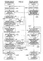
- Figure 2 is a flow chart for illustrating a power-up processing executed in the signal processing apparatus according to the first embodiment of the present invention
- Fig. 3 is a timing chart for illustrating the data transfer process when the power-up processing is executed in the signal processing apparatus according to the first embodiment of the present invention.
- the processing flow shown at the lefthand side in Fig. 2 illustrates the contents of the processing procedure executed by the microcomputer-A 10 while the processing flow shown at the righthand side in Fig. 2 illustrates the contents of the processing procedure executed by the microcomputer-B 11.
- the microcomputer-A 10 Upon power-up of the signal processing apparatus 1, the microcomputer-A 10 executes processing for initializing itself in a step s100 shown in Fig. 2 and waits for an acknowledge signal delivered from the microcomputer-B 11 in a step s105.
- the microcomputer-B 11 executes the initialize processing in a step s200 and outputs an acknowledge signal indicating a data-reception-ready state (i.e., state ready for reception of data) in a step s205.
- the microcomputer-B 11 outputs the acknowledge signal P1 by way of the GPIO signal line 70 at a time point t1.
- the microcomputer-B 11 assumes a state waiting for the reception of the microcomputer-B-dedicated main program in a step s210.
- a step s110 the microcomputer-A 10 makes decision as to whether or not the acknowledge signal has been received from the microcomputer-B 11 within a predetermined time period. Unless the acknowledge signal has been received, the microcomputer-A 10 decides that the microcomputer-B 11 suffers abnormality in operation, to thereby reset the microcomputer-B in a step s115.
- the microcomputer-A 10 executes a processing for preparing data blocks to be sent to the microcomputer-B 11 in a step s120. Thereinafter, this processing will be referred to as the sending data block preparation processing.
- the sending data block preparation processing may include, for example, clearing of an error count and setting of an initial value for the data block to be sent.
- the microcomputer-A 10 sends the data blocks of the microcomputer-B-dedicated main program data to the microcomputer-B 11. More specifically, the microcomputer-A 10 sends a data block NO. 1 DB1 by way of the serial interface 60, as can be seen in Fig. 3(A). After sending of this data block, the microcomputer-A 10 assumes the state awaiting for the acknowledge signal from the microcomputer-B 11.
- the microcomputer-B 11 set to the state ready for receiving the data in the step s210 makes decision in a step s215 as to whether or not the program data block has normally been received.
- the microcomputer-B 11 sends out the acknowledge signal in a step s220. More specifically, the microcomputer-B outputs an acknowledge signal P2 at a time point t2, as can be seen in Fig. 3(B).
- the microcomputer-A 10 makes decision as to whether or not the acknowledge signal has been received from the microcomputer-B 11 within a predetermined time period. In case the acknowledge signal P2 shown in Fig. 3(B) has been received, the microcomputer-A 10 executes the sending data block preparation processing in the step s140.
- the sending data block preparation processing includes, for example, clearing of the error count and preparation of a succeeding program data block to be sent.
- the microcomputer-A 10 increments the error count by one in a step s150 and resends the same program data block through the processing in the step s125.
- the acknowledge signal is sent from the microcomputer-B 11 after the microcomputer-A 10 has sent the data block NO. k+1 shown in Fig. 3(A) in response to the acknowledge signal Pk+1 shown in Fig. 3B, the microcomputer-A 10 sends out again the data block NO. k+1'.
- the microcomputer-A 10 checks a value of the error count in a step s155 to thereby decide whether or not the value of the error count has exceeded a predetermined value (indicating the number of times the error count has been incremented). In case the error count value has exceeded the predetermined value mentioned above, the microcomputer-A 10 resets the microcomputer-B 11 in the step s115, whereon the step s100 is resumed.
- a step s145 the microcomputer-A 10 decides whether or not sending of all the data blocks has been completed. In case this decision step s145 results in "Yes", the data transfer processing comes to an end, whereon the processing proceeds to the ordinary operation mode. Unless the data transfer has been completed yet, the microcomputer-A 10 returns to the step s125 to repeat the transfer of the program data block.
- the microcomputer-B 11 decides in a step s225 whether or not reception of all the data blocks has been completed. When the reception of all the data blocks has been completed, the microcomputer-B 11 proceeds to the ordinary operation mode.
- the program data to be sent is divided into the unitary data blocks DB of a predetermined appropriate or given size for sending, as shown in Fig. 3(A).
- the microcomputer-B for which the program data is destined sends back the acknowledge signal P1, ..., Pk+1 shown in Fig. 3(B) every time the data block transfer has successfully been completed.
- the acknowledge signal it can be conceived to send back a data block by way of the serial interface 60.
- a data block of 1-byte length at the shortest will be required as the acknowledge signal, which gives rise to a problem that a corresponding time is unwantedly required for sending back the data block as the acknowledge signal.
- the invention incarnated in the instant embodiment teaches that instead of employing the data block for the serial communication as the acknowledge signal, the polarity of the single GPIO signal line is made use of for indicating the reception normality or reception abnormality. More specifically, when the received data is normal, the polarity of the GPIO signal line is set to high level and, if otherwise, held at a low level, as can be seen in Fig. 3(B).
- the acknowledge signal P1, ..., Pk+1 indicates completion of preparation for the data reception or normality of data reception at the time point when the rising or leading edge makes appearance.
- the acknowledge signal P once assumed high level becomes low when the reception of the succeeding data block DB is started.
- the acknowledge signal of the initial state is of low level with the rising or leading edge making appearance upon completion of preparation for data reception or upon normal reception of data.
- the polarity of the acknowledge signal may be reversed such that the acknowledge signal of the initial state assumes high level with the falling or trailing edge indicating the completion of preparation for data reception or the normal data reception.
- the microcomputer-A 10 makes decision that the reception of the data block is abnormal unless the acknowledge signal has assumed the high level within a predetermined time and sends again the data block NO. k+1.
- Figure 4A shows a memory map of the flash ROM 13 employed in the signal processing apparatus according to the first embodiment of the present invention
- Fig. 4B shows a memory map of the SRAM employed in the same apparatus.
- the flash ROM memory map 400 of the flash ROM 13 incorporated in the microcomputer-A 10 is composed of a microcomputer-A-dedicated program data area 402 and a microcomputer-A-dedicated program parameter table area 403.
- Microcomputer-A-dedicated program data 404 are mapped at an address "0" of the flash ROM memory map 400.
- microcomputer-B-dedicated program data 407 are mapped, starting from the address "X" representing the microcomputer-A-dedicated program parameter table area 403.
- a run start address 405 for the program expanded on the SRAM upon power-up of the signal processing apparatus and the information concerning the data size 406.
- the microcomputer-B-dedicated program data 407 is arrayed in the memory address order in which the program is expanded on the SRAM.
- the run start address 405 shown in Fig. 4A is allocated to the leading end of the memory map 401 of the SRAM 12 connected to the microcomputer-B 11.
- the run start address 405 the data size 406 and the microcomputer-B-dedicated program data 407 are transferred to the microcomputer-B 11
- the microcomputer-B-dedicated program data 407 is expanded on the SRAM 12 by the microcomputer-B 11 on the basis of the run start address 405.
- the first data block NO. 1 shown in Fig. 3(A) contains the information concerning the start address of the main program for the microcomputer-B 11 and the size thereof.
- the program data are transferred, being carried by the data block NO. 2 and those following.
- FIG. 5 is a flow chart for illustrating a procedure of generating the flash ROM memory map 400 in the signal processing apparatus according to the first embodiment of the present invention.
- a microcomputer-A-dedicated compiler C A executes a processing for compiling a microcomputer-A-dedicated source code S A to thereby convert it into a microcomputer-A-dedicated program data file P A .
- a microcomputer-B-dedicated compiler C B executes a processing for compiling a microcomputer-B-dedicated source code S B to thereby convert it into a microcomputer-B-dedicated program data file P B .
- the microcomputer-A-dedicated program data file P A is of a data format capable of being arrayed on the flash ROM 13 incorporated in the microcomputer-A 10, while the microcomputer-B-dedicated program data file P B is of a data format capable of being arrayed on the SRAM 12 connected to the microcomputer-B.
- Data conversion software C s is designed to generate a consolidated data file D of the format capable of being arrayed on the flash ROM 13 by reading the microcomputer-A-dedicated program data file P A and the microcomputer-B-dedicated program data file P B .
- the microcomputer-A-dedicated program data files P A is arrayed in the memory address order, starting from the address "0".
- the run start address of the microcomputer-B-dedicated program data file P B and the data size thereof are arithmetically determined, whereon the run start address is disposed at the address "X" with the data size being disposed at the address succeeding to the address "X", while the microcomputer-B-dedicated program data is arrayed at the address which succeeds to the address "X".
- a single consolidated file D can be generated by consolidating or integrating the microcomputer-A-dedicated program data file P A and the microcomputer-B-dedicated program data file P B .
- Management of program version for the signal processing apparatus can be performed on a consolidated data file (D) basis.
- the program data can be embedded through a single process step.
- the flash ROM 13 may equally be connected to the microcomputer-A 10 by way of an address bus and a data bus.
- the number of constituent parts of the signal processing apparatus can be decreased by virtue of the arrangement that the program data file stored in the flash ROM incorporated in one microcomputer is transferred to other microcomputer(s) through the activation processing.
- the size of the base plate of the signal processing apparatus can be reduced when compared with the case where parallel interface is employed.
- program data of plural microcomputers can be managed as one consolidated data file, version-up of software can easily be realized.
- Figure 6 is a system block diagram showing generally and schematically a configuration of the signal processing apparatus according to the second embodiment of the present invention.
- the signal processing apparatus denoted generally by a reference numeral 810 includes therein three microcomputer-A 800, a microcomputer-B 801 and a microcomputer-X 802 and additionally SRAMs 803 and 804.
- the microcomputer-B 801 is provided with a mask ROM 806 for storing a boot program 823 which is activated upon power-up of the signal processing apparatus, while the microcomputer-X 802 is equipped with a mask ROM 807 for storing a boot program 824 which is activated when the apparatus is powered up.
- the microcomputer-A 800 and the microcomputer-B 801 are interconnected through a serial interface 850, a GPIO signal line 852 and a GPIO signal line 853.
- the microcomputer-A 800 and the microcomputer-X 802 are interconnected through a serial interface 851, a GPIO signal line 854 and a GPIO signal line 855.
- the microcomputer-A 800 stores in a flash ROM 805 the microcomputer-A-dedicated program data 820, microcomputer-B-dedicated program data 821 and microcomputer-X-dedicated program data 822 for the microcomputer-A 800, the microcomputer-B 801 and the microcomputer-X 802, respectively, which data are required for executing processings in the ordinary operation mode.
- the microcomputer-A 800 transfers the microcomputer-B-dedicated program data 821 and the microcomputer-X-dedicated program data 822 to the microcomputer-B 801 and the microcomputer-X 802 via the serial interfaces 850 and 851, respectively.
- the microcomputer-B 801 and the microcomputer-X 802 expand the program data 821 and 822 on the SRAM 803 connected via a parallel buses 860 and 861, respectively, whereupon operations of these microcomputers 801 and 802 make transition to the ordinary operation mode.
- the signal processing apparatus incorporating three or more microcomputers can be implemented in the structure similar to the apparatus incorporating two microcomputers.
- the number of parts can be reduced in the signal processing apparatus having a plurality of microcomputers and a shared ROM.
Landscapes
- Engineering & Computer Science (AREA)
- Software Systems (AREA)
- Theoretical Computer Science (AREA)
- Computer Hardware Design (AREA)
- Physics & Mathematics (AREA)
- General Engineering & Computer Science (AREA)
- General Physics & Mathematics (AREA)
- Computer Security & Cryptography (AREA)
- Multi Processors (AREA)
- Power Sources (AREA)
- Stored Programmes (AREA)
- Microcomputers (AREA)
Applications Claiming Priority (2)
| Application Number | Priority Date | Filing Date | Title |
|---|---|---|---|
| JP2001220941 | 2001-07-23 | ||
| JP2001220941A JP2003036251A (ja) | 2001-07-23 | 2001-07-23 | 信号処理装置 |
Publications (2)
| Publication Number | Publication Date |
|---|---|
| EP1280066A2 true EP1280066A2 (de) | 2003-01-29 |
| EP1280066A3 EP1280066A3 (de) | 2003-03-12 |
Family
ID=19054687
Family Applications (1)
| Application Number | Title | Priority Date | Filing Date |
|---|---|---|---|
| EP02004211A Withdrawn EP1280066A3 (de) | 2001-07-23 | 2002-02-25 | Datenverarbeitungsgerät, das eine Mehrzahl von Microrechnern und einen verteilten ROM enthält |
Country Status (3)
| Country | Link |
|---|---|
| US (1) | US20030018858A1 (de) |
| EP (1) | EP1280066A3 (de) |
| JP (1) | JP2003036251A (de) |
Cited By (2)
| Publication number | Priority date | Publication date | Assignee | Title |
|---|---|---|---|---|
| FR2923634A1 (fr) * | 2007-11-13 | 2009-05-15 | Oberthur Card Syst Sa | Carte a microprocesseur, telephone comprenant une telle carte et procede d'execution d'une commande dans une telle carte. |
| FR2923633A1 (fr) * | 2007-11-13 | 2009-05-15 | Oberthur Card Syst Sa | Carte a microprocesseur, telephone comprenant une telle carte et procede d'execution d'une commande dans une telle carte. |
Families Citing this family (5)
| Publication number | Priority date | Publication date | Assignee | Title |
|---|---|---|---|---|
| EP1651258B1 (de) * | 2003-07-30 | 2014-03-19 | Vaccine Research Institute of San Diego | Hepatitis virus kapsid-proteine als vakzine-plattformen und anwendungsverfahren dafür |
| JP4014212B2 (ja) | 2003-11-19 | 2007-11-28 | 富士通テン株式会社 | 電子制御装置 |
| US7328304B2 (en) * | 2004-02-27 | 2008-02-05 | Intel Corporation | Interface for a block addressable mass storage system |
| US7899557B2 (en) * | 2005-03-01 | 2011-03-01 | Asm Japan K.K. | Input signal analyzing system and control apparatus using same |
| US9058191B2 (en) * | 2010-03-22 | 2015-06-16 | Qualcomm Incorporated | Direct transfer of executable software image to memory allocated by target processor based on transferred image header |
Family Cites Families (14)
| Publication number | Priority date | Publication date | Assignee | Title |
|---|---|---|---|---|
| JP3310990B2 (ja) * | 1991-04-15 | 2002-08-05 | キヤノン株式会社 | 電子機器 |
| JP3461825B2 (ja) * | 1991-06-26 | 2003-10-27 | 三星電子株式会社 | マルチプロセッサ分散型初期化および自己テストシステム |
| JPH07253960A (ja) * | 1994-03-16 | 1995-10-03 | Fujitsu Ltd | マルチプロセッサシステムにおけるipl方式 |
| DE69715558T2 (de) * | 1996-10-31 | 2003-05-22 | Stmicroelectronics Ltd., Almondsbury | Mikrorechner mit Urladungsystem |
| US6493824B1 (en) * | 1999-02-19 | 2002-12-10 | Compaq Information Technologies Group, L.P. | Secure system for remotely waking a computer in a power-down state |
| US6345294B1 (en) * | 1999-04-19 | 2002-02-05 | Cisco Technology, Inc. | Methods and apparatus for remote configuration of an appliance on a network |
| US6550006B1 (en) * | 1999-07-22 | 2003-04-15 | Intel Corporation | Method and apparatus to perform a remote boot |
| US6816963B1 (en) * | 2000-01-31 | 2004-11-09 | Intel Corporation | Platform level initialization using an image generated automatically by a remote server based upon description automatically generated and transmitted thereto by a processor-based system |
| US6598159B1 (en) * | 2000-06-27 | 2003-07-22 | Intel Corporation | Option-ROM boot |
| US6622178B1 (en) * | 2000-07-07 | 2003-09-16 | International Business Machines Corporation | Method and apparatus for activating a computer system in response to a stimulus from a universal serial bus peripheral |
| US6760850B1 (en) * | 2000-07-31 | 2004-07-06 | Hewlett-Packard Development Company, L.P. | Method and apparatus executing power on self test code to enable a wakeup device for a computer system responsive to detecting an AC power source |
| US6934853B2 (en) * | 2001-01-18 | 2005-08-23 | International Business Machines Corporation | Method, system and program for sharing the ability to set configuration parameters in a network environment |
| US6732215B2 (en) * | 2001-02-05 | 2004-05-04 | Total Impact | Super scalable multiprocessor computer system |
| US6868449B1 (en) * | 2001-03-16 | 2005-03-15 | Veritas Operating Corporation | Model for cost optimization and QoS tuning in hosted computing environments |
-
2001
- 2001-07-23 JP JP2001220941A patent/JP2003036251A/ja active Pending
-
2002
- 2002-02-25 EP EP02004211A patent/EP1280066A3/de not_active Withdrawn
- 2002-02-27 US US10/083,157 patent/US20030018858A1/en not_active Abandoned
Cited By (6)
| Publication number | Priority date | Publication date | Assignee | Title |
|---|---|---|---|---|
| FR2923634A1 (fr) * | 2007-11-13 | 2009-05-15 | Oberthur Card Syst Sa | Carte a microprocesseur, telephone comprenant une telle carte et procede d'execution d'une commande dans une telle carte. |
| FR2923633A1 (fr) * | 2007-11-13 | 2009-05-15 | Oberthur Card Syst Sa | Carte a microprocesseur, telephone comprenant une telle carte et procede d'execution d'une commande dans une telle carte. |
| EP2065858A3 (de) * | 2007-11-13 | 2009-12-02 | Oberthur Technologies | Mikroprozessorkarte, eine solche Karte enthaltendes Telefon und Ausführungsverfahren eines Befehls in einer solchen Karte |
| EP2065857A3 (de) * | 2007-11-13 | 2009-12-02 | Oberthur Technologies | Mikroprozessorkarte, eine solche Karte enthaltendes Telefon und Ausführungsverfahren eines Befehls in einer solchen Karte |
| US8016203B2 (en) | 2007-11-13 | 2011-09-13 | Oberthur Technologies | Smartcard, telephone comprising such a card and method for executing a command in such a card |
| US8261996B2 (en) | 2007-11-13 | 2012-09-11 | Oberthur Technologies | Smart card, telephone comprising such a card and method for executing a command in such a card |
Also Published As
| Publication number | Publication date |
|---|---|
| US20030018858A1 (en) | 2003-01-23 |
| EP1280066A3 (de) | 2003-03-12 |
| JP2003036251A (ja) | 2003-02-07 |
Similar Documents
| Publication | Publication Date | Title |
|---|---|---|
| JP4771580B2 (ja) | プログラム制御開始方法及びファームウェア格納方法 | |
| US7765391B2 (en) | Multiprocessor system and boot-up method of slave system | |
| US6425079B1 (en) | Universal option ROM BIOS including multiple option BIOS images for multichip support and boot sequence for use therewith | |
| CN104272255B (zh) | 功能可扩展的机动车控制器和用于补充机动车控制器的功能的方法 | |
| CN106598632A (zh) | 一种光模块的固件升级方法及装置 | |
| EP2375323A1 (de) | Firmware-Bild-Aktualisierung und -Verwaltung | |
| JPH11143703A (ja) | 埋め込み型プログラマブルフラッシュメモリーを有するマイクロコントローラー | |
| CN109726163A (zh) | 一种基于spi的通信系统、方法、设备和储存介质 | |
| CN112148629B (zh) | 用于在总线上寻址集成电路的方法和对应设备 | |
| US9934120B2 (en) | Method and apparatus for updating a system on chip (SOC) image from a host computer system without using DMA | |
| EP1280066A2 (de) | Datenverarbeitungsgerät, das eine Mehrzahl von Microrechnern und einen verteilten ROM enthält | |
| CN111008101A (zh) | 一种risc-v处理器系统的调试验证平台及测试方法 | |
| US20010013091A1 (en) | Circuit arrangement and a method for creating and retrieveing replacement data | |
| ITMI20001380A1 (it) | Procedimento e dispositivo per variare il contenuto di memoria di apparecchi di comando. | |
| JP2018160207A (ja) | 車載制御装置、及び、プログラム更新ソフトウェア | |
| US6907503B2 (en) | Dual port RAM communication protocol | |
| CN110737480B (zh) | 一种串口驱动程序复用方法和装置 | |
| JP2018160208A (ja) | 車載制御装置、及び、プログラム更新ソフトウェア | |
| US20030225942A1 (en) | System and method for delivering FPGA programming | |
| JP2001125608A (ja) | プログラマブルロジックコントローラ | |
| JP2003167843A (ja) | 信号入出力装置 | |
| JP3496436B2 (ja) | プログラマブルコントローラ | |
| JP2002140206A (ja) | 待機冗長2重化制御装置及びそのアプリケーションプログラム開発装置 | |
| US20060150179A1 (en) | System for, method of registering a connection, computer readable medium and robot appliance | |
| EP1768411A1 (de) | Fernsehkamerasystem mit entsprechendem Konfigurationsverfahren |
Legal Events
| Date | Code | Title | Description |
|---|---|---|---|
| PUAI | Public reference made under article 153(3) epc to a published international application that has entered the european phase |
Free format text: ORIGINAL CODE: 0009012 |
|
| PUAL | Search report despatched |
Free format text: ORIGINAL CODE: 0009013 |
|
| AK | Designated contracting states |
Designated state(s): AT BE CH CY DE DK ES FI FR GB GR IE IT LI LU MC NL PT SE TR |
|
| AX | Request for extension of the european patent |
Extension state: AL LT LV MK RO SI |
|
| AK | Designated contracting states |
Kind code of ref document: A3 Designated state(s): AT BE CH CY DE DK ES FI FR GB GR IE IT LI LU MC NL PT SE TR Designated state(s): AT BE CH CY DE DK ES FI FR GB GR IE IT LI LU MC NL PT SE TR |
|
| AX | Request for extension of the european patent |
Extension state: AL LT LV MK RO SI |
|
| RIC1 | Information provided on ipc code assigned before grant |
Ipc: 7G 06F 9/445 B Ipc: 7G 06F 15/177 A |
|
| 17P | Request for examination filed |
Effective date: 20030711 |
|
| AKX | Designation fees paid |
Designated state(s): DE FR GB IT |
|
| 17Q | First examination report despatched |
Effective date: 20070504 |
|
| STAA | Information on the status of an ep patent application or granted ep patent |
Free format text: STATUS: THE APPLICATION IS DEEMED TO BE WITHDRAWN |
|
| 18D | Application deemed to be withdrawn |
Effective date: 20080902 |