EP1280129A2 - Dispositif d'affichage - Google Patents
Dispositif d'affichage Download PDFInfo
- Publication number
- EP1280129A2 EP1280129A2 EP02252987A EP02252987A EP1280129A2 EP 1280129 A2 EP1280129 A2 EP 1280129A2 EP 02252987 A EP02252987 A EP 02252987A EP 02252987 A EP02252987 A EP 02252987A EP 1280129 A2 EP1280129 A2 EP 1280129A2
- Authority
- EP
- European Patent Office
- Prior art keywords
- image
- signal
- image data
- section
- refresh
- Prior art date
- Legal status (The legal status is an assumption and is not a legal conclusion. Google has not performed a legal analysis and makes no representation as to the accuracy of the status listed.)
- Withdrawn
Links
Images


Classifications
-
- G—PHYSICS
- G09—EDUCATION; CRYPTOGRAPHY; DISPLAY; ADVERTISING; SEALS
- G09G—ARRANGEMENTS OR CIRCUITS FOR CONTROL OF INDICATING DEVICES USING STATIC MEANS TO PRESENT VARIABLE INFORMATION
- G09G3/00—Control arrangements or circuits, of interest only in connection with visual indicators other than cathode-ray tubes
- G09G3/20—Control arrangements or circuits, of interest only in connection with visual indicators other than cathode-ray tubes for presentation of an assembly of a number of characters, e.g. a page, by composing the assembly by combination of individual elements arranged in a matrix no fixed position being assigned to or needed to be assigned to the individual characters or partial characters
- G09G3/34—Control arrangements or circuits, of interest only in connection with visual indicators other than cathode-ray tubes for presentation of an assembly of a number of characters, e.g. a page, by composing the assembly by combination of individual elements arranged in a matrix no fixed position being assigned to or needed to be assigned to the individual characters or partial characters by control of light from an independent source
- G09G3/36—Control arrangements or circuits, of interest only in connection with visual indicators other than cathode-ray tubes for presentation of an assembly of a number of characters, e.g. a page, by composing the assembly by combination of individual elements arranged in a matrix no fixed position being assigned to or needed to be assigned to the individual characters or partial characters by control of light from an independent source using liquid crystals
- G09G3/3611—Control of matrices with row and column drivers
-
- G—PHYSICS
- G09—EDUCATION; CRYPTOGRAPHY; DISPLAY; ADVERTISING; SEALS
- G09G—ARRANGEMENTS OR CIRCUITS FOR CONTROL OF INDICATING DEVICES USING STATIC MEANS TO PRESENT VARIABLE INFORMATION
- G09G3/00—Control arrangements or circuits, of interest only in connection with visual indicators other than cathode-ray tubes
- G09G3/20—Control arrangements or circuits, of interest only in connection with visual indicators other than cathode-ray tubes for presentation of an assembly of a number of characters, e.g. a page, by composing the assembly by combination of individual elements arranged in a matrix no fixed position being assigned to or needed to be assigned to the individual characters or partial characters
- G09G3/34—Control arrangements or circuits, of interest only in connection with visual indicators other than cathode-ray tubes for presentation of an assembly of a number of characters, e.g. a page, by composing the assembly by combination of individual elements arranged in a matrix no fixed position being assigned to or needed to be assigned to the individual characters or partial characters by control of light from an independent source
- G09G3/36—Control arrangements or circuits, of interest only in connection with visual indicators other than cathode-ray tubes for presentation of an assembly of a number of characters, e.g. a page, by composing the assembly by combination of individual elements arranged in a matrix no fixed position being assigned to or needed to be assigned to the individual characters or partial characters by control of light from an independent source using liquid crystals
-
- G—PHYSICS
- G06—COMPUTING OR CALCULATING; COUNTING
- G06F—ELECTRIC DIGITAL DATA PROCESSING
- G06F3/00—Input arrangements for transferring data to be processed into a form capable of being handled by the computer; Output arrangements for transferring data from processing unit to output unit, e.g. interface arrangements
- G06F3/14—Digital output to display device ; Cooperation and interconnection of the display device with other functional units
- G06F3/1415—Digital output to display device ; Cooperation and interconnection of the display device with other functional units with means for detecting differences between the image stored in the host and the images displayed on the displays
-
- G—PHYSICS
- G09—EDUCATION; CRYPTOGRAPHY; DISPLAY; ADVERTISING; SEALS
- G09G—ARRANGEMENTS OR CIRCUITS FOR CONTROL OF INDICATING DEVICES USING STATIC MEANS TO PRESENT VARIABLE INFORMATION
- G09G3/00—Control arrangements or circuits, of interest only in connection with visual indicators other than cathode-ray tubes
- G09G3/20—Control arrangements or circuits, of interest only in connection with visual indicators other than cathode-ray tubes for presentation of an assembly of a number of characters, e.g. a page, by composing the assembly by combination of individual elements arranged in a matrix no fixed position being assigned to or needed to be assigned to the individual characters or partial characters
- G09G3/34—Control arrangements or circuits, of interest only in connection with visual indicators other than cathode-ray tubes for presentation of an assembly of a number of characters, e.g. a page, by composing the assembly by combination of individual elements arranged in a matrix no fixed position being assigned to or needed to be assigned to the individual characters or partial characters by control of light from an independent source
- G09G3/36—Control arrangements or circuits, of interest only in connection with visual indicators other than cathode-ray tubes for presentation of an assembly of a number of characters, e.g. a page, by composing the assembly by combination of individual elements arranged in a matrix no fixed position being assigned to or needed to be assigned to the individual characters or partial characters by control of light from an independent source using liquid crystals
- G09G3/3611—Control of matrices with row and column drivers
- G09G3/3648—Control of matrices with row and column drivers using an active matrix
-
- G—PHYSICS
- G09—EDUCATION; CRYPTOGRAPHY; DISPLAY; ADVERTISING; SEALS
- G09G—ARRANGEMENTS OR CIRCUITS FOR CONTROL OF INDICATING DEVICES USING STATIC MEANS TO PRESENT VARIABLE INFORMATION
- G09G2300/00—Aspects of the constitution of display devices
- G09G2300/04—Structural and physical details of display devices
- G09G2300/0404—Matrix technologies
- G09G2300/0408—Integration of the drivers onto the display substrate
-
- G—PHYSICS
- G09—EDUCATION; CRYPTOGRAPHY; DISPLAY; ADVERTISING; SEALS
- G09G—ARRANGEMENTS OR CIRCUITS FOR CONTROL OF INDICATING DEVICES USING STATIC MEANS TO PRESENT VARIABLE INFORMATION
- G09G2310/00—Command of the display device
- G09G2310/06—Details of flat display driving waveforms
-
- G—PHYSICS
- G09—EDUCATION; CRYPTOGRAPHY; DISPLAY; ADVERTISING; SEALS
- G09G—ARRANGEMENTS OR CIRCUITS FOR CONTROL OF INDICATING DEVICES USING STATIC MEANS TO PRESENT VARIABLE INFORMATION
- G09G2320/00—Control of display operating conditions
- G09G2320/02—Improving the quality of display appearance
- G09G2320/0247—Flicker reduction other than flicker reduction circuits used for single beam cathode-ray tubes
-
- G—PHYSICS
- G09—EDUCATION; CRYPTOGRAPHY; DISPLAY; ADVERTISING; SEALS
- G09G—ARRANGEMENTS OR CIRCUITS FOR CONTROL OF INDICATING DEVICES USING STATIC MEANS TO PRESENT VARIABLE INFORMATION
- G09G2320/00—Control of display operating conditions
- G09G2320/10—Special adaptations of display systems for operation with variable images
- G09G2320/103—Detection of image changes, e.g. determination of an index representative of the image change
-
- G—PHYSICS
- G09—EDUCATION; CRYPTOGRAPHY; DISPLAY; ADVERTISING; SEALS
- G09G—ARRANGEMENTS OR CIRCUITS FOR CONTROL OF INDICATING DEVICES USING STATIC MEANS TO PRESENT VARIABLE INFORMATION
- G09G2330/00—Aspects of power supply; Aspects of display protection and defect management
- G09G2330/02—Details of power systems and of start or stop of display operation
- G09G2330/021—Power management, e.g. power saving
-
- G—PHYSICS
- G09—EDUCATION; CRYPTOGRAPHY; DISPLAY; ADVERTISING; SEALS
- G09G—ARRANGEMENTS OR CIRCUITS FOR CONTROL OF INDICATING DEVICES USING STATIC MEANS TO PRESENT VARIABLE INFORMATION
- G09G2340/00—Aspects of display data processing
- G09G2340/04—Changes in size, position or resolution of an image
- G09G2340/0407—Resolution change, inclusive of the use of different resolutions for different screen areas
- G09G2340/0435—Change or adaptation of the frame rate of the video stream
Definitions
- the present invention relates to a display device which is equipped with a capacitive display element, such as a liquid crystal display element, and in particular to a display device which is capable of varying its image refresh intervals of the capacitive display element so as to reduce power consumption.
- a capacitive display element such as a liquid crystal display element
- liquid crystal display element is used in various fields as a display element for displaying images.
- the liquid crystal display element is mainly used for portable electronic devices, and for this type of devices, the major demand is to further reduce power consumption.
- the image refresh frequency (refresh rate; the number of refreshes of a displayed image in unit time) tends to increase in the liquid crystal display element which is used for a mobile phone so as to process such a large volume of information. This tendency is especially remarkable in the case of displaying a moving image.
- a display element which is made up of capacitive pixels such as a liquid crystal display element, is capable of holding a displayed state (display image) for a certain period of time once the image is refreshed by externally receiving image data of a pixel unit so that it is not required to refresh images .
- the time period of holding the displayed state differs depending on the characteristic of the capacitive display element.
- the conventional display device includes a liquid crystal controller 102, and the liquid crystal panel 103 as a display element.
- the liquid crystal controller 102 includes a display memory 104, a signal synchronization circuit 105, a display timing generation circuit 106, and a data bus 107.
- An image data signal S101 which is outputted from an external device such as a CPU is stored in the display memory 104 in the liquid crystal controller 102 via the data bus 107 of the liquid controller 102.
- the image data signal S101 which is stored in the display memory 104 is read out therefrom as an image data signal S103, and then is sent to the signal synchronization circuit 105.
- a clock signal CK101 is externally inputted to the display timing generation circuit 106 of the liquid crystal controller 102.
- the display timing generation circuit 106 according to the clock signal CK101, generates a display signal S105 for driving the liquid crystal panel 103, and a synchronization clock signal CK102 for synchronizing the image data signal S103 with the display signal S105.
- the display timing generation circuit 106 respectively outputs the display signal S105 to the liquid crystal panel 103, and the synchronization clock signal CK102 to the signal synchronization circuit 105.
- the signal synchronization circuit 105 buffers the image data signal S103 read out from the display memory 104, and outputs the image data signal S103 to the liquid crystal panel 103 as an image signal S104, according to the synchronization clock signal CK102 outputted from the display timing generation circuit 106.
- the refresh rate of the liquid crystal panel 103 corresponds to the rate of reading out image data from the display memory 104 and sending the image data to the liquid crystal panel 103 as the image data signal S103, namely, it is the value indicating how many times image signals of one frame (a screen) are sent out from the display memory 104 to the liquid crystal panel 103 in unit time.
- the image refresh frequency (refresh intervals) of the liquid crystal panel 103 can be adjusted by varying the frequency of the clock signal CK101 so as to vary the frequency of the display signal S105 which is outputted from the display timing generation circuit 106 of the liquid crystal controller 102 to the liquid crystal panel 103, and the frequency of the image signal S104 which is outputted from the signal synchronization circuit 105 to the liquid crystal panel 103.
- the image refresh frequency of the liquid crystal panel 103 is constant regardless of whether the image data signal S101 is carrying a moving image or a still image, thereby causing the following problems.
- the image refresh frequency of the liquid crystal panel 103 is commonly set to a relatively high frequency, for example, 60Hz, which is equal to a frame frequency of a video signal in the NTSC mode, to be suitable for displaying a moving image. In this case, even when a still image is displayed, the image is refreshed in the refresh frequency as high as that when displaying a moving image.
- the displayed images are not required to be refreshed at a high frequency when displaying a still image compared to the case of displaying a moving image.
- the capacitive display element such as the liquid crystal panel 103 can hold a displayed state (displayed image) for a certain period of time once the image is refreshed, and, when displaying a still image, it is not necessary to refresh the image while the displayed image is held. Therefore, in the foregoing conventional liquid crystal display device, the image refresh frequency for displaying a still image is higher than required.
- the polarity reversing frequency of scanning voltage varies depending on the image refresh frequency for the displayed image. Consequently, the power consumption of the liquid crystal panel 103 increases as the image refresh frequency for the displayed image increases, in other words, as the number of refreshes of the displayed image increases.
- the liquid crystal panel 103 consumes unnecessary power when displaying a still image, and the power consumption of the display device increases. This poses a problem especially for a battery-powered display device such as a display device used for a mobile phone whose power consumption is expressly required to be reduced.
- the number of image refreshes i.e., the image refresh frequency may be reduced by extending a period of the clock signal CK101.
- a conventional technique for lowering power consumption shown in Figure 8
- the image refresh interval may be reduced to be shorter than the frame period of a moving image; however, it may impair smoothness of the movement of the moving image.
- a liquid crystal display device capable of changing the image refresh frequency (refresh rate) based on time information (time reference) which is included in externally inputted image data, is disclosed. Further, a liquid crystal display device capable of reducing the image refresh frequency (extending the refresh interval) in the case where image data does not include a textual image, is also disclosed in this publication.
- the former invention of the foregoing publication is based on time information included in image data having a particular data structure called MPEG-4 format, and it is not applicable to image data which does not have the time information.
- This time information is included in compressed image data for indicating a timing to display a frame in MPEG-4 format which performs data compression by thinning out some frame.
- the time information is only included in image data of MPEG-4 format and not included in common image data. Accordingly, the former invention of the foregoing publication have a drawback that it is applicable only to the compressed image data of MPEG-4 format, and not applicable to other kinds of image data.
- image data commonly assumed is color signals of R, G and B which are expressed by digital signals, and each pixel has values for R, G and B.
- R, G and B are respectively expressed by 5 bits, 6 bits and 5 bits.
- the image data is moving image data which does not include a textual image, or still image data including a textual image
- the image refresh frequency becomes lower than the intended frame frequency (a frame frequency for the inputted moving image data), and smoothness of the movement of the moving image is impaired.
- the image refresh frequency becomes higher than required, thereby causing unnecessary power consumption.
- a display device includes:
- the input of the image data from the image data input section to the display control section is performed in a relatively short period of time, for example, 1/20 to 1/15 second in the case of a moving image. On the other hand it is performed only once in the case of a still image.
- the type of image data is discriminated according to a difference of input interval of the image data from the image data input section to the display control section, which differs depending on the type of the image data. Consequently, it becomes possible to discriminate the type of the image data even when time information is not included in the image data.
- refreshing an image refers to sending out an image signal of one frame to a capacitive display element, such as a liquid crystal display element, and applying a driving voltage to the pixels of the capacitive display element.
- the number of image refreshes corresponds to the number of times the image signal of one frame is sent out to the capacitive display element.
- frame refers to an image signal (image data) of one screen.
- frame frequency indicates the number of transferred frames per second when the image data is transferred
- frame period indicates a transfer period of frame when the image data is transferred.
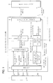
- a display device of the present embodiment includes a CPU (an image data input section, a discrimination section, and a control data generation section) 1, a liquid crystal controller 2 as a display control section, and a liquid crystal panel 3 as a capacitive display element.
- the liquid crystal controller 2 includes a display memory 4, a signal synchronization circuit (output section) 5, a display timing generation circuit 6, an image refresh demand signal generation circuit (refresh rate control section) 7, a data bus 8, and an output control circuit (output control section) 9.
- Figure 4 is a timing chart showing an example of signals used for the display device of the present embodiment.
- the CPU 1 generates image data of a moving image or a still image which is to be displayed in the liquid crystal panel 3.
- the CPU 1 generates an image data signal (image data) S1 which is made up of RGB signals for each pixel (dot) of the liquid crystal panel 3, and an address signal S11 which indicates an address (address in which the RGB signals of each pixel is written) of the display memory 4 in the liquid crystal controller 2, corresponding to each pixel.
- the CPU 1 sends out the generated image data signal S1 and the address signal S11 to the liquid crystal controller 2.
- the CPU 1 also sends out a chip selection signal S12 and a write signal S13 to the display memory 4.
- the chip selection signal S12 selects one of two memory chips in the display memory 4 for writing data.
- the write signal S13 controls ON/OFF of the writing operation of the image data signal S1 to the display memory 4.
- the CPU 1 activates these chip selection signal S12 and write signal S13 when the image data signal S1 and the address signal S11 are sent to the display memory 4 (the CPU 1 deactivates these signals in other cases).
- the image data signal S1 and the address signal S11 are generated and sent to the display memory 4 one frame at a time.
- the CPU 1 sends the image data signal S1 to the display memory 4 at the same time intervals the image data signal S1 is generated by the CPU 1. Therefore, the time intervals for sending out the image data signal S1 differs depending on whether the image data signal S1 is a still image or a moving image.
- the CPU 1 generates only one image data signal S1 for a single still image. Accordingly, for example, in the case of displaying a plurality of still images by switching them as in the case of a slide show, the image data signal S1 is sent out to the display memory 4 at the time intervals the still images are switched, in other words, at the time intervals the image data signal S1 of the still image is generated.
- the time intervals for switching still images are longer than the frame period of a moving image. Normally, the time intervals for switching still images are not less than 1/10 second. Therefore, the time intervals for sending out the image data signal S1 of the still image from the CPU 1 to the display memory 4 are also longer than the frame period of a moving image, i.e., normally at or longer than 1/10 second.
- the CPU 1 generates the image data signal S1 of a moving image one frame at a time at a constant period corresponding to the frame frequency of the generated image data signal S1.
- the image data signal S1 of a moving image of 15 to 20 frames per second is generated one frame at a time at the intervals of 1/20 second to 1/15 second (15 times to 20 times per second).
- the image data signal S1 of a moving image is sent out from the CPU 1 to the display memory 4 at constant intervals corresponding to the frame frequency of the image data signal S1, for example, at the intervals of 1/20 second to 1/15 second (15 times to 20 times per second) in the case of an image data signal S1 of a moving image of 15 to 20 frames per second.
- the time intervals for sending out the image data signal S1 from the CPU 1 to the display memory 4 become shorter than the case where the image data signal S1 is a still image.
- the time intervals for sending out the image data signal S1 from the CPU 1 to the display memory 4 are 1/5 second in the case where the image data signal S1 is a moving image.
- the time intervals for sending out the image data signal S1 from the CPU 1 to the display memory 4 are 1/15 second in the case where the image data signal S1 is a still image.
- Figure 3 is a diagram showing the number of frames in unit time, in the image data signal S1, image signal S4, and image signal S7. In the figure, a quadrilateral indicates one frame.
- the CPU 1 discriminates whether the image data signal S1 is a still image or a moving image based on the duration of the time intervals for sending out the image data signal S1 from the CPU 1 to the display memory 4. More specifically, the CPU 1 judges that the image data signal S1 is a still image, when the time intervals for sending out the image data signal S1 from the CPU 1 to the display memory 4 are at or longer than a certain time period, and judges that the image data signal S1 is a moving image, when the time intervals for sending out the image data signal S1 from the CPU 1 to the display memory 4 are shorter than this time period.
- whether or not the image data signal S1 is a still image or a moving image is decided according to whether the time intervals for sending out the image data signal S1 from the CPU 1 to the display memory 4 are at or longer than or shorter than 1/12 second.
- the CPU 1 determines the number of image refresh n and the number of image thin-out (the number of non-refreshes) m, according to the result of discrimination, namely, according to whether the image data signal S1 is a still image or a moving image.
- the number of image refreshes n is the number of times an image is refreshed during a time period in which the image signal S4 of one frame (n + m) is outputted.
- the number of image thin-out m is the number of times the image signal S4 is thinned out during a time period in which the image signal S4 of one frame (n + m) is outputted, in other words, the number of (n + m) frame periods of the image signal S4 in which the image is not refreshed.
- control data control data
- the CPU 1 generates a control data signal (control data) S2 which includes a data signal (an image refresh rate data signal S9 described later) indicating the number of image refreshes n, and a data signal (an image thin-out rate data signal S10 described later) indicating the number of image thin-out m.
- the CPU 1 outputs the control data signal S2 to the image refresh demand signal generation circuit 7, with the image data signal S1.
- the image data signal S1 outputted from the CPU 1 is stored in the display memory 4 via the data bus 8.
- the image data signal S1 is written on a memory chip in the display memory 4 which is specified by the chip selection signal S12, when the chip selection signal S12 and the write signal S13 are activated (when the image data signal S1 and the address signal S11 are sent out from the CPU 1).
- the image data signal S1 is written on an address of the display memory 4 specified by the address signal S11, with respect to each pixel signal (RGB signal corresponding to a color pixel).
- the image data signal S1 is written (buffered) to the display memory 4 of the liquid controller 2 at the same time intervals at which the image data signal S1 is sent from the CPU 1 to the display memory 4. Accordingly, the refresh interval of the display memory 4 is relatively long, for example, at or longer than 1 second in the case where the image data signal S1 is a still image, and the refresh interval of the display memory 4 is relatively short, for example, 1/20 second to 1/15 second in the case where the image data signal S1 is a moving image.
- control signal S2 outputted from the CPU 1 is stored in the image refresh demand signal generation circuit 7 via the data bus 8.
- the image data signal S1 stored in the display memory 4 is read out as the image data signal (image data) S3 from the display memory 4, then is sent out to the signal synchronization circuit 5.
- a clock signal CK1 shown in Figure 4 is externally inputted to the display timing generation circuit 6 of the liquid crystal controller 2.
- the display timing generation circuit 6 generates a display signal S15 for driving the liquid crystal panel 3, according to the clock signal CK1.
- the display signal S15 is a timing signal which indicates a timing for outputting each frame of the image signal S4, so as to capture the image signal S4 in the liquid crystal panel 3 one frame at a time.
- the display signal S15 is always outputted per one frame (screen) period of the image signal S4 (described later).
- the display signal S15 is a periodic signal having the same period (a period of 1/60 second) as a frame period (image refresh frequency) of a common moving image (a video signal in the NTSC mode).
- the display timing generation circuit 6 generates a synchronization clock signal CK2 for synchronizing the image data signal S3 with the display signal S5.
- the display timing generation circuit 6 respectively outputs the display signal S15 to the output control circuit 9, and the synchronization clock signal CK2 to the signal synchronization circuit 5, at the same period (a period of 1/60 second) as a frame period (image refresh frequency) of a common moving image.
- the clock signal CK1 and the synchronization clock signal CK2 are identical, and the both are system clocks for driving the liquid crystal controller 2.
- the display timing generation circuit 6 outputs a frame end signal S8 shown in Figure 4 to the image refresh demand signal generation circuit 7, at the end of each frame of the display signal S15 (at the end of each frame of the image signal S4).
- the frame end signal S8 is a signal for informing the end of a frame (screen) of the image signal S4, and is outputted when the last pixel signal of the image signal S4 of a frame (screen) is sent out to the output control circuit 9.
- the signal synchronization circuit 5 buffers the image data signal S3 read out from the display memory 4, and outputs the image data signal S3 according to the synchronization clock signal CK2 to the output control circuit 9 as the image signal S4 which has the same frame period (a period of 1/60 second) as the a frame period of a common moving image (an video signal in the NTSC mode) shown in Figure 4, .
- the image signal S4 is outputted in phase with the display signal S5.
- the image data signal S1, the image data signal S3, and the image signal S4 are data of R, G, B corresponding to each pixel of the liquid crystal panel 3, and they indicates the same data but are asynchronous.
- the image refresh demand signal generation circuit 7 generates an image refresh demand signal S6 from the control data signal S2 inputted from the CPU 1, and the frame end signal S8 outputted from the display timing generation circuit 6, and then outputs the image refresh demand signal S6 to the output control circuit 9.
- the image refresh demand signal S6 is a signal which is active during the image refresh period, and is inactive during the image thin-out period (non image refresh period).
- the output control circuit 9 outputs the image signal S4 and the display signal S15 only when the image refresh demand signal S6 inputted from the image refresh demand signal generation circuit 7 is active (i.e., in the image refresh period).
- the image signal S7 outputted from the output control circuit 9 becomes a signal with an image thin-out period which corresponds to the image thin-out period of the image signal S4.
- the display signal S5 outputted from the output control circuit 9 becomes a signal with an image thin-out period which corresponds to the image thin-out period of the display signal S15. Consequently, as shown in Figure 4, the display signal S5 is active during the image refresh period, and is inactive during the image thin-out period.
- a driving voltage according to the image signal S7 is applied to pixels during the period in which the display signal S5 is active (image refresh period). Meanwhile, the driving voltage is not applied to pixels during the period in which the display signal S5 is inactive (image thin-out period).
- image refresh period the driving voltage is not applied to pixels during the period in which the display signal S5 is inactive (image thin-out period).
- the image refresh demand signal generation circuit 7 includes a refresh rate setting register 11, a thin-out rate setting register 12, and an image refresh demand judgment circuit (timing instructing section) 13.
- a control data signal S2 which includes a data signal (an image refresh rate data signal S9) indicating the number of image refreshes n, and a data signal (an image thin-out rate data signal S10) indicating the number of image thin-out m, is inputted from the CPU 1 to the image refresh demand signal generation circuit 7 via the data bus 8.
- the image refresh rate data signal S9 and the image thin-out rate data signal S10 which are included in the control data signal S2, are respectively stored (set) in the image refresh rate setting register 11 and the thin-out rate setting register 12.
- These data signals S9 and S10 are stored (set) in the registers 11 and 12, for example, by latching the signals with a system clock, or, by latching the signals at the edge of a write clock which has been separately provided.
- the image refresh demand judgment circuit 13 determines the number of image refreshes n and the number of image thin-out m according to the values of the image refresh rate data signal S9 and the image thin-out rate data signal S10 (the values set by the image refresh rate setting register 11 and the thin-out rate setting register 12), respectively.
- the image refresh demand judgment circuit 13 has a counter (not shown) for counting the frame end signal S8, and the image refresh demand judgment circuit 13 outputs the image refresh demand signal S6 until the value of the counter matches the number of image refreshes n.
- the image refresh demand judgment circuit 13 deactivate the image refresh demand signal S6 while resetting the counter, and then starts counting the frame end signal S8 again.
- the image refresh demand signal S6 stays deactivated until the value of the counter matches the number of image thin-out m.
- the image refresh demand judgment circuit 13 resets the counter, and then activates the image refresh demand signal S6.
- the image refresh demand judgment circuit 13 repeats these procedures so as to periodically activate and deactivate the image refresh demand signal S6.
- the active period of the image refresh demand signal S6 is equal to n times the period of the frame end signal S8, in other words, m times the frame period of the image signal S4.
- the inactive period of the image refresh demand signal S6 equal to m times the period of the frame end signal S8, in other words, n times the frame period of the image signal S4.
- the liquid crystal panel 3 alternately performs image refresh for the time period equals to n times the frame period (1/60 second) of the image signal S4, and image non-refresh for the time period equals to m times the frame period (1/60 second) of the image signal S4.
- the image refresh demand judgment circuit 13 has a mask function which uses an image refresh demand signal which is always active, and masks (deactivates) a portion of the image refresh demand signal for a time period which corresponds to the image non-refresh period, so as to generate the image refresh demand signal S6 which is active only in part.
- Figure 3 is a timing chart showing the frame intervals of the image data signal S1, the image signal S4, and the image signal S7, when displaying a still image and displaying a moving image.
- the number of refreshes of the display memory (the number of times the image data signal S1 of one frame is sent) is one, when displaying a still image.
- n and m when displaying a still image and n and m when displaying moving image are set so that n/m when displaying a still image is smaller than n/m when displaying a moving image.
- the number of image refreshes in unit time when displaying a still image is smaller than the number of image refreshes in unit time when displaying a moving image.
- the number of image refreshes in unit time when displaying a moving image is 30, whereas the number of image refreshes in unit time when displaying a still image is 20. This prevents extra power consumption due to unnecessary image refreshes when displaying a still image, thereby reducing power consumption.
- the liquid crystal panel 3 it is desirable to make the image refresh intervals of the liquid crystal panel 3 when displaying a still image as long as possible to reduce power consumption; however, there is an upper time limit that the liquid crystal panel 3 can hold the image. Namely, it is required to perform the image refresh of the liquid crystal panel 3 according to the image holding characteristics (a rate at which charge escapes) of the liquid crystal panel 3. For example, in order to keep displaying a single still image, it is required to perform the image refresh (applying a driving voltage) by repeatedly sending out the same image signal to the liquid crystal panel 3 at the intervals longer than a certain time period (image holding time).
- the upper limit of the image refresh should be determined according to the image holding characteristic of the liquid crystal panel 3 so that it becomes shorter than the image holding time of the liquid crystal panel 3.
- the image holding time is about 1/20 second.
- a liquid crystal panel 3 which is currently under development holds promise of improving the image holding time to about 1/5 second.
- the image refresh rate when displaying a still image becomes three times the frame period of the image signal S4, i.e., about 1/20 second.
- the image signal S4 of a still image can be thinned out to 1/3, and the image refresh rate when displaying a still image becomes 20 times per second.
- the image refresh interval when displaying a still image becomes twelve times the frame period of the image signal S4, i.e., about 1/5 second.
- the image signal S4 of a still image can be thinned out to 1/12, and the image refresh rate when displaying a still image becomes 5 times per second.
- the image refresh intervals of the liquid crystal panel 3 when displaying a moving image are desirable to make as long as possible to reduce power consumption; however, for a smooth display of the moving image, the intervals should be more desirably shorter than the frame period of the image data signal S1 which is sent out from the CPU 1 to the display memory 4.
- the image refresh interval when displaying a moving image is required to be no longer than 1/20 to 1/15 second, when the frame period of the image data signal S1 which is sent out from the CPU 1 to the display memory 4 is 1/20 to 1/15 second (15 to 20 frames per second).
- the image refresh interval when displaying a moving image becomes three times the frame period of the image signal S4, i.e., about 1/20 second.
- the image signal S4 of a moving image can be thinned out to 1/3, and the image refresh rate when displaying a moving image becomes 20 times per second.
- n should be not less than 2.
- the number of image refreshes n is set to 2 or 3
- the number of image thin-out m is set to about 5.
- the display device of the present embodiment does not change the image refresh frequency of the liquid crystal panel 103 by changing the frequencies of the image signal S104 and the display signal S105 which are outputted from the liquid crystal controller 102 to the liquid crystal panel 103.
- the display device of the present embodiment can change the image refresh frequency of the liquid crystal panel 3 by the CPU 1 in a structure of the liquid crystal controller 2 including:
- the CPU 1 has a function for discriminating whether the image data signal S1 is a moving image or a still image.
- this function can be included in the liquid crystal controller 2. Namely, it is possible to discriminate whether the image data signal S1 is a moving image or a still image by the liquid crystal controller 2 based on transfer intervals (time intervals for refreshing images) of the image data signal S1 when it is transferred from the CPU 1 to the display memory 4.
- a liquid crystal display of the present embodiment has the same arrangement as that of the first embodiment, except for an image refresh demand signal generation circuit 17 which is provided as an image refresh rate control section, instead of the image refresh demand signal generation circuit 7.
- the image refresh demand signal generation circuit 17 further includes a mode switching signal generation circuit (operation control section) 14, and an ON/OFF switch 15 (operation control section) for switching on/off the operation of the image refresh demand judgment circuit 13, in addition to the functions of the image refresh demand signal generation circuit 7.
- the mode switching signal generation circuit 14 switches off the ON/OFF switch 15 when the ratio (m/n) between the number of image thin-out m and the number of image refreshes n is at or smaller than a predetermined value, and switches on the ON/OFF switch 15 when the ratio (m/n) between the number of image thin-out m and the number of image refreshes n is greater than the predetermined value, based on at least either one of the number of image thin-out m set by the image thin-out rate data signal S10, or the number of image refreshes n set by an image refresh rate data signal S9.
- the image refresh demand judgment circuit 13 stops operating when the ratio (m/n) between the number of image thin-out m and the number of image refreshes n is at or smaller than the predetermined value, and the image refresh demand judgment circuit 13 starts operating when the ratio (m/n) between the number of image thin-out m and the number of image refreshes n is greater than the predetermined value.
- the mode switching signal generation circuit 14 stops the operation of the image refresh demand judgment circuit 13 when the ratio (m/n) between the number of image thin-out m and the number of image refreshes n is 0, and starts the operation of the image refresh demand judgment circuit 13 when the ratio (m/n) between the number of image thin-out m and the number of image refreshes n is not 0.
- the mode switching signal generation circuit 14 controls the operation of the image refresh demand judgment circuit 13 based on only the number of image thin-out m set by the refresh rate setting register 11.
- the liquid crystal controller 2 stops the operation of the image refresh demand judgment circuit 13 when the ratio (m/n) between the number of image thin-out m and the number of image refreshes n is at or smaller than a predetermined value, and outputs the image signal S4 directly to the liquid crystal panel 3 so as to operate in a mode (normal refresh mode) in which images of the liquid crystal panel 3 are refreshed at normal refresh intervals (1/60 second).
- the liquid crystal controller 2 starts the operation of the image refresh demand judgment circuit 13 when the ratio (m/n) between the number of image thin-out m and the number of image refreshes n is greater than the predetermined value, and thins out the image signal S4, so as to operate in a mode (refresh interval thin-out mode) in which images of the liquid crystal panel 3 are refreshed at refresh intervals which are longer than the normal refresh intervals.
- Figure 6 is a timing chart of the normal refresh mode and the refresh interval thin-out mode, which are switched between still image display and moving image display.
- the number of image thin-out m is set to 0, and the number of image refreshes n is set to 1 when displaying the moving image.
- the number of image thin-out m is set to 4, and the number of image refreshes n is set to 2 when displaying the still image.
- the mode switching signal generation circuit 14 stops the operation of the image refresh demand judgment circuit 13, and switches the mode to the normal refresh mode.
- the image refresh demand judgment circuit 13 has the function (masking function) of masking the image non-refresh period of an image refresh demand signal which is always active. Therefore, this mask function does not work while the operation of the image refresh demand judgment circuit 13 is stopped, and the image refresh demand constantly arises. Namely, the image refresh demand signal S6 is always active while the operation of the image refresh demand judgment circuit 13 is stopped. Consequently, the image signal S4 is constantly outputted in the normal refresh mode.
- the mode switching signal generation circuit 14 starts the operation of the image refresh demand judgment circuit 13, and switches the mode to the refresh interval thin-out mode.
- the image refresh demand judgment circuit 13 masks the image non-refresh period of an image refresh demand signal which is always active, as with the first embodiment.
- the value is externally set by using the ON/OFF switch 15 as a register; however, it can also be set by the mode switching signal generation circuit 14 which controls the ON/OFF switch 15 according to the value of the thin-out rate setting register 12. In this way, an extra register will not be required.
- the operation of the image refresh demand judgment circuit 13 is controlled based on only the number of image thin-out m; however, provided that the operation of the image refresh demand judgment circuit 13 according to a change of the ratio between the number of image thin-out m and the number of image refreshes n can be controlled, the operation of the image refresh demand judgment circuit 13 may be controlled based on other information. Namely, the operation of the image refresh demand judgment circuit 13 can be controlled based on only the number of image refreshes n, or based on both the number of image thin-out m and the number of image refreshes n.
- a display device of the present invention preferably includes:
- the output control section thins out the image signal of certain time intervals (for example, an image signal of a moving image having a frame period of 1/60 second as with a common television video signal), and varies the ratio (number of thin-out/number of transfers) for thinning out the image signal varies depending on the type of the image data.
- the transfer timing of the image signal is varied, it becomes possible to freely control the image refresh timing compared with the case of changing the frequency of the transferred image signal.
- the output section, the output control section, and the timing instructing section in the foregoing arrangement can be realized by a liquid crystal controller including a memory for holding image data and a circuit section for setting a rate of sending out the image data (image refresh rate) from the memory to the capacitive display element.
- the refresh rate control section further includes an operation control section which stops operation of the timing instructing section when the integer ratio m/n is not more than a predetermined value, according to at least either the integral value m or n, so as to directly transfer an image signal outputted from the output section to the capacitive display element.
- the refresh rate control section further includes an operation control section which switches to a mode in which the operation of the timing instructing section is stopped and images are refreshed at normal refresh intervals according to the image signal outputted from the output section, from a mode in which images are refreshed at a slower image refresh rate by thinning out the image signal outputted from the output section according to at least either one of the integral values m and n, when the integral ratio m/n is not more than a predetermined value.
- the display device of the present invention when the integer value m/n is small, in other words, the ratio to thin out the image signal is low, the reduction of power consumption by thinning out the image signal becomes relatively low. Consequently, the power consumed by operating of the timing instructing section will be larger than the reduction, and power consumption of the entire display device will possibly increase, opposing the intention.
- the operation control section stops the operation of the timing instructing section, and directly transfers the image signal outputted from the output section to the capacitive display element when the ratio for thinning out the image signal is small as in the case above. This makes it possible to prevent an increase of power consumption of the entire device caused by the operation of the timing instructing section, thereby further reducing power consumption of the entire device.
- the display control section includes a storage section for storing the image data so as to individually and arbitrarily control input intervals and output intervals of the image data.
- the refresh rate control section sets the image refresh rate in the capacitive display element higher than the number of frames of the image data, for a smooth display of a moving image.
- the refresh rate control section sets the image refresh rate as low as possible within a range that the capacitive display element can hold the display image, when the image data is recognized as a still image. Namely, it is preferable that the image refresh interval when the image data is a still image is set to the highest value at which the capacitive display element can hold the display image without problems, according to the image holding characteristics (data holding characteristics) of the capacitive display element.
- the refresh rate control section refreshes images one after another for plural times in displaying both a moving image and a still image so as to suppress flicker of the displayed image of the display element. Accordingly, in the arrangement including the control data generation section which generates control data indicating the integer values m and n, it is preferable that n is not less than 2 and the output control section thins out the image data m times and transfers the image data n times alternately.
- the capacitive display element is not limited to a liquid crystal display element. Any display elements (capacitive display elements), made up of pixels having a capacitive load, and capable of holding a displayed image for a certain period of time without applying a voltage to the pixels, can be adopted.
Landscapes
- Engineering & Computer Science (AREA)
- Theoretical Computer Science (AREA)
- Physics & Mathematics (AREA)
- General Physics & Mathematics (AREA)
- Chemical & Material Sciences (AREA)
- Crystallography & Structural Chemistry (AREA)
- Computer Hardware Design (AREA)
- Human Computer Interaction (AREA)
- General Engineering & Computer Science (AREA)
- Control Of Indicators Other Than Cathode Ray Tubes (AREA)
- Liquid Crystal Display Device Control (AREA)
Applications Claiming Priority (2)
| Application Number | Priority Date | Filing Date | Title |
|---|---|---|---|
| JP2001228567 | 2001-07-27 | ||
| JP2001228567A JP3749147B2 (ja) | 2001-07-27 | 2001-07-27 | 表示装置 |
Publications (2)
| Publication Number | Publication Date |
|---|---|
| EP1280129A2 true EP1280129A2 (fr) | 2003-01-29 |
| EP1280129A3 EP1280129A3 (fr) | 2004-12-08 |
Family
ID=19061060
Family Applications (1)
| Application Number | Title | Priority Date | Filing Date |
|---|---|---|---|
| EP02252987A Withdrawn EP1280129A3 (fr) | 2001-07-27 | 2002-04-26 | Dispositif d'affichage |
Country Status (6)
| Country | Link |
|---|---|
| US (1) | US7123246B2 (fr) |
| EP (1) | EP1280129A3 (fr) |
| JP (1) | JP3749147B2 (fr) |
| KR (1) | KR100445285B1 (fr) |
| CN (1) | CN1287341C (fr) |
| TW (1) | TWI233072B (fr) |
Cited By (28)
| Publication number | Priority date | Publication date | Assignee | Title |
|---|---|---|---|---|
| WO2008026070A3 (fr) * | 2006-08-31 | 2008-05-02 | Ati Technologies Ulc | Réglage de fréquences d'images dynamique |
| EP1640951A3 (fr) * | 2004-09-27 | 2008-07-30 | Idc, Llc | Procede de regulation d'une frequence de rafraichissement d'un affichage bistable, par exemple un telephone portable |
| US7499208B2 (en) | 2004-08-27 | 2009-03-03 | Udc, Llc | Current mode display driver circuit realization feature |
| US7515147B2 (en) | 2004-08-27 | 2009-04-07 | Idc, Llc | Staggered column drive circuit systems and methods |
| US7560299B2 (en) | 2004-08-27 | 2009-07-14 | Idc, Llc | Systems and methods of actuating MEMS display elements |
| GB2458958A (en) * | 2008-04-04 | 2009-10-07 | Sony Corp | LCD driving circuit for reducing refresh rate if image data is prone to flicker |
| EP2172923A3 (fr) * | 2004-08-10 | 2010-04-21 | Sony Corporation | Appareil et procédé d'affichage |
| US7920136B2 (en) | 2005-05-05 | 2011-04-05 | Qualcomm Mems Technologies, Inc. | System and method of driving a MEMS display device |
| US7948457B2 (en) | 2005-05-05 | 2011-05-24 | Qualcomm Mems Technologies, Inc. | Systems and methods of actuating MEMS display elements |
| US7957589B2 (en) | 2007-01-25 | 2011-06-07 | Qualcomm Mems Technologies, Inc. | Arbitrary power function using logarithm lookup table |
| US8049713B2 (en) | 2006-04-24 | 2011-11-01 | Qualcomm Mems Technologies, Inc. | Power consumption optimized display update |
| US8085461B2 (en) | 2004-09-27 | 2011-12-27 | Qualcomm Mems Technologies, Inc. | Systems and methods of actuating MEMS display elements |
| US8233014B2 (en) | 2009-09-15 | 2012-07-31 | Chunghwa Picture Tubes, Ltd. | Color sequential display and power saving method thereof |
| US8243014B2 (en) | 2004-09-27 | 2012-08-14 | Qualcomm Mems Technologies, Inc. | Method and system for reducing power consumption in a display |
| US8310441B2 (en) | 2004-09-27 | 2012-11-13 | Qualcomm Mems Technologies, Inc. | Method and system for writing data to MEMS display elements |
| US8405649B2 (en) | 2009-03-27 | 2013-03-26 | Qualcomm Mems Technologies, Inc. | Low voltage driver scheme for interferometric modulators |
| CN103238177A (zh) * | 2011-09-06 | 2013-08-07 | 夏普株式会社 | 显示装置及其驱动方法 |
| US8514169B2 (en) | 2004-09-27 | 2013-08-20 | Qualcomm Mems Technologies, Inc. | Apparatus and system for writing data to electromechanical display elements |
| CN103744632A (zh) * | 2013-11-28 | 2014-04-23 | 苏州长风航空电子有限公司 | 一种基于NiosⅡ的低成本机载显示器图形生成装置及其方法 |
| EP2652730A4 (fr) * | 2010-12-13 | 2014-06-18 | Ati Technologies Ulc | Procédé et appareil fournissant une indication de trame statique |
| US8878825B2 (en) | 2004-09-27 | 2014-11-04 | Qualcomm Mems Technologies, Inc. | System and method for providing a variable refresh rate of an interferometric modulator display |
| WO2015160297A1 (fr) * | 2014-04-17 | 2015-10-22 | Pricer Ab | Procédé de balayage pour dispositif d'affichage |
| EP2894625A4 (fr) * | 2012-09-07 | 2016-06-08 | Sharp Kk | Dispositif de commande de sortie de données d'image, dispositif d'affichage, programme et support d'enregistrement associé |
| US9703423B2 (en) | 2010-01-20 | 2017-07-11 | Semiconductor Energy Laboratory Co., Ltd. | Electronic device and electronic system |
| US9959822B2 (en) | 2009-10-16 | 2018-05-01 | Semiconductor Energy Laboratory Co., Ltd. | Liquid crystal display device and electronic device including the liquid crystal display device |
| US10013087B2 (en) | 2010-04-28 | 2018-07-03 | Semiconductor Energy Laboratory Co., Ltd. | Semiconductor display device and driving method the same |
| US10255868B2 (en) | 2009-12-25 | 2019-04-09 | Semiconductor Energy Laboratory Co., Ltd. | Method for driving liquid crystal display device |
| US10847116B2 (en) | 2009-11-30 | 2020-11-24 | Semiconductor Energy Laboratory Co., Ltd. | Reducing pixel refresh rate for still images using oxide transistors |
Families Citing this family (93)
| Publication number | Priority date | Publication date | Assignee | Title |
|---|---|---|---|---|
| KR100429880B1 (ko) * | 2001-09-25 | 2004-05-03 | 삼성전자주식회사 | Lcd 프레임 비율 제어 회로 및 방법과 lcd 시스템 |
| JP2004088750A (ja) * | 2002-06-28 | 2004-03-18 | Rohm Co Ltd | 携帯通信機器 |
| KR20040013609A (ko) * | 2002-08-07 | 2004-02-14 | 삼성전자주식회사 | 휴대용 컴퓨터 및 그 제어방법 |
| JP4082155B2 (ja) * | 2002-09-30 | 2008-04-30 | 株式会社日立製作所 | 携帯端末 |
| BR0306516A (pt) * | 2002-10-01 | 2005-01-25 | Sony Corp | Aparelho, método e programa para um aparelho para processamento de informação, e, meio de gravação |
| US7119803B2 (en) * | 2002-12-30 | 2006-10-10 | Intel Corporation | Method, apparatus and article for display unit power management |
| JP2004254993A (ja) * | 2003-02-27 | 2004-09-16 | Daiman:Kk | 遊技機 |
| JP3907609B2 (ja) * | 2003-04-30 | 2007-04-18 | 株式会社ソニー・コンピュータエンタテインメント | ゲーム実行方法、ゲーム機、通信方法および通信装置 |
| CN100350809C (zh) * | 2003-12-05 | 2007-11-21 | 联发科技股份有限公司 | 便携式电子装置及其电源管理方法 |
| KR100965597B1 (ko) * | 2003-12-29 | 2010-06-23 | 엘지디스플레이 주식회사 | 액정표시장치의 구동방법 및 구동장치 |
| JP4864460B2 (ja) * | 2004-02-04 | 2012-02-01 | パナソニック株式会社 | 再生装置、再生方法およびプログラム |
| KR100619833B1 (ko) * | 2004-03-05 | 2006-09-13 | 엘지전자 주식회사 | 이동 통신 단말기의 화면 업데이트 방법 |
| CN1860521A (zh) * | 2004-08-10 | 2006-11-08 | 索尼株式会社 | 显示设备和方法 |
| US7551159B2 (en) * | 2004-08-27 | 2009-06-23 | Idc, Llc | System and method of sensing actuation and release voltages of an interferometric modulator |
| US7889163B2 (en) | 2004-08-27 | 2011-02-15 | Qualcomm Mems Technologies, Inc. | Drive method for MEMS devices |
| US7602375B2 (en) | 2004-09-27 | 2009-10-13 | Idc, Llc | Method and system for writing data to MEMS display elements |
| US7675669B2 (en) * | 2004-09-27 | 2010-03-09 | Qualcomm Mems Technologies, Inc. | Method and system for driving interferometric modulators |
| US20060066596A1 (en) * | 2004-09-27 | 2006-03-30 | Sampsell Jeffrey B | System and method of transmitting video data |
| US20060176241A1 (en) * | 2004-09-27 | 2006-08-10 | Sampsell Jeffrey B | System and method of transmitting video data |
| US7920135B2 (en) * | 2004-09-27 | 2011-04-05 | Qualcomm Mems Technologies, Inc. | Method and system for driving a bi-stable display |
| JP2006203333A (ja) * | 2005-01-18 | 2006-08-03 | Canon Inc | 双方向リモートコントロールユニット |
| JP3863904B1 (ja) * | 2005-03-30 | 2006-12-27 | シャープ株式会社 | 液晶表示装置 |
| EP1717783B1 (fr) * | 2005-04-28 | 2015-06-03 | Semiconductor Energy Laboratory Co., Ltd. | Circuit fermé de données, procédé de commande du circuit fermé et dispositif d'affichage |
| US20070126673A1 (en) * | 2005-12-07 | 2007-06-07 | Kostadin Djordjev | Method and system for writing data to MEMS display elements |
| US7414230B2 (en) * | 2005-12-08 | 2008-08-19 | Graphic Packaging International, Inc. | Package with removable portion |
| US8391630B2 (en) * | 2005-12-22 | 2013-03-05 | Qualcomm Mems Technologies, Inc. | System and method for power reduction when decompressing video streams for interferometric modulator displays |
| CN100412776C (zh) * | 2005-12-22 | 2008-08-20 | 佛山市顺德区顺达电脑厂有限公司 | 便携式装置触控屏幕灵敏度的调整方法 |
| US8194056B2 (en) * | 2006-02-09 | 2012-06-05 | Qualcomm Mems Technologies Inc. | Method and system for writing data to MEMS display elements |
| US7702192B2 (en) * | 2006-06-21 | 2010-04-20 | Qualcomm Mems Technologies, Inc. | Systems and methods for driving MEMS display |
| US7898535B2 (en) * | 2006-10-31 | 2011-03-01 | Dell Products, Lp | System and method for providing dynamic refresh rates for displays |
| US8040334B2 (en) * | 2006-12-29 | 2011-10-18 | 02Micro International Limited | Method of driving display device |
| CN100543821C (zh) * | 2007-04-04 | 2009-09-23 | 友达光电股份有限公司 | 驱动电路、显示装置及用以调整画面更新率的方法 |
| KR101222987B1 (ko) | 2007-05-11 | 2013-01-17 | 엘지디스플레이 주식회사 | 액정표시장치와 그 구동방법 |
| CN101681211A (zh) | 2007-05-21 | 2010-03-24 | 伊英克公司 | 用于驱动视频电光显示器的方法 |
| US20090015579A1 (en) * | 2007-07-12 | 2009-01-15 | Qualcomm Incorporated | Mechanical relaxation tracking and responding in a mems driver |
| JP2009025677A (ja) * | 2007-07-23 | 2009-02-05 | Renesas Technology Corp | 液晶パネルの駆動制御回路および半導体装置 |
| US8115726B2 (en) * | 2007-10-26 | 2012-02-14 | Hewlett-Packard Development Company, L.P. | Liquid crystal display image presentation |
| TW200949822A (en) * | 2007-11-26 | 2009-12-01 | Tpo Displays Corp | Display system and method for reducing power consumption of same |
| KR20100119556A (ko) | 2008-02-11 | 2010-11-09 | 퀄컴 엠이엠스 테크놀로지스, 인크. | Mems 기반 디스플레이용의 전기적 구동 변수의 전기적 측정을 위한 방법 및 장치 |
| BRPI0908803A2 (pt) * | 2008-02-11 | 2015-07-21 | Qualcomm Mems Technologie Inc | Dispositivo e método de sensoreamento, mensuração ou caracterização de elementos de tela integrados com o esquema de drive de tela |
| JP5185697B2 (ja) | 2008-05-28 | 2013-04-17 | ルネサスエレクトロニクス株式会社 | 表示装置、表示パネルドライバ、表示パネルの駆動方法、及び表示パネルドライバへの画像データ供給方法 |
| TWI394115B (zh) * | 2008-08-29 | 2013-04-21 | Hon Hai Prec Ind Co Ltd | 抗靜電顯示系統及方法 |
| US8736590B2 (en) * | 2009-03-27 | 2014-05-27 | Qualcomm Mems Technologies, Inc. | Low voltage driver scheme for interferometric modulators |
| KR101082167B1 (ko) * | 2009-09-07 | 2011-11-09 | 삼성모바일디스플레이주식회사 | 유기전계발광 표시장치 및 그의 구동방법 |
| CN102044207B (zh) * | 2009-10-26 | 2013-02-06 | 群康科技(深圳)有限公司 | 驱动芯片的建立时间和保持时间调整电路 |
| US20110109615A1 (en) * | 2009-11-12 | 2011-05-12 | Qualcomm Mems Technologies, Inc. | Energy saving driving sequence for a display |
| WO2011068106A1 (fr) * | 2009-12-04 | 2011-06-09 | Semiconductor Energy Laboratory Co., Ltd. | Dispositif d'affichage et dispositif électronique comprenant ce dernier |
| WO2011081011A1 (fr) * | 2009-12-28 | 2011-07-07 | Semiconductor Energy Laboratory Co., Ltd. | Dispositif d'affichage à cristaux liquides et procédé de fabrication associé |
| WO2011081041A1 (fr) * | 2009-12-28 | 2011-07-07 | Semiconductor Energy Laboratory Co., Ltd. | Dispositif à semi-conducteurs et son procédé de fabrication |
| KR101630336B1 (ko) * | 2009-12-31 | 2016-06-14 | 엘지디스플레이 주식회사 | 액정표시장치 |
| WO2011090087A1 (fr) * | 2010-01-20 | 2011-07-28 | Semiconductor Energy Laboratory Co., Ltd. | Procédé d'affichage pour dispositif d'affichage |
| TWI434269B (zh) | 2010-02-02 | 2014-04-11 | Novatek Microelectronics Corp | 背光控制裝置及其控制方法 |
| CN102157133B (zh) * | 2010-02-12 | 2014-06-11 | 联咏科技股份有限公司 | 背光控制装置及其控制方法 |
| WO2011136018A1 (fr) * | 2010-04-28 | 2011-11-03 | Semiconductor Energy Laboratory Co., Ltd. | Dispositif d'affichage à cristaux liquides et appareil électronique |
| TWI541782B (zh) * | 2010-07-02 | 2016-07-11 | 半導體能源研究所股份有限公司 | 液晶顯示裝置 |
| TWI440926B (zh) | 2010-12-31 | 2014-06-11 | Hongda Liu | 液晶顯示裝置 |
| JP2013026727A (ja) | 2011-07-19 | 2013-02-04 | Sony Corp | 表示装置および表示方法 |
| KR101859219B1 (ko) | 2011-07-25 | 2018-05-18 | 삼성디스플레이 주식회사 | 표시 장치 및 그 구동 방법 |
| US9165518B2 (en) | 2011-08-08 | 2015-10-20 | Samsung Display Co., Ltd. | Display device and driving method thereof |
| KR101954934B1 (ko) * | 2011-08-08 | 2019-03-07 | 삼성디스플레이 주식회사 | 표시 장치 및 그 구동 방법 |
| WO2013024776A1 (fr) * | 2011-08-16 | 2013-02-21 | シャープ株式会社 | Dispositif d'affichage et son procédé d'attaque |
| JP5882009B2 (ja) * | 2011-09-30 | 2016-03-09 | 三菱電機株式会社 | 映像信号処理装置 |
| KR102005872B1 (ko) * | 2011-10-26 | 2019-08-01 | 삼성디스플레이 주식회사 | 표시 장치 및 그 구동 방법 |
| KR101980748B1 (ko) * | 2011-11-10 | 2019-05-21 | 엘지디스플레이 주식회사 | 타이밍 콘트롤러 및 타겟 레지스터 컨피그레이션 데이타의 압축 방법 |
| US9378694B2 (en) * | 2012-01-30 | 2016-06-28 | Sharp Kabushiki Kaisha | Drive control device, display device including the same, and drive control method |
| JP5837177B2 (ja) * | 2012-02-20 | 2015-12-24 | シャープ株式会社 | 駆動装置および表示装置 |
| WO2013140980A1 (fr) * | 2012-03-19 | 2013-09-26 | シャープ株式会社 | Dispositif d'affichage et procédé de commande de ce dispositif |
| US9355585B2 (en) | 2012-04-03 | 2016-05-31 | Apple Inc. | Electronic devices with adaptive frame rate displays |
| US8749541B2 (en) | 2012-04-05 | 2014-06-10 | Apple Inc. | Decreasing power consumption in display devices |
| KR101982830B1 (ko) * | 2012-07-12 | 2019-05-28 | 삼성디스플레이 주식회사 | 표시 장치 및 그 구동 방법 |
| EP2889868A4 (fr) * | 2012-08-24 | 2015-07-01 | Sharp Kk | Dispositif d'affichage à cristaux liquides et procédé de pilotage associé |
| WO2014041975A1 (fr) * | 2012-09-14 | 2014-03-20 | シャープ株式会社 | Dispositif d'affichage et procédé d'affichage |
| US9761201B2 (en) * | 2012-09-28 | 2017-09-12 | Sharp Kabushiki Kaisha | Liquid-crystal display device and drive method thereof |
| US9818375B2 (en) * | 2012-09-28 | 2017-11-14 | Sharp Kabushiki Kaisha | Liquid-crystal display device and drive method thereof |
| CN104798126B (zh) * | 2012-11-20 | 2017-06-09 | 夏普株式会社 | 液晶显示装置及其驱动方法 |
| EP2924682B1 (fr) | 2012-11-20 | 2019-12-18 | Sharp Kabushiki Kaisha | Dispositif de commande, dispositif d'affichage, et procédé de commande de dispositif d'affichage |
| WO2014103918A1 (fr) * | 2012-12-28 | 2014-07-03 | シャープ株式会社 | Dispositif d'affichage à cristaux liquides et son procédé de commande |
| CN105074809B (zh) * | 2013-04-02 | 2018-04-06 | 夏普株式会社 | 液晶显示装置及其驱动方法 |
| JP6188396B2 (ja) * | 2013-04-18 | 2017-08-30 | シナプティクス・ジャパン合同会社 | 表示ドライバ |
| JP6334114B2 (ja) * | 2013-09-05 | 2018-05-30 | 株式会社ジャパンディスプレイ | 表示装置 |
| JP6270411B2 (ja) * | 2013-10-25 | 2018-01-31 | シャープ株式会社 | 表示装置、電子機器、および表示装置の制御方法 |
| KR102133978B1 (ko) | 2013-11-13 | 2020-07-14 | 삼성전자주식회사 | 압축 데이터를 이용하여 패널 셀프 리프레쉬를 수행할 수 있는 타이밍 컨트롤러, 이의 동작 방법, 및 상기 타이밍 컨트롤러를 포함하는 데이터 처리 시스템 |
| KR102185249B1 (ko) | 2014-01-20 | 2020-12-02 | 삼성디스플레이 주식회사 | 표시 장치 및 그 구동 방법 |
| KR20150101779A (ko) * | 2014-02-27 | 2015-09-04 | 엘지디스플레이 주식회사 | 영상 표시장치와 그의 모션 블러 완화방법 |
| US10008182B2 (en) | 2014-09-12 | 2018-06-26 | Samsung Electronics Co., Ltd. | System-on-chip (SoC) devices, display drivers and SoC systems including the same |
| WO2017158672A1 (fr) * | 2016-03-14 | 2017-09-21 | Necディスプレイソリューションズ株式会社 | Dispositif de transmission d'image, système de transmission d'image, et procédé permettant de commander le dispositif de transmission d'image |
| JP6085739B1 (ja) | 2016-04-12 | 2017-03-01 | 株式会社セレブレクス | 低消費電力表示装置 |
| JP6693251B2 (ja) * | 2016-04-25 | 2020-05-13 | セイコーエプソン株式会社 | 画像供給装置、画像供給装置の制御方法、及び、プログラム |
| KR102576159B1 (ko) * | 2016-10-25 | 2023-09-08 | 삼성디스플레이 주식회사 | 표시 장치 및 이의 구동 방법 |
| EP3979230A4 (fr) * | 2019-05-31 | 2022-11-23 | LG Electronics Inc. | Dispositif d'affichage et procédé de commande associé |
| CN112530352B (zh) * | 2020-12-24 | 2023-07-25 | 武汉天马微电子有限公司 | 一种显示装置的驱动方法及驱动装置 |
| CN116206544B (zh) * | 2021-12-01 | 2026-04-03 | 乐金显示有限公司 | 显示面板、显示装置和数据驱动器电路 |
| JP2024155389A (ja) * | 2023-04-21 | 2024-10-31 | シャープディスプレイテクノロジー株式会社 | 表示装置及び表示装置の制御方法 |
Family Cites Families (23)
| Publication number | Priority date | Publication date | Assignee | Title |
|---|---|---|---|---|
| JPS6046581A (ja) | 1983-08-24 | 1985-03-13 | シャープ株式会社 | フラットディスプレイパネル |
| JPS6289090A (ja) | 1985-10-15 | 1987-04-23 | シャープ株式会社 | Elパネル駆動装置 |
| JPS62280889A (ja) | 1986-05-30 | 1987-12-05 | シャープ株式会社 | 平面形表示装置 |
| JPH0428145Y2 (fr) | 1987-09-09 | 1992-07-07 | ||
| JPH0731326B2 (ja) | 1988-06-01 | 1995-04-10 | シャープ株式会社 | 液晶表示装置 |
| JPH087560B2 (ja) | 1988-07-15 | 1996-01-29 | シャープ株式会社 | 画像情報表示装置 |
| JP2619028B2 (ja) | 1988-11-30 | 1997-06-11 | シャープ株式会社 | 表示装置の駆動方法および装置 |
| JPH0748143B2 (ja) | 1988-12-28 | 1995-05-24 | シャープ株式会社 | 表示装置の駆動方法 |
| DE69433928T2 (de) | 1993-01-29 | 2005-07-21 | Sharp K.K. | Verfahren zur Herstellung einer Flüssigkristallanzeigevorrichtung |
| JP2894473B2 (ja) | 1993-10-21 | 1999-05-24 | ローム株式会社 | ディスプレイ装置 |
| JPH07152340A (ja) * | 1993-11-30 | 1995-06-16 | Rohm Co Ltd | ディスプレイ装置 |
| TW475079B (en) | 1994-05-24 | 2002-02-01 | Semiconductor Energy Lab | Liquid crystal display device |
| JP3511409B2 (ja) * | 1994-10-27 | 2004-03-29 | 株式会社半導体エネルギー研究所 | アクティブマトリクス型液晶表示装置およびその駆動方法 |
| JP3694527B2 (ja) * | 1995-09-20 | 2005-09-14 | 株式会社 日立製作所 | 画像表示装置 |
| KR19980060007A (ko) * | 1996-12-31 | 1998-10-07 | 김광호 | 액정 표시 장치의 소비 전력 감소 회로 |
| CN100355102C (zh) | 1997-07-31 | 2007-12-12 | 夏普公司 | 薄膜二端元件、其制造方法和液晶显示装置 |
| JP3233895B2 (ja) | 1998-02-10 | 2001-12-04 | アルプス電気株式会社 | 表示装置およびその駆動方法 |
| JP3413118B2 (ja) | 1999-02-02 | 2003-06-03 | 株式会社東芝 | 液晶表示装置 |
| JP3644672B2 (ja) | 1999-07-09 | 2005-05-11 | シャープ株式会社 | 表示装置およびその駆動方法 |
| JP3659139B2 (ja) * | 1999-11-29 | 2005-06-15 | セイコーエプソン株式会社 | Ram内蔵ドライバ並びにそれを用いた表示ユニットおよび電子機器 |
| JP3797838B2 (ja) | 1999-12-15 | 2006-07-19 | 三菱電機株式会社 | 画像表示装置 |
| JP3487259B2 (ja) * | 2000-05-22 | 2004-01-13 | 日本電気株式会社 | 映像表示装置とその表示方法 |
| GB2373121A (en) | 2001-03-10 | 2002-09-11 | Sharp Kk | Frame rate controller |
-
2001
- 2001-07-27 JP JP2001228567A patent/JP3749147B2/ja not_active Expired - Fee Related
-
2002
- 2002-04-17 US US10/123,192 patent/US7123246B2/en not_active Expired - Fee Related
- 2002-04-19 TW TW091108127A patent/TWI233072B/zh not_active IP Right Cessation
- 2002-04-25 KR KR10-2002-0022666A patent/KR100445285B1/ko not_active Expired - Fee Related
- 2002-04-26 EP EP02252987A patent/EP1280129A3/fr not_active Withdrawn
- 2002-05-17 CN CNB021200556A patent/CN1287341C/zh not_active Expired - Fee Related
Cited By (48)
| Publication number | Priority date | Publication date | Assignee | Title |
|---|---|---|---|---|
| EP2172923A3 (fr) * | 2004-08-10 | 2010-04-21 | Sony Corporation | Appareil et procédé d'affichage |
| US8325164B2 (en) | 2004-08-10 | 2012-12-04 | Sony Corporation | Display apparatus and method |
| US8514207B2 (en) | 2004-08-10 | 2013-08-20 | Sony Corporation | Display apparatus and method |
| US7499208B2 (en) | 2004-08-27 | 2009-03-03 | Udc, Llc | Current mode display driver circuit realization feature |
| US7515147B2 (en) | 2004-08-27 | 2009-04-07 | Idc, Llc | Staggered column drive circuit systems and methods |
| US7560299B2 (en) | 2004-08-27 | 2009-07-14 | Idc, Llc | Systems and methods of actuating MEMS display elements |
| US7852542B2 (en) | 2004-08-27 | 2010-12-14 | Qualcomm Mems Technologies, Inc. | Current mode display driver circuit realization feature |
| US8878825B2 (en) | 2004-09-27 | 2014-11-04 | Qualcomm Mems Technologies, Inc. | System and method for providing a variable refresh rate of an interferometric modulator display |
| US8310441B2 (en) | 2004-09-27 | 2012-11-13 | Qualcomm Mems Technologies, Inc. | Method and system for writing data to MEMS display elements |
| US7679627B2 (en) | 2004-09-27 | 2010-03-16 | Qualcomm Mems Technologies, Inc. | Controller and driver features for bi-stable display |
| US8791897B2 (en) | 2004-09-27 | 2014-07-29 | Qualcomm Mems Technologies, Inc. | Method and system for writing data to MEMS display elements |
| US8878771B2 (en) | 2004-09-27 | 2014-11-04 | Qualcomm Mems Technologies, Inc. | Method and system for reducing power consumption in a display |
| US8514169B2 (en) | 2004-09-27 | 2013-08-20 | Qualcomm Mems Technologies, Inc. | Apparatus and system for writing data to electromechanical display elements |
| US8471808B2 (en) | 2004-09-27 | 2013-06-25 | Qualcomm Mems Technologies, Inc. | Method and device for reducing power consumption in a display |
| US8344997B2 (en) | 2004-09-27 | 2013-01-01 | Qualcomm Mems Technologies, Inc. | Method and system for writing data to electromechanical display elements |
| US8085461B2 (en) | 2004-09-27 | 2011-12-27 | Qualcomm Mems Technologies, Inc. | Systems and methods of actuating MEMS display elements |
| EP1640951A3 (fr) * | 2004-09-27 | 2008-07-30 | Idc, Llc | Procede de regulation d'une frequence de rafraichissement d'un affichage bistable, par exemple un telephone portable |
| US8243014B2 (en) | 2004-09-27 | 2012-08-14 | Qualcomm Mems Technologies, Inc. | Method and system for reducing power consumption in a display |
| US7948457B2 (en) | 2005-05-05 | 2011-05-24 | Qualcomm Mems Technologies, Inc. | Systems and methods of actuating MEMS display elements |
| US7920136B2 (en) | 2005-05-05 | 2011-04-05 | Qualcomm Mems Technologies, Inc. | System and method of driving a MEMS display device |
| US8049713B2 (en) | 2006-04-24 | 2011-11-01 | Qualcomm Mems Technologies, Inc. | Power consumption optimized display update |
| EP2293272A1 (fr) * | 2006-08-31 | 2011-03-09 | ATI Technologies ULC | Réglage de fréquences d'images dynamique |
| WO2008026070A3 (fr) * | 2006-08-31 | 2008-05-02 | Ati Technologies Ulc | Réglage de fréquences d'images dynamique |
| US9924134B2 (en) | 2006-08-31 | 2018-03-20 | Ati Technologies Ulc | Dynamic frame rate adjustment |
| US7957589B2 (en) | 2007-01-25 | 2011-06-07 | Qualcomm Mems Technologies, Inc. | Arbitrary power function using logarithm lookup table |
| GB2458958B (en) * | 2008-04-04 | 2010-07-07 | Sony Corp | Driving circuit for a liquid crystal display |
| GB2458958A (en) * | 2008-04-04 | 2009-10-07 | Sony Corp | LCD driving circuit for reducing refresh rate if image data is prone to flicker |
| US8405649B2 (en) | 2009-03-27 | 2013-03-26 | Qualcomm Mems Technologies, Inc. | Low voltage driver scheme for interferometric modulators |
| US8233014B2 (en) | 2009-09-15 | 2012-07-31 | Chunghwa Picture Tubes, Ltd. | Color sequential display and power saving method thereof |
| US10565946B2 (en) | 2009-10-16 | 2020-02-18 | Semiconductor Energy Laboratory Co., Ltd. | Liquid crystal display device and electronic device including the liquid crystal display device |
| US9959822B2 (en) | 2009-10-16 | 2018-05-01 | Semiconductor Energy Laboratory Co., Ltd. | Liquid crystal display device and electronic device including the liquid crystal display device |
| US10847116B2 (en) | 2009-11-30 | 2020-11-24 | Semiconductor Energy Laboratory Co., Ltd. | Reducing pixel refresh rate for still images using oxide transistors |
| US11282477B2 (en) | 2009-11-30 | 2022-03-22 | Semiconductor Energy Laboratory Co., Ltd. | Liquid crystal display device, method for driving the same, and electronic device including the same |
| US11636825B2 (en) | 2009-11-30 | 2023-04-25 | Semiconductor Energy Laboratory Co., Ltd. | Liquid crystal display device, method for driving the same, and electronic device including the same |
| US10255868B2 (en) | 2009-12-25 | 2019-04-09 | Semiconductor Energy Laboratory Co., Ltd. | Method for driving liquid crystal display device |
| US9703423B2 (en) | 2010-01-20 | 2017-07-11 | Semiconductor Energy Laboratory Co., Ltd. | Electronic device and electronic system |
| US10324564B2 (en) | 2010-01-20 | 2019-06-18 | Semiconductor Energy Laboratory Co., Ltd. | Display device |
| US10013087B2 (en) | 2010-04-28 | 2018-07-03 | Semiconductor Energy Laboratory Co., Ltd. | Semiconductor display device and driving method the same |
| US11983342B2 (en) | 2010-04-28 | 2024-05-14 | Semiconductor Energy Laboratory Co., Ltd. | Semiconductor display device and driving method the same |
| US10871841B2 (en) | 2010-04-28 | 2020-12-22 | Semiconductor Energy Laboratory Co., Ltd. | Semiconductor display device and driving method the same |
| US11392232B2 (en) | 2010-04-28 | 2022-07-19 | Semiconductor Energy Laboratory Co., Ltd. | Semiconductor display device and driving method the same |
| EP2652730A4 (fr) * | 2010-12-13 | 2014-06-18 | Ati Technologies Ulc | Procédé et appareil fournissant une indication de trame statique |
| CN103238177B (zh) * | 2011-09-06 | 2015-01-21 | 夏普株式会社 | 显示装置及其驱动方法 |
| CN103238177A (zh) * | 2011-09-06 | 2013-08-07 | 夏普株式会社 | 显示装置及其驱动方法 |
| EP2894625A4 (fr) * | 2012-09-07 | 2016-06-08 | Sharp Kk | Dispositif de commande de sortie de données d'image, dispositif d'affichage, programme et support d'enregistrement associé |
| EP3764347A1 (fr) * | 2012-09-07 | 2021-01-13 | Sharp Kabushiki Kaisha | Dispositif de commande de sortie de données d'image, dispositif d'affichage, programme et support d'enregistrement correspondant |
| CN103744632A (zh) * | 2013-11-28 | 2014-04-23 | 苏州长风航空电子有限公司 | 一种基于NiosⅡ的低成本机载显示器图形生成装置及其方法 |
| WO2015160297A1 (fr) * | 2014-04-17 | 2015-10-22 | Pricer Ab | Procédé de balayage pour dispositif d'affichage |
Also Published As
| Publication number | Publication date |
|---|---|
| TWI233072B (en) | 2005-05-21 |
| CN1287341C (zh) | 2006-11-29 |
| JP3749147B2 (ja) | 2006-02-22 |
| EP1280129A3 (fr) | 2004-12-08 |
| CN1400576A (zh) | 2003-03-05 |
| KR20030011222A (ko) | 2003-02-07 |
| KR100445285B1 (ko) | 2004-08-21 |
| US20030020699A1 (en) | 2003-01-30 |
| JP2003044011A (ja) | 2003-02-14 |
| US7123246B2 (en) | 2006-10-17 |
Similar Documents
| Publication | Publication Date | Title |
|---|---|---|
| US7123246B2 (en) | Display device | |
| US8947419B2 (en) | Display controller, display device, display system, and method for controlling display device | |
| CN101231836B (zh) | 显示控制驱动装置和显示系统 | |
| US6380932B1 (en) | Liquid crystal display device | |
| KR100499845B1 (ko) | 액티브 매트릭스형 표시 장치 및 그 제어 장치 | |
| US8344986B2 (en) | Portable electronic display device having a timing controller that reduces power consumption | |
| US11037518B2 (en) | Display driver | |
| US6329975B1 (en) | Liquid-crystal display device with improved interface control | |
| EP0918278B1 (fr) | Circuit pour commander un écran à cristaux liquides et écran de télévision simultanément | |
| US8120599B2 (en) | Method of automatically recovering bit values of control register and LCD drive integrated circuit for performing the same | |
| JP2003036046A (ja) | 表示装置およびその駆動方法 | |
| US6600484B1 (en) | Liquid crystal display and method for controlling liquid crystal display with decreased power consumption and without reduction in display quality | |
| JP2002268608A (ja) | 液晶表示装置及びこれを用いた画像表示応用装置 | |
| JPH0830236A (ja) | 液晶表示装置 | |
| KR20040107124A (ko) | Lcd 제어 장치 및 방법 |
Legal Events
| Date | Code | Title | Description |
|---|---|---|---|
| PUAI | Public reference made under article 153(3) epc to a published international application that has entered the european phase |
Free format text: ORIGINAL CODE: 0009012 |
|
| AK | Designated contracting states |
Designated state(s): AT BE CH CY DE DK ES FI FR GB GR IE IT LI LU MC NL PT SE TR |
|
| AX | Request for extension of the european patent |
Extension state: AL LT LV MK RO SI |
|
| PUAL | Search report despatched |
Free format text: ORIGINAL CODE: 0009013 |
|
| AK | Designated contracting states |
Kind code of ref document: A3 Designated state(s): AT BE CH CY DE DK ES FI FR GB GR IE IT LI LU MC NL PT SE TR |
|
| AX | Request for extension of the european patent |
Extension state: AL LT LV MK RO SI |
|
| 17P | Request for examination filed |
Effective date: 20050302 |
|
| AKX | Designation fees paid |
Designated state(s): DE FR GB |
|
| 17Q | First examination report despatched |
Effective date: 20090506 |
|
| STAA | Information on the status of an ep patent application or granted ep patent |
Free format text: STATUS: THE APPLICATION IS DEEMED TO BE WITHDRAWN |
|
| 18D | Application deemed to be withdrawn |
Effective date: 20090917 |