EP1280211A2 - Diode électroluminescente avec dissipation de chaleur améliorée et méthode de fabrication - Google Patents
Diode électroluminescente avec dissipation de chaleur améliorée et méthode de fabrication Download PDFInfo
- Publication number
- EP1280211A2 EP1280211A2 EP02016661A EP02016661A EP1280211A2 EP 1280211 A2 EP1280211 A2 EP 1280211A2 EP 02016661 A EP02016661 A EP 02016661A EP 02016661 A EP02016661 A EP 02016661A EP 1280211 A2 EP1280211 A2 EP 1280211A2
- Authority
- EP
- European Patent Office
- Prior art keywords
- foil
- light
- optical semiconductor
- semiconductor element
- lighting device
- Prior art date
- Legal status (The legal status is an assumption and is not a legal conclusion. Google has not performed a legal analysis and makes no representation as to the accuracy of the status listed.)
- Withdrawn
Links
Images



Classifications
-
- H—ELECTRICITY
- H10—SEMICONDUCTOR DEVICES; ELECTRIC SOLID-STATE DEVICES NOT OTHERWISE PROVIDED FOR
- H10H—INORGANIC LIGHT-EMITTING SEMICONDUCTOR DEVICES HAVING POTENTIAL BARRIERS
- H10H20/00—Individual inorganic light-emitting semiconductor devices having potential barriers, e.g. light-emitting diodes [LED]
- H10H20/80—Constructional details
- H10H20/85—Packages
- H10H20/858—Means for heat extraction or cooling
- H10H20/8585—Means for heat extraction or cooling being an interconnection
-
- H—ELECTRICITY
- H10—SEMICONDUCTOR DEVICES; ELECTRIC SOLID-STATE DEVICES NOT OTHERWISE PROVIDED FOR
- H10W—GENERIC PACKAGES, INTERCONNECTIONS, CONNECTORS OR OTHER CONSTRUCTIONAL DETAILS OF DEVICES COVERED BY CLASS H10
- H10W72/00—Interconnections or connectors in packages
- H10W72/50—Bond wires
- H10W72/551—Materials of bond wires
- H10W72/552—Materials of bond wires comprising metals or metalloids, e.g. silver
- H10W72/5522—Materials of bond wires comprising metals or metalloids, e.g. silver comprising gold [Au]
-
- H—ELECTRICITY
- H10—SEMICONDUCTOR DEVICES; ELECTRIC SOLID-STATE DEVICES NOT OTHERWISE PROVIDED FOR
- H10W—GENERIC PACKAGES, INTERCONNECTIONS, CONNECTORS OR OTHER CONSTRUCTIONAL DETAILS OF DEVICES COVERED BY CLASS H10
- H10W90/00—Package configurations
- H10W90/701—Package configurations characterised by the relative positions of pads or connectors relative to package parts
- H10W90/751—Package configurations characterised by the relative positions of pads or connectors relative to package parts of bond wires
- H10W90/756—Package configurations characterised by the relative positions of pads or connectors relative to package parts of bond wires between a chip and a stacked lead frame, conducting package substrate or heat sink
Definitions
- This invention relates to a lighting device, specifically to a lighting device using a light-emitting device with improved thermal dissipation and a manufacturing method for such a lighting device.
- Electric lamps are commonly used when large amount of lighting is required.
- printed circuit boards with light-emitting elements such as the one shown in Fig. 10, are used.
- the light-emitting elements are light-emitting diodes (hereinafter referred to as LED) in most cases, semiconductor lasers or the likes are also conceivable.
- the light-emitting element 2 is provided with two leads 3 and 4.
- the backside (anode or cathode) of the LED 5 is soldered to one of the leads 3, and the other lead 4 is electrically connected to a topside electrode (cathode or anode) of the LED 5 through a metal wire 6.
- the leads 3 and 4, the LED 5 and the metal wire 6 are encapsulated in transparent sealing resin 7, which also works as a lens.
- the leads 3 and 4 are inserted into through holes in the printed circuit board 1 and soldered to electrodes 8 and 9 provided on the printed circuit board 1 for supplying power to the light-emitting element 2.
- a drawback is that the size of the printed circuit board 1 is large because the light-emitting element 2 consists of a package which includes sealing resin 7, leads 3 and 4 and so on.
- Fig. 11 shows a CSP 12, which adopts a glass epoxy substrate 11 as a supporting substrate, and is slightly larger than a die. Following explanation assumes that an LED 13 is mounted on the glass epoxy substrate 11.
- a first electrode (die pad) 14 and a second electrode 15 are formed on a topside of the glass epoxy substrate 11, and a first backside electrode 16 and a second backside electrode 17 are formed on a backside of the substrate.
- the first electrode 14 is electrically connected to the first backside electrode 16 through a through hole TH
- the second electrode 15 is electrically connected to the second backside electrode 17 similarly.
- a bare die of the LED 13 is attached to topside of the die pad 14.
- a topside electrode of the LED 13 is connected to the second electrode 15 through a metal wire 18.
- a layer of resin 19 covers an entire surface of the glass epoxy substrate 11 including the LED 13.
- the CSP 12 adopts the glass epoxy substrate 11. Unlike the wafer scale CSP, it easily realizes a structure extended from the LED 13 to the backside electrode 16, which is for external connection, and has an advantage of less manufacturing cost.
- firstly copper foils (hereafter referred to as Cu foils) 20 and 21 are attached on both sides of a base material (supporting substrate) of the glass epoxy substrate 11 with an insulative adhesive, as shown in Fig. 11A.
- patterning is made to the Cu foils 20 and 21, after areas to form the first electrode (die pad) 14, the second electrode 15 and the first and second backside electrodes 16, 17 are covered with etching-resistant films 22.
- the patterning could be done on the topside and the backside separately.
- holes for the through holes TH are formed in the glass epoxy substrate using a drill or a laser, and the holes are plated to form the through holes TH.
- the die pad 14 and the first backside electrode 16 as well as the second electrode 15 and the second backside electrode 17 are electrically connected respectively by the through holes TH.
- a backside (anode or cathode) of the LED 13 is die-bonded to the die pad 14, which forms a bonding post, after the die pad 14 is coated with nickel and gold plating.
- the topside electrode (cathode or anode) of the LED 13 and the second electrode 15 are electrically connected through the metal wire 18, and covered with the resin layer 19.
- each electric circuit element is separated into individual electric circuit element in final dicing step.
- the CSP type electric circuit element which adopts the glass epoxy substrate as the supporting substrate 11, is completed by the manufacturing method described above.
- the manufacturing method can be applied also when a flexible sheet is adopted as the supporting substrate.
- the LED 13, the first electrode 14, the second electrode 15, the first backside electrode 16, the second backside electrode 17 and the metal wire 18 are components necessary for external connection and protection of the die. It has been difficult to realize a small, thin and light electric circuit element with all of these components.
- the glass epoxy substrate which makes the supporting substrate, is functionally not necessary. However, omitting the glass epoxy substrate 11 is not possible, since it is used in the manufacturing process as the supporting substrate to attach the electrodes.
- the glass epoxy substrate has been adopted and resulted in increased cost. Furthermore, thick glass epoxy substrate has made the circuit element thick, and set a limit for reducing size, thickness and weight.
- Another problem is long through hole forming process, which is essential with the glass epoxy substrate 11 or a ceramic substrate in order to connect the electrodes on both sides of the substrate.
- the object of this invention is directed to provide a lighting device, consisting of a light-emitting device with improved heat dissipation.
- the object of this invention is also directed to provide a lighting device consisting of a light-emitting device with improved efficiency in use of the light emitted. It is a further object of this invention to provide a manufacturing method of lighting devices that are improved in terms of heat-dissipation and efficiency.
- the invention provides a light-emitting device which is mounted on a metal substrate and has a plurality of conductive passages electrically separated each other, an optical semiconductor element attached to each of the desired conductive passages and transparent resin, which keeps the conductive passages together.
- the invention provides a light-emitting device which is mounted on a metal substrate, peripheral portion of which is bent upward in order to reflect the light from the optical semiconductor element.
- a transparent plate is placed and fixed on the bent portion of the metal substrate with a fixture, to cover the top of the optical semiconductor element.
- a melting point of a solder fixing the electrode of the light-emitting device onto an electrode on the metal substrate is lower than molding temperature of the transparent resin.
- the conductive passages of the light-emitting device are electrically separated by separation grooves, and the separation grooves are filled with the resin.
- the topside of the conductive passages of the light-emitting device is covered by the resin, and the backside of them is connected to a meal plate.
- the soldering temperature to fix the electrode onto the electrode on the metal substrate is lower than the molding temperature of the transparent resin, the metal electrode of the light-emitting device is prevented from falling off from the mold resin, when the light-emitting device is soldered to the metal substrate.
- the light-emitting device is further made up of a conductive film formed on the conductive passage.
- the conductive passage is made of a conductive foil consisting of copper, aluminum, iron-nickel, copper-aluminum or aluminum-copper-aluminum.
- the conductive film is made of nickel, gold, palladium, aluminum or silver plating, or the like.
- the optical semiconductor device is mounted on the conductive passage through the intermediary of the conductive film. Due to the reflection by the conductive film, more light from the optical semiconductor device is emitted upward.
- the invention further provides a manufacturing method of lighting device including providing a conductive foil and forming a plurality of separation grooves in the conductive foil to define portions of the conductive foil to be used as conductive passages.
- the depth of the separation groove is shorter than a thickness of the conductive foil.
- An optical semiconductor element is fixed on one of the defined portions of the conductive foil.
- the optical semiconductor element and the conductive foil are covered with a transparent resin so that the separation grooves are filled with the transparent resin.
- a backside portion of the conductive foil, which is not covered by the transparent resin, is removed to expose the transparent resin.
- a portion of the conductive foil having the optical semiconductor element and covered by the transparent resin is separated to provide a light-emitting device.
- the light-emitting device is mounted on a metal substrate.
- a starting material is the conductive foil that is to form the conductive passages.
- the conductive foil Before being covered by the transparent resin, the conductive foil functions as supporting structure. Once the transparent resin covers the device elements, the resin also functions as supporting structure. Thus, the manufacturing method dispenses with the supporting substrate.
- each light-emitting device covered with the transparent resin is separated by removing the conductive foil of the side on which the separation grooves are not formed and exposing the resin, after the light-emitting devices are covered by the transparent resin to fill the separation grooves.
- the conductive foil is processed as single sheet until the last processing step, in which each light-emitting device is separated.
- Fig. 1 is a cross-sectional diagram showing a manufacturing method of a lighting device according to a first embodiment of the invention.
- Fig. 2 is a cross-sectional diagram showing the manufacturing method of the lighting device according to the first embodiment of the invention.
- Fig. 3 is a cross-sectional diagram showing the manufacturing method of the lighting device according to the first embodiment of the invention.
- Fig. 4 is a cross-sectional diagram showing the manufacturing method of the lighting device according to the first embodiment of the invention.
- Fig. 5 is a cross-sectional diagram showing the manufacturing method of the lighting device according to the first embodiment of the invention.
- Fig. 6 is a cross-sectional diagram showing the manufacturing method of the lighting device according to the first embodiment of the invention.
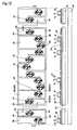
- Fig. 7 shows a top view and a cross-sectional view of the lighting device of the first embodiment with a plurality of the light-emitting devices connected in series.
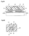
- Fig. 8A shows a cross-sectional view of a light-emitting device of the first embodiment fixed to a metal substrate
- Fig. 8B shows a top view of an optical semiconductor element of the first embodiment having an anode and a cathode on its topside.
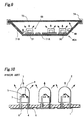
- Fig. 9 shows a cross-sectional view of the lighting device according to a second embodiment of the invention.
- Fig. 10 shows a cross-sectional view of a conventional lighting device.
- Fig. 11A- 11D show cross-sectional views to explain manufacturing steps of the conventional lighting device.
- Fig. 12 shows a top view and a cross-sectional view of a reference lighting device.
- a material for a conductive foil 61 in Fig. 1 is chosen, based on considerations on adhering characteristics to brazing materials, bonding strength and suitability for plating, from a group including copper-based materials, aluminum-based material, Fe (iron) -Ni (nickel), Cu-Al and Al-Cu-Al multilayer film.
- Thickness of the conductive foil is preferably from 10 ⁇ m to 300 ⁇ m in consideration of later process step of etching, and is chosen to be 150 ⁇ m in this embodiment. However, it could be thicker than 300 ⁇ m or thinner than 10 ⁇ m, as long as the separation grooves 64 shallower than the conductive foil 61 could be formed in it as described later.
- the conductive foil 61 could be prepared and supplied in a form of a roll of pre-determined width, or in a form of cut-sheet of a pre-determined size.
- the conductive foil 61 is subject to half-etching with a mask of a photo-resist film 60 having openings on the topside of the conductive foil 61 (backside of the conductive foil is omitted in Fig. 1), and pre-determined regions on the conductive foil 61 are half-etched to form the separation grooves 64.
- the depth of a separation groove 64 formed by the etching is 80 ⁇ m, for example. Since the side of the separation grooves 64 becomes rough surface, adhering strength to a transparent isolation resin 67 is improved.
- the half-etching could be done after a silver film 62, which will be described later, is formed using a mask of a photo-resist film covering the silver film 62.
- a shape of the sidewall of the separation groove varies depending on a removing method.
- the removing method could be either wet etch, dry etch, evaporation by laser, dicing or the like.
- ferric chloride or cupric chloride is mostly adopted as an etchant.
- the conductive foil 61 is dipped into the etchant or showered with the etchant. Since wet etching is isotropic in general, the side of the groove becomes curved.
- the separation grooves can be formed by direct exposure to a laser beam.
- the side of the separation groove 64 is formed rather straight.
- Dicing can form matrix shaped separation grooves, although curved complex pattern is not possible with dicing process.
- a pre-determined area on both sides of the conductive foil 61 is plated.
- a film consist of silver plating hereafter referred to as Ag film 62
- the conductive film is not limited to silver.
- the Ag film 62 can be formed only on the topside of the conductive foil 61.
- the Ag film 62 adheres to both gold and the brazing material. Therefore, with the gold film covering the backside of the die, the die can be bonded to the Ag film 62 on the conductive passage 51 by thermo-compression bonding or through the intermediary of brazing material such as solder. Furthermore, a wire bonding is possible because a gold wire can adhere to the Ag film.
- the Ag film 62 formed on the conductive foil 61 reflects the light emitted from an optical semiconductor element 65, which will be described later. This improves an efficiency of upward light emission.
- the area of Ag film 62 is too wide and reduces contact area between the conductive foil 61 and the isolation resin 67, such a configuration results in falling off, when the conductive foil 61, on which the optical semiconductor element is mounted as described later, is sealed with the isolation resin 67.
- adhering strength of the Ag film 62 to the isolation resin 67 is lower than that of the conductive foil 61 made of copper to the isolation resin 67. Therefore the area to form the Ag film 62 is determined considering both the adhering strength of the conductive foil 61 to the isolation resin 67 and the reflection efficiency of the light from the light-emitting device 68 by the Ag film 62.
- the optical semiconductor element 65 is mounted on and connected to the conductive foil 61 with the separation grooves formed on it as shown in Fig. 3.
- an LED is used as the optical semiconductor element 65.
- the backside of the optical semiconductor element 65 is die-bonded on a first conductive electrode (die pad) 51A, and a metal wire 66 is wire-bonded to connect a topside of the optical semiconductor element 65 and a second conductive electrode 51B.
- a cathode that is the backside of the optical semiconductor element 65 is bonded on the first conductive electrode 51A
- an anode that is the topside of the optical semiconductor element 65 is wire-bonded to the second conductive electrode 51B with the metal wire 66.
- the anode of the optical semiconductor element 65 is bonded on the first conductive electrode 51A
- the cathode of the optical semiconductor element 65 is wire bonded to the second conductive electrode 51B with the metal wire 66.
- the optical semiconductor element 65 is sealed and covered by the isolation resin 67, which is transparent to the light emitted from the optical semiconductor element 65.
- the optical semiconductor element 65 and the conductive foil 61 with the separation groove 64 are sealed with thermosetting silicone resin or epoxy resin, by transfer molding using a mold (not shown in Fig. 4).
- the resin has to be pervious to the light. Therefore a transparent resin or a resin transparent at least to a light of pre-determined wavelength is used.
- each optical semiconductor element 65 is molded individually when it is covered with the transparent resin 67.
- each optical semiconductor element 65 is molded individually when it is covered with the transparent resin 67.
- filler which is used to prevent a warp
- each optical semiconductor element 65 is molded individually when it is covered with the transparent resin 67.
- each optical semiconductor element 65 (each light-emitting device described later) needs to be molded individually.
- the conductive foil works as a supporting substrate until the transparent resin 67 covers the optical semiconductor element.
- Driving capability of the lighting device is improved, since the lighting device of this embodiment has better heat dissipation than conventional one that is constructed as the light-emitting element 2 on the printed circuit board 1 (Refer to Fig. 10).
- the conductive foil 61 that is essential as the electrode material is used also as the supporting substrate, minimizing constituent elements and reducing cost.
- the conductive foil 61 is not separated into conductive passage 51, since the separation grooves 64 are formed to be shallower than the thickness of the conductive foil 61. Therefore it can be processed as a sheet of conductive foil 61, making operation very easy in molding with the transparent resin and carrying and setting it to the mold.
- a process step to remove the backside of the conductive foil 61 chemically and/or physically to separate it into conductive passages 51 is done by polishing, grinding, etching or metal evaporation by a laser.
- the conductive foil 61 is wet etched with a mask of photo-resist film (not shown in Fig. 5) covering entire top surface and portions of the conductive foil 61 to become the conductive passages and the silver film 62 on the backside.
- the conductive foil 61 under the separation grooves 64 is thinned to expose the transparent resin 67 and to separate each conductive passage 51. This forms a structure in which the surface of the conductive passages 51A and 51B (the first and the second electrodes) exposed from the transparent resin 67.
- Another method is to scrape off the backside of the conductive foil 61 by about 50-60 ⁇ m with a polishing apparatus or a grinding apparatus to expose the transparent resin 67 at the separation grooves 64.
- the conductive passage 51 with a thickness of about 40 ⁇ m is separated.
- a flat light-emitting device is realized with the conductive passage 51 embedded in the transparent resin 67 and with the backside of the transparent resin 67 and the backside of the conductive passage 51 coincided with each other.
- the conductive passage 51 When the conductive passage 51 is separated by scraping the backside of the conductive foil 61 with the polishing apparatus or the grinding apparatus, it is possible to apply an anti-oxidation process of the conductive passage 51 by coating the exposed conductive passage 51 with a conductive material such as solder. Coating with an anti-oxidant is also possible.
- the light-emitting device 68 is completed by separating a light-emitting device from adjacent ones with a dicing apparatus as shown in Fig. 6.
- each light-emitting device 68 is separated as copper chips 69 are torn off at both ends of the transparent resin 67 covering the light-emitting device 68 with a press indicated by alternate long and short dashed lines in Fig. 6. Dispensing with deburring process improves workability compared with the dicing or the cutting.
- the manufacturing method of this embodiment is characterized by utilizing the transparent resin 67 as the supporting substrate in the separation process of the conductive passage 51.
- the transparent isolation resin 67 is essential to embed the conductive passage 51. There is no need of a dedicated supporting structure. Therefore, the number of the elements is minimized and the cost is reduced.
- Fig. 7 shows a lighting device 40, in which each of the electrodes 30 is formed on a metal substrate (circuit substrate).
- the light-emitting devices (LEDs) on the electrodes 30 are connected in series to provide a current flowing through the light-emitting devices constant.
- a backside (a first electrode 51A) of a die that makes a cathode (or an anode) of a light-emitting device 68 is attached to a first electrode 30A with a solder 72 (See Fig. 8A).
- a second electrode 51B wire-bonded with an anode (or a cathode) through a metal wire 66 and a second electrode 30B are connected with a solder.
- a backside (a first electrode 51A) of a die that makes a cathode (or an anode) of a next light-emitting device 68 is attached to a second electrode 30B with a solder 72.
- a second electrode 51B wire-bonded with an anode (or a cathode) through a metal wire 66 and a third electrode 30C are connected with a solder 72.
- the series connection is realized by repeating this connection form.
- a melting point (about 140°C) of the solder 72 used in this embodiment is lower than a molding temperature (about 160°C) of the transparent resin. Therefore, the conductive electrodes 51A and 51B, which are metal electrodes of light-emitting device, can be prevented from falling off the mold resin 67 due to a gap or a clack caused by a thermal expansion of the resin 67 when the light-emitting device 68 is soldered to the metal substrate 71.
- An example of low melting point solder is lead (Pb) free tin (Sn) based solder (bismuth (Bi) and antimony (Sb) contained). Solder with a melting point approximately the same as or higher than the molding temperature of the mold resin can be used as well.
- a surface of the copper foil is covered with nickel in order to make it a reflector.
- the light-emitting device 68 is placed at a predetermined location by a robot with an arm movable in the X, Y and Z directions.
- a lighting device with light-emitting devices connected in parallel or a lighting device formed with a combination of parallel connection and serial connection of the light-emitting devices can also realize a lighting device with improved heat dissipation.
- the above-mentioned lighting device 40 is good in workability when it is used as a light source for plant growing, since the light-emitting device 68 can be directly mounted on the metal substrate 71.
- the effectiveness of this invention will be explained in comparison with a reference lighting device shown in Fig. 12, which is not a prior art within the meaning of Art. 54(2) EPC.
- the reference lighting device of a desired size is formed by a complicated process, in which optical semiconductor elements 25 are, first, mounted on a small first metal substrate 23, and then a plurality of the first metal substrates 23 is mounted on a large second metal substrate 24.
- twelve electrodes 30 are formed on the first substrate 23, a backside of a die that makes a cathode (or anode) of an optical semiconductor device 25 (LED) is attached to a first electrode 30A, and an anode (or cathode) and a second electrode 30B are connected with a metal wire 26. A backside of a die of a next optical semiconductor device 25 is attached to the second electrode 30B. An electrode on the surface of the die and a third electrode 30C is connected with a metal wire 26. The series connection is realized by repeating this form of connection. A desired size of the lighting panel is formed by connecting a plurality of the metal substrates 23 by soldering. An isolation resin 27 is potted to cover the optical semiconductor element 25 and the metal wire 26.
- the optical semiconductor elements 25 are mounted on the first metal substrate 23, and then a plurality of the metal substrates 23 is mounted on a second metal substrate 24 to form the reference lighting device of a desired size.
- a need for the process step to mount the optical semiconductor element 25 on the first metal substrate 23 is due to a wire-bonding apparatus used in connecting the anode (or cathode) electrode and each electrode with the metal wire 26.
- the backside of the die which makes a cathode (or anode) of the optical semiconductor element 65 composing the light-emitting device 68 (consisting of the optical semiconductor element 65 (LED) sealed with resin) and the backside of the die wire-bonded to the anode (or cathode) through the metal wire 66 are attached to each electrode 30, as well as the backside of the die that makes the cathode (or anode) of the next optical semiconductor element 65 (LED) and the backside of the die wire-bonded to the anode (or cathode) through the metal wire 66 are attached to each electrode 30, as described before.
- a chip mounting apparatus (a robot with an arm movable in X, Y and Z directions) can handle the substrate of up to 500mm x 500mm.
- the workability is improved by mounting the completed light-emitting devices 68 directly onto the large metal substrate 71 with the chip mounting apparatus.
- the heat dissipation is improved, the supporting substrate is dispensed with, the cost is reduced and the device is smaller, thinner and lighter, since the light-emitting device 68 is directly mounted onto the metal substrate 71.
- each of the completed light-emitting devices 68 is mounted directly onto the metal substrate 71 using the chip mounting apparatus. And thus the workability is improved.
- the optical semiconductor element 25 with the cathode or anode formed on its backside and with the anode or cathode on its topside is used in this embodiment.
- a blue LED is one of the examples of the optical semiconductor element 25A of this structure.
- a metal substrate 71A on which the light-emitting device 68 is mounted has a bent portion 71B in its periphery, which is bent upward to reflect the light from the light-emitting device 68 (optical semiconductor element 25). More light from the optical semiconductor element 25 is emitted upward by the bent portion 71B, which is formed by a pressing process.
- a flat portion is formed at the end of the bent portion 71B.
- a lighting device 40A is completed as a light emitting panel of a desired size, with a transparent panel 73 such as a glass substrate put on the flat portion and fixed to the metal substrate 71A with a fixture 74 such as a rubber packing.
- the lighting device 40A is filled with dry air.
- the transparent panel 73 can be fixed to the metal substrate 71A with a screw.
- a gap between the substrate 71A and the transparent panel 73 is filled with packing such as rubber or sponge. Fixing can be done with an adhesive also.
- this invention makes the constitution of a lighting device possible with minimum components of the optical semiconductor element, conductive passage and the transparent resin without a loss of resources. Therefore no redundant component is required throughout the process, and the light-emitting device can be realized at significantly reduced cost. Also the light-emitting device can be made very small, thin and light by optimizing the thickness of the transparent resin and the thickness of the conductive foil.
- the invention dispenses with the backside electrode and the through hole required in the conventional method, since the backside of the conductive passage is exposed and available for external connection.
- the heat dissipation and the driving capability of the optical semiconductor element are improved compared with the conventional structure, in which the optical semiconductor element is mounted on the printed circuit board.
- the lighting device formed by mounting a plurality of such light-emitting devices directly on the metal substrate can improve heat dissipation, dispense with the supporting substrate to mount light-emitting device and make the lighting device smaller, thinner and lighter.
- the metal substrate has a bent portion in its periphery, which is bent upward to reflect the light from the light-emitting device, more light from the optical semiconductor element is emitted upward by the bent portion.
- the optical semiconductor element can be covered with the transparent panel, minimizing the number of the components to form the lighting device.
- the falling off of the conductive electrode from the mold resin can be prevented by setting the melting point of the solder used in mounting the light-emitting device on the metal substrate lower than the molding temperature of the resin.
- the workability is improved by mounting each of the light-emitting devices directly on the metal substrate using the robot movable horizontally and vertically. Also the workability is improved since only good light-emitting devices are mounted on the metal substrate.
- the conductive foil connecting individual device portions is thinned only after the light-emitting devices are covered with the transparent resin for supporting the light-emitting devices. Then, the individual light-emitting devices are separated from each other. This improves the workability since the conductive foil can be processed as a single sheet until the final processing step where each of the light-emitting devices is separated from each other.
Landscapes
- Led Device Packages (AREA)
- Led Devices (AREA)
Applications Claiming Priority (4)
| Application Number | Priority Date | Filing Date | Title |
|---|---|---|---|
| JP2001224268 | 2001-07-25 | ||
| JP2001224266 | 2001-07-25 | ||
| JP2001224268A JP2003036707A (ja) | 2001-07-25 | 2001-07-25 | 照明装置とその製造方法 |
| JP2001224266A JP2003037296A (ja) | 2001-07-25 | 2001-07-25 | 照明装置とその製造方法 |
Publications (2)
| Publication Number | Publication Date |
|---|---|
| EP1280211A2 true EP1280211A2 (fr) | 2003-01-29 |
| EP1280211A3 EP1280211A3 (fr) | 2006-09-20 |
Family
ID=26619226
Family Applications (1)
| Application Number | Title | Priority Date | Filing Date |
|---|---|---|---|
| EP02016661A Withdrawn EP1280211A3 (fr) | 2001-07-25 | 2002-07-25 | Diode électroluminescente avec dissipation de chaleur améliorée et méthode de fabrication |
Country Status (4)
| Country | Link |
|---|---|
| US (2) | US6696310B2 (fr) |
| EP (1) | EP1280211A3 (fr) |
| CN (2) | CN1222051C (fr) |
| TW (2) | TW591990B (fr) |
Cited By (2)
| Publication number | Priority date | Publication date | Assignee | Title |
|---|---|---|---|---|
| CN105190156A (zh) * | 2013-05-02 | 2015-12-23 | Ccs株式会社 | 照明装置 |
| EP3789655A1 (fr) * | 2012-07-09 | 2021-03-10 | Nichia Corporation | Dispositif électroluminescent |
Families Citing this family (23)
| Publication number | Priority date | Publication date | Assignee | Title |
|---|---|---|---|---|
| JP2004186460A (ja) * | 2002-12-04 | 2004-07-02 | Sanyo Electric Co Ltd | 回路装置の製造方法 |
| EP1627437B1 (fr) * | 2003-05-26 | 2016-03-30 | Panasonic Intellectual Property Management Co., Ltd. | Composant electroluminescent |
| US7256486B2 (en) * | 2003-06-27 | 2007-08-14 | Avago Technologies Ecbu Ip (Singapore) Pte. Ltd. | Packaging device for semiconductor die, semiconductor device incorporating same and method of making same |
| US7919787B2 (en) * | 2003-06-27 | 2011-04-05 | Avago Technologies Ecbu Ip (Singapore) Pte. Ltd. | Semiconductor device with a light emitting semiconductor die |
| US7279355B2 (en) * | 2003-06-27 | 2007-10-09 | Avago Technologies Ecbuip (Singapore) Pte Ltd | Method for fabricating a packaging device for semiconductor die and semiconductor device incorporating same |
| EP1665397A2 (fr) * | 2003-09-16 | 2006-06-07 | Matsushita Electric Industrial Co., Ltd. | Source et appareil d'eclairage par del |
| JP4813484B2 (ja) * | 2004-08-06 | 2011-11-09 | コーニンクレッカ フィリップス エレクトロニクス エヌ ヴィ | 高性能ledランプシステム |
| TW200642109A (en) * | 2005-05-20 | 2006-12-01 | Ind Tech Res Inst | Solid light-emitting display and its manufacturing method |
| KR100784057B1 (ko) | 2005-06-24 | 2007-12-10 | 엘지이노텍 주식회사 | 발광소자 패키지 및 발광소자 패키지 제조 방법 |
| JP2007012682A (ja) * | 2005-06-28 | 2007-01-18 | Shinka Jitsugyo Kk | 光モジュールの製造方法 |
| WO2007111355A1 (fr) * | 2006-03-28 | 2007-10-04 | Kyocera Corporation | Dispositif électroluminescent |
| US7889421B2 (en) | 2006-11-17 | 2011-02-15 | Rensselaer Polytechnic Institute | High-power white LEDs and manufacturing method thereof |
| US8421088B2 (en) * | 2007-02-22 | 2013-04-16 | Sharp Kabushiki Kaisha | Surface mounting type light emitting diode |
| US8604506B2 (en) * | 2007-02-22 | 2013-12-10 | Sharp Kabushiki Kaisha | Surface mounting type light emitting diode and method for manufacturing the same |
| TWI415293B (zh) * | 2007-12-14 | 2013-11-11 | 榮創能源科技股份有限公司 | 光電元件之製造方法及其封裝結構 |
| US7968378B2 (en) * | 2008-02-06 | 2011-06-28 | Infineon Technologies Ag | Electronic device |
| US20110201159A1 (en) * | 2008-11-05 | 2011-08-18 | Mitsui High-Tec, Inc. | Semiconductor package and manufacturing method thereof |
| JP4930548B2 (ja) * | 2009-06-08 | 2012-05-16 | サンケン電気株式会社 | 発光装置及びその製造方法 |
| WO2012092990A2 (fr) | 2011-01-05 | 2012-07-12 | Udo Wenske | Produit médical pour l'amélioration de la fertilité d'un mammifère |
| TWI438375B (zh) * | 2011-11-25 | 2014-05-21 | Lextar Electronics Corp | 光源模組及其光源組件 |
| DE102015106444A1 (de) * | 2015-04-27 | 2016-10-27 | Osram Opto Semiconductors Gmbh | Optoelektronische Bauelementanordnung und Verfahren zur Herstellung einer Vielzahl von optoelektronischen Bauelementanordnungen |
| CN107135603B (zh) * | 2017-06-02 | 2019-10-25 | Oppo广东移动通信有限公司 | 印制电路板及移动终端 |
| WO2020153448A1 (fr) * | 2019-01-24 | 2020-07-30 | 大日本印刷株式会社 | Feuille d'éclairage à del pour la culture d'animaux et de plantes, module d'éclairage à del pour la culture d'animaux et de plantes, plaque d'étagère pour étagère de culture pour animaux et plantes, étagère de culture pour animaux et plantes, usine de culture d'animaux et de plantes, et dispositif d'éclairage à del pour la culture d'animaux et de plantes |
Family Cites Families (19)
| Publication number | Priority date | Publication date | Assignee | Title |
|---|---|---|---|---|
| US534330A (en) * | 1895-02-19 | Electric bell | ||
| US4476620A (en) * | 1979-10-19 | 1984-10-16 | Matsushita Electric Industrial Co., Ltd. | Method of making a gallium nitride light-emitting diode |
| JPS59107584A (ja) * | 1982-12-13 | 1984-06-21 | Casio Comput Co Ltd | 発光ダイオ−ド |
| FR2547087B1 (fr) * | 1983-05-30 | 1985-07-12 | Radiotechnique Compelec | Element de panneau d'affichage a cristaux semi-conducteurs et panneau comportant ledit element |
| JP2511717B2 (ja) * | 1990-02-05 | 1996-07-03 | 三菱電線工業株式会社 | Ledモジュ―ル |
| JP3127195B2 (ja) * | 1994-12-06 | 2001-01-22 | シャープ株式会社 | 発光デバイスおよびその製造方法 |
| JP3992301B2 (ja) * | 1995-04-26 | 2007-10-17 | シチズン電子株式会社 | チップ型発光ダイオード |
| JPH10308536A (ja) * | 1997-05-06 | 1998-11-17 | Mitsubishi Cable Ind Ltd | Ledライン光源 |
| JP4065051B2 (ja) * | 1998-04-17 | 2008-03-19 | スタンレー電気株式会社 | 表面実装ledとその製造方法 |
| JP4215306B2 (ja) * | 1998-08-27 | 2009-01-28 | シチズン電子株式会社 | 半導体のパッケージおよびその製造方法 |
| JP3217322B2 (ja) * | 1999-02-18 | 2001-10-09 | 日亜化学工業株式会社 | チップ部品型発光素子 |
| EP1059668A3 (fr) * | 1999-06-09 | 2007-07-18 | Sanyo Electric Co., Ltd. | Dispositif à circuit intégré hybride |
| FR2794927B1 (fr) * | 1999-06-09 | 2001-08-10 | Ass Pour La Promotion Et Le De | Dispositif d'eclairage polychromatique a diodes electroluminescentes |
| JP3627592B2 (ja) * | 1999-10-08 | 2005-03-09 | 日亜化学工業株式会社 | 発光装置の製造方法 |
| JP2001174671A (ja) * | 1999-12-16 | 2001-06-29 | Japan Aviation Electronics Industry Ltd | 光素子モジュール |
| TW507482B (en) * | 2000-06-09 | 2002-10-21 | Sanyo Electric Co | Light emitting device, its manufacturing process, and lighting device using such a light-emitting device |
| TW506236B (en) * | 2000-06-09 | 2002-10-11 | Sanyo Electric Co | Method for manufacturing an illumination device |
| TW463394B (en) | 2000-12-19 | 2001-11-11 | Taiwan Oasis Technology Co Ltd | Chip-type light emitting diode and its manufacturing method |
| ATE425556T1 (de) * | 2001-04-12 | 2009-03-15 | Matsushita Electric Works Ltd | Lichtquellenbauelement mit led und verfahren zu seiner herstellung |
-
2002
- 2002-07-03 TW TW091114725A patent/TW591990B/zh not_active IP Right Cessation
- 2002-07-09 TW TW091115124A patent/TW595279B/zh not_active IP Right Cessation
- 2002-07-24 US US10/201,610 patent/US6696310B2/en not_active Expired - Fee Related
- 2002-07-24 US US10/198,756 patent/US20030020126A1/en not_active Abandoned
- 2002-07-25 CN CNB02126970XA patent/CN1222051C/zh not_active Expired - Fee Related
- 2002-07-25 EP EP02016661A patent/EP1280211A3/fr not_active Withdrawn
- 2002-07-25 CN CN021269718A patent/CN1217424C/zh not_active Expired - Fee Related
Non-Patent Citations (1)
| Title |
|---|
| None |
Cited By (2)
| Publication number | Priority date | Publication date | Assignee | Title |
|---|---|---|---|---|
| EP3789655A1 (fr) * | 2012-07-09 | 2021-03-10 | Nichia Corporation | Dispositif électroluminescent |
| CN105190156A (zh) * | 2013-05-02 | 2015-12-23 | Ccs株式会社 | 照明装置 |
Also Published As
| Publication number | Publication date |
|---|---|
| CN1399353A (zh) | 2003-02-26 |
| CN1399354A (zh) | 2003-02-26 |
| US20030020126A1 (en) | 2003-01-30 |
| US6696310B2 (en) | 2004-02-24 |
| TW595279B (en) | 2004-06-21 |
| US20030022407A1 (en) | 2003-01-30 |
| CN1217424C (zh) | 2005-08-31 |
| TW591990B (en) | 2004-06-11 |
| CN1222051C (zh) | 2005-10-05 |
| EP1280211A3 (fr) | 2006-09-20 |
Similar Documents
| Publication | Publication Date | Title |
|---|---|---|
| US6696310B2 (en) | Manufacturing method of lighting device | |
| US6558970B2 (en) | Light irradiating device, manufacturing method thereof, and lighting apparatus using the light irradiating device | |
| US6534330B2 (en) | Light irradiating device manufacturing method | |
| EP1680816B1 (fr) | Boitier de puces photoemettrices de puissance a montage en surface | |
| JP4731906B2 (ja) | 電力表面取り付けの発光ダイ・パッケージ | |
| EP1253650B1 (fr) | Diode électroluminescente pour montage en surface et son procédé de fabrication | |
| JP3540769B2 (ja) | 光照射装置とその製造方法及びその光照射装置を用いた照明装置 | |
| US20090197364A1 (en) | Method of fabricating substrate | |
| JP2003036707A (ja) | 照明装置とその製造方法 | |
| KR100610275B1 (ko) | 고출력 발광 다이오드 패키지 및 그 제조방법 | |
| JP2003037297A (ja) | 光照射装置とその製造方法及びその光照射装置を用いた照明装置 | |
| CN113725721A (zh) | 半导体侧发射式激光器的引线框架封装及其制造方法 | |
| JP2003037296A (ja) | 照明装置とその製造方法 | |
| JP2011077048A (ja) | 照明装置 | |
| JP3869633B2 (ja) | 半導体装置の製造方法 | |
| JP2002026180A (ja) | 回路装置の製造方法 |
Legal Events
| Date | Code | Title | Description |
|---|---|---|---|
| PUAI | Public reference made under article 153(3) epc to a published international application that has entered the european phase |
Free format text: ORIGINAL CODE: 0009012 |
|
| AK | Designated contracting states |
Designated state(s): AT BE BG CH CY CZ DE DK EE ES FI FR GB GR IE IT LI LU MC NL PT SE SK TR |
|
| AX | Request for extension of the european patent |
Extension state: AL LT LV MK RO SI |
|
| PUAL | Search report despatched |
Free format text: ORIGINAL CODE: 0009013 |
|
| AK | Designated contracting states |
Kind code of ref document: A3 Designated state(s): AT BE BG CH CY CZ DE DK EE ES FI FR GB GR IE IT LI LU MC NL PT SE SK TR |
|
| AX | Request for extension of the european patent |
Extension state: AL LT LV MK RO SI |
|
| AKX | Designation fees paid | ||
| STAA | Information on the status of an ep patent application or granted ep patent |
Free format text: STATUS: THE APPLICATION IS DEEMED TO BE WITHDRAWN |
|
| 18D | Application deemed to be withdrawn |
Effective date: 20070321 |
|
| REG | Reference to a national code |
Ref country code: DE Ref legal event code: 8566 |