EP1280213A2 - Mehrschichtige leitende Linie aus Silber oder Silberlegierung, Herstellungsverfahren und dieses verwendende Anzeigetafelsubstrat - Google Patents
Mehrschichtige leitende Linie aus Silber oder Silberlegierung, Herstellungsverfahren und dieses verwendende Anzeigetafelsubstrat Download PDFInfo
- Publication number
- EP1280213A2 EP1280213A2 EP02016496A EP02016496A EP1280213A2 EP 1280213 A2 EP1280213 A2 EP 1280213A2 EP 02016496 A EP02016496 A EP 02016496A EP 02016496 A EP02016496 A EP 02016496A EP 1280213 A2 EP1280213 A2 EP 1280213A2
- Authority
- EP
- European Patent Office
- Prior art keywords
- silver
- conductor layer
- silver alloy
- protective conductor
- protective
- Prior art date
- Legal status (The legal status is an assumption and is not a legal conclusion. Google has not performed a legal analysis and makes no representation as to the accuracy of the status listed.)
- Withdrawn
Links
Images



Classifications
-
- H—ELECTRICITY
- H05—ELECTRIC TECHNIQUES NOT OTHERWISE PROVIDED FOR
- H05B—ELECTRIC HEATING; ELECTRIC LIGHT SOURCES NOT OTHERWISE PROVIDED FOR; CIRCUIT ARRANGEMENTS FOR ELECTRIC LIGHT SOURCES, IN GENERAL
- H05B33/00—Electroluminescent light sources
- H05B33/12—Light sources with substantially two-dimensional [2D] radiating surfaces
- H05B33/26—Light sources with substantially two-dimensional [2D] radiating surfaces characterised by the composition or arrangement of the conductive material used as an electrode
-
- H—ELECTRICITY
- H05—ELECTRIC TECHNIQUES NOT OTHERWISE PROVIDED FOR
- H05K—PRINTED CIRCUITS; CASINGS OR CONSTRUCTIONAL DETAILS OF ELECTRIC APPARATUS; MANUFACTURE OF ASSEMBLAGES OF ELECTRICAL COMPONENTS
- H05K3/00—Apparatus or processes for manufacturing printed circuits
- H05K3/02—Apparatus or processes for manufacturing printed circuits in which the conductive material is applied to the surface of the insulating support and is thereafter removed from such areas of the surface which are not intended for current conducting or shielding
- H05K3/06—Apparatus or processes for manufacturing printed circuits in which the conductive material is applied to the surface of the insulating support and is thereafter removed from such areas of the surface which are not intended for current conducting or shielding the conductive material being removed chemically or electrolytically, e.g. by photo-etch process
- H05K3/061—Etching masks
-
- H—ELECTRICITY
- H10—SEMICONDUCTOR DEVICES; ELECTRIC SOLID-STATE DEVICES NOT OTHERWISE PROVIDED FOR
- H10K—ORGANIC ELECTRIC SOLID-STATE DEVICES
- H10K59/00—Integrated devices, or assemblies of multiple devices, comprising at least one organic light-emitting element covered by group H10K50/00
- H10K59/10—OLED displays
- H10K59/17—Passive-matrix OLED displays
- H10K59/179—Interconnections, e.g. wiring lines or terminals
- H10K59/1795—Interconnections, e.g. wiring lines or terminals comprising structures specially adapted for lowering the resistance
-
- H—ELECTRICITY
- H10—SEMICONDUCTOR DEVICES; ELECTRIC SOLID-STATE DEVICES NOT OTHERWISE PROVIDED FOR
- H10K—ORGANIC ELECTRIC SOLID-STATE DEVICES
- H10K59/00—Integrated devices, or assemblies of multiple devices, comprising at least one organic light-emitting element covered by group H10K50/00
- H10K59/80—Constructional details
- H10K59/805—Electrodes
- H10K59/8051—Anodes
- H10K59/80516—Anodes combined with auxiliary electrodes, e.g. ITO layer combined with metal lines
-
- H—ELECTRICITY
- H05—ELECTRIC TECHNIQUES NOT OTHERWISE PROVIDED FOR
- H05K—PRINTED CIRCUITS; CASINGS OR CONSTRUCTIONAL DETAILS OF ELECTRIC APPARATUS; MANUFACTURE OF ASSEMBLAGES OF ELECTRICAL COMPONENTS
- H05K1/00—Printed circuits
- H05K1/02—Details
- H05K1/09—Use of materials for the conductive, e.g. metallic pattern
-
- H—ELECTRICITY
- H05—ELECTRIC TECHNIQUES NOT OTHERWISE PROVIDED FOR
- H05K—PRINTED CIRCUITS; CASINGS OR CONSTRUCTIONAL DETAILS OF ELECTRIC APPARATUS; MANUFACTURE OF ASSEMBLAGES OF ELECTRICAL COMPONENTS
- H05K2201/00—Indexing scheme relating to printed circuits covered by H05K1/00
- H05K2201/03—Conductive materials
- H05K2201/0332—Structure of the conductor
- H05K2201/0335—Layered conductors or foils
- H05K2201/0338—Layered conductor, e.g. layered metal substrate, layered finish layer or layered thin film adhesion layer
-
- H—ELECTRICITY
- H05—ELECTRIC TECHNIQUES NOT OTHERWISE PROVIDED FOR
- H05K—PRINTED CIRCUITS; CASINGS OR CONSTRUCTIONAL DETAILS OF ELECTRIC APPARATUS; MANUFACTURE OF ASSEMBLAGES OF ELECTRICAL COMPONENTS
- H05K2203/00—Indexing scheme relating to apparatus or processes for manufacturing printed circuits covered by H05K3/00
- H05K2203/05—Patterning and lithography; Masks; Details of resist
- H05K2203/0562—Details of resist
- H05K2203/0577—Double layer of resist having the same pattern
-
- H—ELECTRICITY
- H05—ELECTRIC TECHNIQUES NOT OTHERWISE PROVIDED FOR
- H05K—PRINTED CIRCUITS; CASINGS OR CONSTRUCTIONAL DETAILS OF ELECTRIC APPARATUS; MANUFACTURE OF ASSEMBLAGES OF ELECTRICAL COMPONENTS
- H05K2203/00—Indexing scheme relating to apparatus or processes for manufacturing printed circuits covered by H05K3/00
- H05K2203/11—Treatments characterised by their effect, e.g. heating, cooling, roughening
- H05K2203/1184—Underetching, e.g. etching of substrate under conductors or etching of conductor under dielectrics; Means for allowing or controlling underetching
-
- H—ELECTRICITY
- H05—ELECTRIC TECHNIQUES NOT OTHERWISE PROVIDED FOR
- H05K—PRINTED CIRCUITS; CASINGS OR CONSTRUCTIONAL DETAILS OF ELECTRIC APPARATUS; MANUFACTURE OF ASSEMBLAGES OF ELECTRICAL COMPONENTS
- H05K3/00—Apparatus or processes for manufacturing printed circuits
- H05K3/02—Apparatus or processes for manufacturing printed circuits in which the conductive material is applied to the surface of the insulating support and is thereafter removed from such areas of the surface which are not intended for current conducting or shielding
- H05K3/06—Apparatus or processes for manufacturing printed circuits in which the conductive material is applied to the surface of the insulating support and is thereafter removed from such areas of the surface which are not intended for current conducting or shielding the conductive material being removed chemically or electrolytically, e.g. by photo-etch process
- H05K3/061—Etching masks
- H05K3/062—Etching masks consisting of metals or alloys or metallic inorganic compounds
Definitions
- the present invention relates to a conductive wiring comprising silver or silver alloy and to a display panel substrate using the same.
- a display panel substrate there is an organic electroluminescence display panel for example.
- the organic electroluminescence display panel has a plurality of organic electroluminescence devices formed on the substrate in a predetermined pattern.
- Each organic electroluminescence device comprises one or more thin films of organic compound materials at least one of which exhibits the electroluminescence (hereinafter also referred to as "EL") which is emits light in response to a current injected thereinto.
- EL electroluminescence
- the organic EL device includes a transparent electrode as an anode, at least one organic compound thin film and a metal electrode as a cathode, which are laminated on a transparent substrate in due order.
- the organic compound thin film (so-called “organic functional layer” ) may be a single light emitting layer, or a laminate which includes a three-layer structure composed of an organic hole transport layer, a light emitting layer and an organic electron transport layer, or a two-layer structure composed of an organic hole transport layer and a light emitting layer.
- the organic EL device may also include an electron or hole injection layer inserted between appropriate ones of these layers.
- such a matrix type EL display panel has an image display array comprised of a plurality of light emitting pixels of organic EL devices arranged at respective intersections of intersecting rows and columns.
- the matrix display type one is composed of row electrodes including transparent electrode layers, organic functional layers, and column electrodes including metal electrode layers which intersect the row electrodes. These layers are laminated in sequence.
- the row electrodes are each formed in a strip shape, and arranged in parallel with each other with a predetermined spacing therebetween. The same is applied as well to the column electrodes.
- the display panel of matrix type has a display array region comprised of light emitting pixels which are formed of a plurality of organic EL devices positioned at respective intersections of a plurality of row electrodes with a plurality of column electrodes.
- the organic EL device Since the organic EL device is of an electric current injection type, its consumption of electric power greatly depends on the resistivity of the electrode line. Thus, a low resistive material is strongly required for the row and column electrodes of the organic EL device otherwise a serious voltage drop occurs as involving in the luminance inhomogeneousness to ruin the display quality.
- the transparent electrode materials used for the anode such as indium tin oxide (ITO) or the like have high sheet resistance values, although a low resistive material is required for the wiring line connecting the electrodes to each other in the display array region of the substrate.
- ITO indium tin oxide
- the conventional manufacturing process of the EL display panel involves the steps of patterning the ITO anodes on the substrate, patterning the auxiliary metal lines, patterning the organic functional layers, patterning the ramparts, patterning the cathodes and connecting the cathodes and anodes to the corresponding external terminals.
- an indispensable condition of the electrode material is to have a low resistivity.
- Aluminum (Al) based materials is generally known as a low resistivity wiring material.
- the resistivity of the thin-film is limited at approximately 4 ⁇ cm at most.
- the Al-based materials for the wiring lines on the organic EL display panel it is a problem that the Al-based materials shows an electrochemical reaction with ITO generally used for the transparent electrode.
- the present invention has been made in view of the problem mentioned above, and an object thereof is to provide wiring lines of a silver (Ag) or silver alloy wiring enabling to lower the electric resistance of the wiring on a substrate, and to improve the oxidation proof of the Ag-based wiring material. Another object of the present invention is to provide a display panel substrate with the wiring lines of silver or silver alloy bringing about a high display quality.
- a layered wiring line of silver or silver alloy comprising: a silver or silver alloy conductor layer including silver or silver alloy; and a protective conductor layer layered on and covering the silver or silver alloy conductor layer.
- a thickness of said protective conductor layer is set in such a manner that, in a case that said silver or silver alloy conductor layer and the protective conductor layer keep in contact with a liquid etchant, a ratio of (said protective conductor layer's thickness) / (said silver or silver alloy conductor layer's thickness) is less than that of (a solution velocity of said protective conductor layer in said liquid etchant) / (a solution velocity of said silver or silver alloy conductor layer in said liquid etchant).
- a method for forming a layered wiring line of silver or silver alloy including a silver or silver alloy conductor layer including silver or silver alloy and a protective conductor layer layered on and covering the silver or silver alloy conductor layer, the method comprising the steps of:
- a display panel substrate having a display array region comprising:
- the display panel substrate according to the present invention further comprises organic electroluminescence devices each having organic functional layers and placed at the display electrodes.
- the general substrate treatment includes a UV/O 3 cleaning (Japanese patent Application Kokai No. 2001-311869) and an O 2 plasma treatment (C. C. Wu, C. I. Wu, J. C. Sturm, and A. Kahn, Appl. Phys. Lett. vol. 70 No. 11 1348 (1997)).
- the substrate is generally subjected to the UV/O 3 cleaning or O 2 plasma treatment, before the formation of the organic functional layers, to improve the luminescence efficiency of the device.
- the wiring is preformed using the Ag-based material in a single layer form for auxiliary electrodes to be connected to the transparent electrodes on the substrate. Then the UV/O 3 cleaning or O 2 plasma treatment is conducted on the substrate and the organic functional layers are formed on the electrodes. Since the auxiliary electrodes of Ag-based material are oxidized to increase the resistivity of the whole wiring lines, there is a difficult limit to the acquisition of a high performance organic EL display panel.
- Inventors propose a multi layered wiring using Ag-based materials in the multi layer form instead of the single layer form i.e., which comprises: a silver or silver alloy conductor layer including silver or silver alloy; and a protective conductor layer layered on and covering said silver or silver alloy conductor layer.
- the protective conductor layer meets the following requirements (1) - (9) of characteristics and conditions:
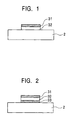
- a silver or silver alloy conductor layer 32 and a protective conductor layer 31 are layered in turn on a substrate 2 so as to be a multi layered wiring line.
- the protective conductor layer 31 covers and protects the underlaid silver or silver alloy conductor layer 32 to prevent oxidation of the conductor layer 32.
- the multi layered wiring line keeps its low resistance and increases the oxidation proof thereof so as to enhance the durability against the substrate treatment such as UV/O 3 cleaning and O 2 plasma treatment as well as the environmental resistance thereof.
- the protective conductor layer 31 is formed by a material having an oxidation proof higher than that of the silver or silver alloy conductor layer 32 and alternatively by a material failing to exhibit a marked rise of resistivity thereof even when being oxidized.
- the protective conductor layer 31 have a durable thickness against the predetermined substrate treatment or having an environmental resistance within a thin thickness range as possible. Concretely it is preferable that the protective conductor layer 31 has a thickness of 50-1000 ⁇ as dependent on the martial thereof. Of course a high adherence between both the layers is preferable.
- a second protective conductor layer 33 may be provided between the underlaid silver or silver alloy conductor layer 32 and the substrate 2 to prevent an invasion of oxygen from the substrate 2 to the silver or silver alloy conductor layer 32.
- the silver or silver alloy conductor layer 32 and the protective conductor layers 31 and 33 are formed by sputtering, evaporation, CVD (chemical vapor deposition) or the like.
- the silver or silver alloy conductor layer 32 may be composed of Ag simplex or Ag alloy consisting of Ag and optional other substances.
- the Ag alloy may contain any substances of any kinds.
- the amount of the added substances other than Ag is less than 10 wt.% preferably, i.e., Ag amount is equal to or more than 90 wt.%, because the resistivity of the wiring is proportional to the amount of the substances other than Ag.
- Table 1 shows electrical characteristics of various Ag alloy films.
- the material of the protective conductor layer 31 is selected from materials each having oxidation proof higher than that of the underlaid silver or silver alloy conductor layer 32, or materials each failing to exhibit a marked rise of resistivity thereof when being oxidized.
- the high oxidation proof materials are preferably materials having high melt points such as Cr, Ta, W, Ti, Mo or the like or a simplex thereof or alloy including the same.
- metal oxide such as Al simplex or Al alloy, ITO, indium zinc oxide (IZO), tin oxide, zinc oxide, indium oxide, magnesium oxide or the like, metal fluoride, metal nitride or the like.
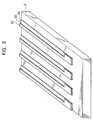
- FIG. 3 shows a layered wiring line of silver or silver alloy on the organic EL display panel substrate according to another embodiment of the present invention.
- the layered wiring line of silver or silver alloy is used for an auxiliary electrode connected to a stripe transparent electrode 3a i.e., anode of ITO in the organic EL device.
- the underlaid silver or silver alloy conductor layer 32 is contact with the ITO anode previously formed on the substrate 2.
- the layered wiring line of silver or silver alloy should have both a high conductivity sufficient to prevent the rise of resistance in the thickness direction and a low contact resistance to metal or the like.
- Ag-0.9Pd-1Cu alloy (hereinafter also referred to as "APC" wherein numerals denote ratios wt.% of added inclusion) is deposited by sputtering at a 2000 ⁇ thickness on a glass substrate of 30 mm ⁇ 30 mm as a silver or silver alloy conductor layer.
- APC Ag-0.9Pd-1Cu alloy
- APC Ag-0.9Pd-1Cu alloy
- the latticework is formed on the lamination of the silver or silver alloy conductor layer and the protective conductor layer on each sample in such a manner that eleven deep cuts are made in rows and columns at a 1 mm interval respectively so as to arrange 100 pieces of squares as a check pattern. Then an adhesive tape is put on each sample having the check pattern. After that, the adhesive tape is peeled at a predetermined velocity from the check pattern to separate the squares of lamination from the substrate of each sample. By count of remaining squares on the substrate, the adherence of lamination is evaluated on each sample. Since it marks on a maximum scale of 100 points, 100/100 is the perfect score and 0/100 is the minimum score. Table 2 shows those results in the column of Adherence. There is no peeling between the silver or silver alloy conductor layer and the protective conductor layer every sample.
- the low resistivity wiring material is processed to a minute pattern.
- the minute patterning utilizes generally the photolithography.
- the photolithography patterning of the wiring material requires two etching steps both for the protective conductor layer and the silver or silver alloy conductor layer and thus the manufacture of device may involve many more steps than that of a single layer of the silver or silver alloy conductor layer.
- the protective conductor layer material is selected from a group substances capable of being etched by the same conditions as the silver or silver alloy conductor layer in order to use a liquid etchant in common to the silver or silver alloy conductor layer and the protective conductor layer by a predetermined pattern.
- the protective conductor layer material should have a sufficient durability against the treatment liquid used in the photolithography step such as a developing solution for the photoresist, a peeling solution or the like.
- the silver or silver alloy conductor layer generally has a large etching rate, particularly a fast progress of side-etching in the wet etching. Therefore, in the wet etching, the concurrent etching process is preformed as shown in FIGs. 4-6.
- FIG. 4 shows the end of etching a thick protective conductor layer 31 which is layered on the silver or silver alloy conductor layer 32. From the top of FIG. 4, the etching proceeds downward in the arrow direction to the bottom of the protective conductor layer and then the underlaid silver or silver alloy conductor layer 32 is exposed.
- FIG. 5 shows the state of the etching at the middle of the silver or silver alloy conductor layer 32. Since the silver or silver alloy conductor layer 32 has the fast side-etching progress, it is side-etched faster than the thick protective conductor layer 31. The bottom edge of the thick protective conductor layer 31 is dissolved from the bottom by the etchant entering the side-etched portion of the underlaid silver or silver alloy conductor layer 32 as shown in the right angled arrow direction of FIG. 5.
- FIG. 6 shows the completion of the concurrent etching. Since the side-etched amount of the thick protective conductor layer 31 is small in comparison with that of the silver or silver alloy conductor layer 32, the multi layered wiring line has a section profile formed in an overhanging "T-shape".
- the overlaid protective conductor layer is easily peeled from the underlaid silver or silver alloy conductor layer. As a result, such peeling causes defective products.
- the protective conductor layer material having a side-etched property more than that of the underlaid silver or silver alloy conductor layer.
- Ag-based layer generally has a very high side-etched property. There is few materials having a side-etched property larger than that of Ag-based layer.
- the thickness of the protective conductor layer material should be set in such a manner that a ratio of (the protective conductor layer's thickness) / (the silver or silver alloy conductor layer's thickness) is less than that of (the protective conductor layer's etching rate) / (the silver or silver alloy conductor layer's etching rate).
- the concurrent etching process proceeds as shown in FIGs. 7-9 to obtain a good sectional form of wiring pattern, even if a material for the protective conductor layer has a low side-etched property.
- FIG. 7 shows the end of etching a thin protective conductor layer 31 which is layered on the silver or silver alloy conductor layer 32. From the top of FIG. 7, the etching proceeds downward in the arrow direction to the bottom of the protective conductor layer and then the underlaid silver or silver alloy conductor layer 32 is exposed.
- FIG. 8 shows the state of the etching at the middle of the silver or silver alloy conductor layer 32.
- the silver or silver alloy conductor layer 32 is side-etched faster than the thin protective conductor layer 31 since it has the fast side-etching progress.
- the thin protective conductor layer 31 is rapidly dissolved from the bottom thereof by the etchant entering the side-etched portion of the silver or silver alloy conductor layer 32 because the protective conductor layer 3 has a specific thickness provided above.
- FIG. 9 shows the completion of the concurrent etching. Since the protective conductor layer 31 is thin, it is dissolved at the substantially same level of the silver or silver alloy conductor layer 32 by the etchant entering the side-etched portion thereof. As a result, no portion thought to be overhung like FIG. 6 is perfectly dissolved, so that the resultant multi layered wiring line has a good section profile such as a rectangle form as shown in FIG. 1.
- the protective conductor layer has an etching rate of 5 ⁇ /sec. and the silver or silver alloy conductor layer has an etching rate of 50 ⁇ /sec.
- the ratio of (the protective conductor layer's etching rate) / (the silver or silver alloy conductor layer's etching rate) is 1/10.
- the protective conductor layer should have the minimum thickness sufficient for durability against the predetermined substrate treatment.
- Ag-0.9Pd-1Cu alloy is used for the silver or silver alloy conductor layer and IZO is used for the protective conductor layer. Both the layers are etched by the liquid etchant of aqueous mixture consisting of phosphoric acid, nitric acid and acetic acid respectively, and then the etching rates thereof are measured. As a result, APC has approximately 32 ⁇ /sec. and IZO has approximately 4 ⁇ /sec. in the stable dissolution state at a ratio 1/8 of the etching rates IZO/APC.
- APC is deposited by sputtering at a 2000 ⁇ thickness on a glass substrate of 30 mm ⁇ 30 mm as the silver or silver alloy conductor layer.
- a plurality of such substrates with APC layer are prepared.
- IZO is deposited by sputtering on the APC layer as the protective conductor layer at a thickness of 100 ⁇ as well as at 200 ⁇ , at 300 ⁇ and at 500 ⁇ for each substrate.
- Each sample is etched by the liquid etchant of aqueous mixture consisting of phosphoric acid, nitric acid and acetic acid. After that, the remaining resist is peeled and then the resultant pattern is observed. Table 3 shows those results.
- the protective conductor layer is layered on the Ag-based material layer under a necessary and sufficient condition for the thickness thereof. Therefore it is possible to use the Ag-based material on the printed circuit substrate while retaining its low resistivity in the high oxidation proof and high environmental resistance, although such a retainment is difficult conventionally.
- the multi layered wiring line according to the present invention is pertinent to the organic EL device application, because UV/O 3 cleaning or O 2 plasma treatment can be preformed before the formation of the organic functional layers to obtain an organic EL device having a high luminescence efficiency, although such treatments are conventionally difficult before the formation of the organic functional layers.
- the protective conductor layer and the underlaid silver or silver alloy conductor layer can be dissolved and removed under the same etching conditions, so that the multi layered wiring line can be patterned similarly to the single layer made of the Ag-based material.
- the thickness of the protective conductor layer material is set in such a manner that a ratio of (the protective conductor layer's thickness) /(the silver or silver alloy conductor layer's thickness) is less than that of (the protective conductor layer's etching rate) /(the silver or silver alloy conductor layer's etching rate), so that the multi layered wiring line can obtain a good wiring pattern having a pertinent sectional form.
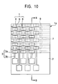
- FIG. 10 is a partially enlarged front view of an organic EL display panel according to another embodiment, viewed through the panel from the front.
- the organic EL display panel has an image display array region 1a comprised of a plurality of light emitting pixels 1 which are arranged in matrix on a transparent substrate 2 made of glass or the like.
- Each of light emitting pixels consists of light emitting portions for red R, green G and blue B emissions .
- a light emitting portion, i.e., organic EL device is formed at the position of an insular transparent electrode 3a at an intersection of a first display electrode line 3 in the horizontal direction, i.e., an anode, and a second display electrode line 9 in the vertical direction, i.e., a cathode.
- the first display electrode 3, i.e., the anode comprises an auxiliary electrode 3b which electrically connects the insular transparent electrodes 3a in the horizontal direction.
- the organic EL display panel comprises a plurality of ramparts 7 disposed between the organic EL devices on the substrate 2.
- the layered wiring line of silver or silver alloy according to the present invention is adapted to the auxiliary electrode 3b connected to the anode of the first display electrode 3 as well as the cathode of the second display electrode line 9.
- the auxiliary electrode 3b consists of the silver or silver alloy conductor layer 32 and the protective conductor layer 31 which are layered in turn on the substrate 2.
- the cathode of the second display electrode line 9 consists of the silver or silver alloy conductor layer 92 and the protective conductor layer 91 which are layered in turn on the organic functional layers 8 after the formation of the rampart 7.
- the ramparts 7 and the organic EL devices are covered with protective coatings 50.
- Each of the organic EL devices is comprised of a first display electrode line 3, one or more organic functional layers 8 including a light emitting layer made of an organic compound, and a second display electrode 9, laminated in order on a substrate 2.
- the ramparts 7 are disposed between the organic EL devices such that they protrude from the substrate.
- each of the organic EL devices is fabricated by vapor depositing or sputtering an anode 3 as an optically transparent first display electrode made of ITO on the transparent glass substrate 2.
- a hole injection layer made of copper phtahlocyanine; a hole transport layer made of TPD (triphenylamine derivative); a light emitting layer made of Alq3 (aluminum chelate complex); and an electron injection layer made of Li2O (lithium oxide) are sequentially vapor deposited to form the organic functional layer 8.
- a cathode 9 made of aluminum (Al) is deposited by vapor deposition to oppose the electrode pattern of the anode 3 as a second display electrode.
- the first display electrode line 3 may be covered with an insulating film 6 except for a pixel portion of the insular transparent electrode 3a.
- the protective coatings 50 comprises an internal inorganic passivation film which covers organic EL devices and the ramparts 7; a sealing film made of a resin for covering the internal inorganic passivation film; and an inorganic passivation film made of an inorganic material for covering the sealing film.
- the internal inorganic passivation film is made of a nitride such as silicon nitride, an oxide, or an inorganic material such as carbon.
- a resin comprising the sealing film a fluorine-based or silicon-based resin, or a synthetic resin such as a photo resist, polyimide and so on may be used.
- the multi layered wiring enables to lower the resistance of wiring or connecting lines of the printed circuit.
- the display panel substrate of the present invention can realize a high quality display panel without luminance inhomogeneousness.
Landscapes
- Engineering & Computer Science (AREA)
- Manufacturing & Machinery (AREA)
- Microelectronics & Electronic Packaging (AREA)
- Electroluminescent Light Sources (AREA)
- Devices For Indicating Variable Information By Combining Individual Elements (AREA)
- Transforming Electric Information Into Light Information (AREA)
- Internal Circuitry In Semiconductor Integrated Circuit Devices (AREA)
- Manufacturing Of Electric Cables (AREA)
Applications Claiming Priority (2)
| Application Number | Priority Date | Filing Date | Title |
|---|---|---|---|
| JP2001222024A JP4620298B2 (ja) | 2001-07-23 | 2001-07-23 | 銀若しくは銀合金配線及びその形成方法並びに表示パネル基板 |
| JP2001222024 | 2001-07-23 |
Publications (2)
| Publication Number | Publication Date |
|---|---|
| EP1280213A2 true EP1280213A2 (de) | 2003-01-29 |
| EP1280213A3 EP1280213A3 (de) | 2006-10-11 |
Family
ID=19055584
Family Applications (1)
| Application Number | Title | Priority Date | Filing Date |
|---|---|---|---|
| EP02016496A Withdrawn EP1280213A3 (de) | 2001-07-23 | 2002-07-23 | Mehrschichtige leitende Linie aus Silber oder Silberlegierung, Herstellungsverfahren und dieses verwendende Anzeigetafelsubstrat |
Country Status (6)
| Country | Link |
|---|---|
| US (1) | US7235883B2 (de) |
| EP (1) | EP1280213A3 (de) |
| JP (1) | JP4620298B2 (de) |
| KR (1) | KR100561232B1 (de) |
| CN (1) | CN1312965C (de) |
| TW (1) | TW550989B (de) |
Cited By (4)
| Publication number | Priority date | Publication date | Assignee | Title |
|---|---|---|---|---|
| WO2005022634A3 (en) * | 2003-08-25 | 2005-04-14 | Eastman Kodak Co | Tapered drain-anode connectors in active matrix oled |
| CN100452112C (zh) * | 2003-09-30 | 2009-01-14 | 旭硝子株式会社 | 带配线的基体形成用层积体、带配线的基体及它们的制造方法 |
| EP1850390A3 (de) * | 2006-04-28 | 2011-11-30 | LG Display Co., Ltd. | Anzeigevorrichtungsmodul |
| CN115064300A (zh) * | 2022-08-18 | 2022-09-16 | 西安拓库米电子科技有限公司 | 一种片式电阻免镀镍用银导体浆料 |
Families Citing this family (25)
| Publication number | Priority date | Publication date | Assignee | Title |
|---|---|---|---|---|
| KR100504472B1 (ko) * | 2002-09-05 | 2005-08-04 | 엘지전자 주식회사 | 유기 el 소자 및 그 제조 방법 |
| JP2005011793A (ja) * | 2003-05-29 | 2005-01-13 | Sony Corp | 積層構造の製造方法および積層構造、表示素子ならびに表示装置 |
| JP2009004383A (ja) * | 2003-05-29 | 2009-01-08 | Sony Corp | 表示装置の製造方法 |
| TWI238449B (en) | 2003-06-06 | 2005-08-21 | Pioneer Corp | Organic semiconductor device and method of manufacture of same |
| JP4405767B2 (ja) * | 2003-08-28 | 2010-01-27 | ソニー株式会社 | 銀及び/又は銀合金を含む基板のフォトレジスト剥離液組成物、それを用いたパターンの製造方法ならびにそれを含む表示装置 |
| JP4225238B2 (ja) * | 2004-04-21 | 2009-02-18 | セイコーエプソン株式会社 | 有機el装置の製造方法及び有機el装置並びに電子機器 |
| KR100801331B1 (ko) * | 2004-09-10 | 2008-02-05 | (주)케이디티 | 유기 전계 발광 소자 및 그 제작 방법 |
| KR100700015B1 (ko) | 2004-11-26 | 2007-03-26 | 삼성에스디아이 주식회사 | 평판표시장치 및 그 제조방법 |
| KR101282397B1 (ko) | 2004-12-07 | 2013-07-04 | 삼성디스플레이 주식회사 | 표시 장치용 배선, 상기 배선을 포함하는 박막 트랜지스터표시판 및 그 제조 방법 |
| TWI332720B (en) | 2005-07-29 | 2010-11-01 | Kyocera Corp | Organic electrolum9iniscence element and its fabrication method |
| KR20070019458A (ko) * | 2005-08-12 | 2007-02-15 | 삼성전자주식회사 | 배선 및 그 형성 방법과 박막 트랜지스터 기판 및 그 제조방법 |
| US20090039775A1 (en) * | 2005-09-12 | 2009-02-12 | Idemitsu Kosan Co., Ltd. | Conductive laminate and organic el device |
| JP4971618B2 (ja) * | 2005-09-30 | 2012-07-11 | ジオマテック株式会社 | 表示用電極パターン製造方法 |
| JP4944596B2 (ja) * | 2006-12-25 | 2012-06-06 | エルジー ディスプレイ カンパニー リミテッド | 有機elディスプレイの製造方法 |
| US7722422B2 (en) * | 2007-05-21 | 2010-05-25 | Global Oled Technology Llc | Device and method for improved power distribution for a transparent electrode |
| JP2009187774A (ja) * | 2008-02-06 | 2009-08-20 | Rohm Co Ltd | 有機エレクトロルミネセンス素子 |
| JP4743645B2 (ja) * | 2008-03-28 | 2011-08-10 | 日立金属株式会社 | 金属薄膜配線 |
| JP5638599B2 (ja) | 2010-03-05 | 2014-12-10 | パイオニア株式会社 | 有機elパネル及びその製造方法 |
| JP5559640B2 (ja) * | 2010-08-25 | 2014-07-23 | 独立行政法人産業技術総合研究所 | 構造体の製造方法 |
| JP2012054006A (ja) * | 2010-08-31 | 2012-03-15 | Gunze Ltd | 透明導電性ガスバリヤフィルム及びその製造方法 |
| US9119272B2 (en) | 2010-12-24 | 2015-08-25 | Nec Lighting, Ltd. | Organic electroluminescent element and organic electroluminescent lighting device |
| CN103151100B (zh) * | 2013-02-06 | 2014-08-06 | 南昌欧菲光科技有限公司 | 导电膜、导电膜制造方法及其触摸屏 |
| JP5976970B1 (ja) | 2015-02-24 | 2016-08-24 | 日東電工株式会社 | 光透過性フィルム |
| CN107342220B (zh) * | 2017-06-26 | 2019-07-02 | 云谷(固安)科技有限公司 | 金属材料图形化方法 |
| KR102734417B1 (ko) * | 2019-01-31 | 2024-11-26 | 삼성디스플레이 주식회사 | 표시 장치 |
Family Cites Families (25)
| Publication number | Priority date | Publication date | Assignee | Title |
|---|---|---|---|---|
| DE68923061T2 (de) * | 1988-11-16 | 1995-11-09 | Mitsubishi Electric Corp | Sonnenzelle. |
| JPH02253593A (ja) | 1989-03-27 | 1990-10-12 | Mitsui Toatsu Chem Inc | 発光素子 |
| JPH05102154A (ja) * | 1991-10-07 | 1993-04-23 | Sony Corp | 半導体装置 |
| KR100211710B1 (ko) * | 1993-10-28 | 1999-08-02 | 미따라이 하지메 | 전자원 및 이를 사용하는 화상 형성 장치와 전자원의 제조 및 구동 방법 |
| EP0736892B1 (de) * | 1995-04-03 | 2003-09-10 | Canon Kabushiki Kaisha | Verfahren zur Herstellung einer elektronenemittierende Vorrichtung, einer Elektronenquelle und eines Bilderzeugungsgerätes |
| JPH0926602A (ja) * | 1995-07-12 | 1997-01-28 | Sony Corp | アクティブマトリクス表示装置 |
| TW364275B (en) | 1996-03-12 | 1999-07-11 | Idemitsu Kosan Co | Organic electroluminescent element and organic electroluminescent display device |
| JPH09260064A (ja) * | 1996-03-15 | 1997-10-03 | Sony Corp | 光学的素子及びその製造方法 |
| JPH1131590A (ja) * | 1997-07-09 | 1999-02-02 | Tdk Corp | 有機el素子 |
| JPH1187052A (ja) * | 1997-09-09 | 1999-03-30 | Futaba Corp | 有機エレクトロルミネッセンス素子 |
| US6303218B1 (en) * | 1998-03-20 | 2001-10-16 | Kabushiki Kaisha Toshiba | Multi-layered thin-film functional device and magnetoresistance effect element |
| KR100267964B1 (ko) * | 1998-07-20 | 2000-10-16 | 구자홍 | 유기 이엘(el) 디스플레이 패널 및 그 제조 방법 |
| JP4608105B2 (ja) | 1999-04-02 | 2011-01-05 | 出光興産株式会社 | 有機エレクトロルミネッセンス表示装置およびその製造方法 |
| JP4465740B2 (ja) | 1999-06-21 | 2010-05-19 | 凸版印刷株式会社 | 電極基板の製造方法 |
| US6157257A (en) * | 1999-06-30 | 2000-12-05 | Conexant Systems, Inc. | Low power folding amplifier |
| EP1076368A2 (de) * | 1999-08-11 | 2001-02-14 | Eastman Kodak Company | Oberflächenemitierende organische elektrolumineszente Diode |
| JP2001102325A (ja) * | 1999-09-30 | 2001-04-13 | Toyoshima Seisakusho:Kk | Ag合金薄膜及びその成膜用スパッタリングターゲット |
| US6492275B2 (en) * | 2000-01-21 | 2002-12-10 | Advanced Micro Devices, Inc. | Control of transistor performance through adjustment of spacer oxide profile with a wet etch |
| JP2001223365A (ja) * | 2000-02-10 | 2001-08-17 | Fujitsu Ltd | 薄膜トランジスタ及びその製造方法 |
| JP3617458B2 (ja) * | 2000-02-18 | 2005-02-02 | セイコーエプソン株式会社 | 表示装置用基板、液晶装置及び電子機器 |
| JP2001242483A (ja) * | 2000-02-25 | 2001-09-07 | Hitachi Ltd | 液晶表示装置及びその配線構造 |
| JP2001351778A (ja) | 2000-06-08 | 2001-12-21 | Tohoku Pioneer Corp | 有機エレクトロルミネッセンス表示デバイス及びその製造方法 |
| JP4592875B2 (ja) * | 2000-06-12 | 2010-12-08 | Nec液晶テクノロジー株式会社 | フレキシブル配線基板及びその製造方法並びに表示装置 |
| US6459464B1 (en) * | 2000-08-14 | 2002-10-01 | Kabushiki Kaisha Advanced Display | Liquid crystal display device with reduced weighting trace defects |
| CN2482313Y (zh) | 2001-06-08 | 2002-03-13 | 谢世辉 | 一种软式印刷电路板结构 |
-
2001
- 2001-07-23 JP JP2001222024A patent/JP4620298B2/ja not_active Expired - Fee Related
-
2002
- 2002-07-19 TW TW091116136A patent/TW550989B/zh active
- 2002-07-19 US US10/197,877 patent/US7235883B2/en not_active Expired - Fee Related
- 2002-07-22 KR KR1020020042836A patent/KR100561232B1/ko not_active Expired - Fee Related
- 2002-07-23 EP EP02016496A patent/EP1280213A3/de not_active Withdrawn
- 2002-07-23 CN CNB021429898A patent/CN1312965C/zh not_active Expired - Fee Related
Cited By (4)
| Publication number | Priority date | Publication date | Assignee | Title |
|---|---|---|---|---|
| WO2005022634A3 (en) * | 2003-08-25 | 2005-04-14 | Eastman Kodak Co | Tapered drain-anode connectors in active matrix oled |
| CN100452112C (zh) * | 2003-09-30 | 2009-01-14 | 旭硝子株式会社 | 带配线的基体形成用层积体、带配线的基体及它们的制造方法 |
| EP1850390A3 (de) * | 2006-04-28 | 2011-11-30 | LG Display Co., Ltd. | Anzeigevorrichtungsmodul |
| CN115064300A (zh) * | 2022-08-18 | 2022-09-16 | 西安拓库米电子科技有限公司 | 一种片式电阻免镀镍用银导体浆料 |
Also Published As
| Publication number | Publication date |
|---|---|
| US20030085403A1 (en) | 2003-05-08 |
| CN1402604A (zh) | 2003-03-12 |
| US7235883B2 (en) | 2007-06-26 |
| CN1312965C (zh) | 2007-04-25 |
| EP1280213A3 (de) | 2006-10-11 |
| JP2003036037A (ja) | 2003-02-07 |
| JP4620298B2 (ja) | 2011-01-26 |
| TW550989B (en) | 2003-09-01 |
| KR100561232B1 (ko) | 2006-03-15 |
| KR20030011566A (ko) | 2003-02-11 |
Similar Documents
| Publication | Publication Date | Title |
|---|---|---|
| US7235883B2 (en) | Layered wiring line of silver alloy and method for forming the same and display panel substrate using the same | |
| US6525467B1 (en) | Organic electroluminescence display device and method of producing the same | |
| US6222315B1 (en) | Luminescent display panel with insulating films | |
| JP3999837B2 (ja) | 有機エレクトロルミネッセンス表示装置 | |
| KR100697754B1 (ko) | 광학적 소자 및 그 제조 방법 | |
| JP3927323B2 (ja) | 有機elフルカラーディスプレイパネルおよびその製造方法 | |
| US5701055A (en) | Organic electoluminescent display panel and method for manufacturing the same | |
| EP0732868B1 (de) | Organische Elektrolumineszenzanzeige und Verfahren zu deren Herstellung | |
| US5399936A (en) | Organic electroluminescent device | |
| US6133581A (en) | Organic light-emitting device and method of manufacturing the same | |
| US7169461B2 (en) | Laminate, a substrate with wires, an organic EL display element, a connection terminal for the organic EL display element and a method for producing each | |
| JP4271915B2 (ja) | 有機エレクトロルミネセンス表示素子、有機エレクトロルミネセンス表示装置 | |
| US7192658B2 (en) | Organic light-emitting diode for display and method for fabricating the same | |
| US5936344A (en) | Organic electroluminescent element | |
| US6696699B2 (en) | Luminescent display device and method of manufacturing same | |
| US20040090187A1 (en) | Organic electroluminescent display device and method for packaging the same | |
| GB2331183A (en) | Organic light emitting devices | |
| JPH1187052A (ja) | 有機エレクトロルミネッセンス素子 | |
| JP3528571B2 (ja) | El素子およびその製造方法 | |
| CN1674056A (zh) | 显示板基板及引出布线的形成方法 | |
| JPH08185978A (ja) | El表示器とその製造方法 | |
| JPH03112088A (ja) | 薄膜el素子 |
Legal Events
| Date | Code | Title | Description |
|---|---|---|---|
| PUAI | Public reference made under article 153(3) epc to a published international application that has entered the european phase |
Free format text: ORIGINAL CODE: 0009012 |
|
| AK | Designated contracting states |
Designated state(s): AT BE BG CH CY CZ DE DK EE ES FI FR GB GR IE IT LI LU MC NL PT SE SK TR |
|
| AX | Request for extension of the european patent |
Extension state: AL LT LV MK RO SI |
|
| PUAL | Search report despatched |
Free format text: ORIGINAL CODE: 0009013 |
|
| AK | Designated contracting states |
Kind code of ref document: A3 Designated state(s): AT BE BG CH CY CZ DE DK EE ES FI FR GB GR IE IT LI LU MC NL PT SE SK TR |
|
| AX | Request for extension of the european patent |
Extension state: AL LT LV MK RO SI |
|
| 17P | Request for examination filed |
Effective date: 20070131 |
|
| AKX | Designation fees paid |
Designated state(s): DE FR GB |
|
| 17Q | First examination report despatched |
Effective date: 20071121 |
|
| STAA | Information on the status of an ep patent application or granted ep patent |
Free format text: STATUS: THE APPLICATION IS DEEMED TO BE WITHDRAWN |
|
| 18D | Application deemed to be withdrawn |
Effective date: 20080402 |