EP1281978A1 - Verfahren und Vorrichtung zur Prüfung eines Leistungsmoduls - Google Patents
Verfahren und Vorrichtung zur Prüfung eines Leistungsmoduls Download PDFInfo
- Publication number
- EP1281978A1 EP1281978A1 EP02291688A EP02291688A EP1281978A1 EP 1281978 A1 EP1281978 A1 EP 1281978A1 EP 02291688 A EP02291688 A EP 02291688A EP 02291688 A EP02291688 A EP 02291688A EP 1281978 A1 EP1281978 A1 EP 1281978A1
- Authority
- EP
- European Patent Office
- Prior art keywords
- power module
- power
- voltage
- terminals
- voltage source
- Prior art date
- Legal status (The legal status is an assumption and is not a legal conclusion. Google has not performed a legal analysis and makes no representation as to the accuracy of the status listed.)
- Granted
Links
- 238000012360 testing method Methods 0.000 title claims abstract description 28
- 238000000034 method Methods 0.000 title claims description 7
- 238000010998 test method Methods 0.000 claims description 18
- 239000000758 substrate Substances 0.000 claims description 6
- 239000002131 composite material Substances 0.000 abstract 2
- 238000002955 isolation Methods 0.000 description 6
- 239000002184 metal Substances 0.000 description 3
- 238000001514 detection method Methods 0.000 description 2
- 239000003989 dielectric material Substances 0.000 description 2
- 238000005538 encapsulation Methods 0.000 description 2
- 238000005259 measurement Methods 0.000 description 2
- 239000003822 epoxy resin Substances 0.000 description 1
- 238000009413 insulation Methods 0.000 description 1
- 238000012423 maintenance Methods 0.000 description 1
- 238000001465 metallisation Methods 0.000 description 1
- 238000012986 modification Methods 0.000 description 1
- 230000004048 modification Effects 0.000 description 1
- 229920000647 polyepoxide Polymers 0.000 description 1
- 230000000284 resting effect Effects 0.000 description 1
- 239000004065 semiconductor Substances 0.000 description 1
- 238000006467 substitution reaction Methods 0.000 description 1
- 238000003466 welding Methods 0.000 description 1
Images

Classifications
-
- G—PHYSICS
- G01—MEASURING; TESTING
- G01R—MEASURING ELECTRIC VARIABLES; MEASURING MAGNETIC VARIABLES
- G01R31/00—Arrangements for testing electric properties; Arrangements for locating electric faults; Arrangements for electrical testing characterised by what is being tested not provided for elsewhere
- G01R31/12—Testing dielectric strength or breakdown voltage ; Testing or monitoring effectiveness or level of insulation, e.g. of a cable or of an apparatus, for example using partial discharge measurements; Electrostatic testing
- G01R31/1227—Testing dielectric strength or breakdown voltage ; Testing or monitoring effectiveness or level of insulation, e.g. of a cable or of an apparatus, for example using partial discharge measurements; Electrostatic testing of components, parts or materials
- G01R31/1263—Testing dielectric strength or breakdown voltage ; Testing or monitoring effectiveness or level of insulation, e.g. of a cable or of an apparatus, for example using partial discharge measurements; Electrostatic testing of components, parts or materials of solid or fluid materials, e.g. insulation films, bulk material; of semiconductors or LV electronic components or parts; of cable, line or wire insulation
- G01R31/129—Testing dielectric strength or breakdown voltage ; Testing or monitoring effectiveness or level of insulation, e.g. of a cable or of an apparatus, for example using partial discharge measurements; Electrostatic testing of components, parts or materials of solid or fluid materials, e.g. insulation films, bulk material; of semiconductors or LV electronic components or parts; of cable, line or wire insulation of components or parts made of semiconducting materials; of LV components or parts
-
- G—PHYSICS
- G01—MEASURING; TESTING
- G01R—MEASURING ELECTRIC VARIABLES; MEASURING MAGNETIC VARIABLES
- G01R31/00—Arrangements for testing electric properties; Arrangements for locating electric faults; Arrangements for electrical testing characterised by what is being tested not provided for elsewhere
- G01R31/40—Testing power supplies
-
- G—PHYSICS
- G01—MEASURING; TESTING
- G01R—MEASURING ELECTRIC VARIABLES; MEASURING MAGNETIC VARIABLES
- G01R31/00—Arrangements for testing electric properties; Arrangements for locating electric faults; Arrangements for electrical testing characterised by what is being tested not provided for elsewhere
- G01R31/26—Testing of individual semiconductor devices
- G01R31/2607—Circuits therefor
- G01R31/2637—Circuits therefor for testing other individual devices
Definitions
- the invention relates to a method of testing a power module and more particularly to a test method for verifying the correct state of the isolation of a power module.
- the invention applies in particular to the tests of power modules intended to equip an on-board power converter on a railway vehicle.
- the invention also relates to a device for implementation of the test method according to the invention.
- the IEC (International Electrotechnical Commission) standard 1287-1 a test method of on-vehicle power converters railway to check the correct condition of the isolation of a converter completely assembled.
- the main terminals of the converter as well as the collectors, transmitters and control grids of all Semiconductor components are interconnected.
- the level of landfills Partial is then measured when applying an AC voltage or DC voltage between the terminals connected together and the metal plate on which rests the dielectric substrate supporting the components of the module of power.
- Such a test method has the disadvantage of only testing the isolation associated with the substrate, which is only a part of the dielectric stack used in power modules, isolations related for example to the encapsulation of components not tested.
- the subject of the invention is a method for testing a power module having at least one power component disposed on a dielectric substrate, a diode being associated in parallel and in inverse position with the component of power, the power module comprising a control gate, a transmitter and a collector, characterized in that the partial discharges appearing between the transmitter and the collector when connecting a voltage source alternative superimposed on a source of DC voltage between the transmitter and the collector of the power module, the voltage Vt is received by the power module between the collector and the transmitter checking at every moment Vtest> 0, the component of power being during this test kept in the off state by means of a source of DC voltage connected between the control gate and the transmitter.
- the power module comprises several power components connected in parallel, a diode being associated in parallel and in reverse position with each power component, the module of power with several transmitters, multiple collectors and a grid of common control, the test method being characterized by measuring the partial discharges appearing between the emitters, electrically connected between them, and collectors, electrically connected to each other, when connecting a alternating voltage source superimposed on a DC voltage source between emitters and the collectors of the power module, the voltage Vt is received by the power module between collectors and transmitters checking every moment Vtest> 0 so that the diodes never go into natural conduction, the power modules being during this test kept in the blocked state by means of a DC voltage source connected between the common control gate and issuers.
- the power components are IGBT components.
- the invention also relates to a device for testing a power module for the implementation of the method previously described, characterized in that it comprises two terminals powered by an alternating voltage source superimposed on a source of continuous voltage, the voltage Vtest between the two terminals checking at each instant Vtest> 0 and in that it comprises means for measuring partial discharges between the two terminals.
- the two terminals are powered by a DC voltage generator arranged in series with a voltage generator alternative.
- the two terminals are powered by a DC voltage generator arranged in parallel with a voltage generator alternative.
- the supply terminals are respectively connected to a first circuit interconnecting the different collectors of the power module and a second circuit interconnecting the different emitters of the power module.
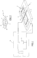
- FIG. 1 represents a power module 1 intended to equip a converter of power on board a railway vehicle, tested according to a method of the art prior art in accordance with IEC 1287-1.
- the power module 1 intended to be tested comprises three power elements 2 electrically mounted in parallel and resting on a metal base 8.
- Each power element 2, shown in isolation and in more detail in FIG. comprises a dielectric substrate 5 on which an IGBT component 3 and a diode 4 associated in parallel, in the opposite position, the diode 4 allowing the reversibility of current in module 1.
- IGBT 3 and diode 4 components are conventionally covered with a dielectric gel.
- Each IGBT component 3 is provided with a collector 10, a transmitter 11, and conventionally comprises a control gate 12 making it possible to in the off state or in the on state the power component 3.
- the grids of 12 of the three IGBT 3 components are interconnected in order to have a common terminal, arranged laterally on the power module 1 shown in Figure 1, controlling the blocked or passing state of the three components IGBT 3.
- test method In the test method according to IEC 1287-1, all the connections of the power module, namely the collectors 10, the emitters 11 and the terminal 12 of the control grids, are interconnected by a first circuit 6. A voltage is then applied, by means of a test device 20, between the first circuit 6 and a second circuit 7 brought into contact with the metal base 8, the device 20 providing, in the example shown, an alternating voltage. The level of discharge is simultaneously measured between the first circuit 6 and the second circuit 7 at the This type of test method has the disadvantage of test only the insulation related to dielectric substrates 5.
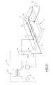
- FIG. 3 shows the power module 1 of FIG. 1 tested according to a mode particular embodiment of the test method according to the invention.
- the collectors 10 of the power module are electrically connected to each other by means of a first circuit 13 which is connected to a first terminal 31 of a test device 30.
- the emitters 11 of the power module 1 are connected electrically to each other by means of a second circuit 14 which is connected to a second terminal 32 of the test device 30, the latter comprising between these two terminal 31, 32 a generator 33 of alternating voltage arranged in series with a generator 34 of DC voltage.
- Voltage values of the voltage generator alternative 33 and the DC generator 34 are such that one has, at each moment, the voltage Vtest between the terminals 31 and 32 which verifies Vtest> 0 so as to test the power module under a variable voltage never negative in order to avoid that the diodes 4 do not pass in natural conduction which would make impossible the measurement of partial discharges.
- DC voltage is applied by means of a generator 15, between the terminal 12 of the control gates and the emitters 11, connected between them by the second circuit 14, so as to put in the off state the components IGBT 3 of the three power elements 2 of module 1. When all these power supply conditions are verified, landfills are measured between the first circuit 13 and the second circuit 14 by means of a classical measurement 21.
- FIG. 4 shows an alternative embodiment of the test device 30 differentiating the device shown in Figure 3 in that, between the terminals 31 and 32, the DC voltage generator 34 is arranged in parallel with the generator 33 of alternating voltage, the generators 33 and 34 being dimensioned in such a way that the voltage Vtest between the terminals 31 and 32 checks at each instant Vtest> 0.
- the device 21 for measuring partial discharges is disposed between the terminal 32 of the test device 30 and the second circuit 14 which is connected to the emitters 11 of the power module. Terminal 31 remains connected directly to the first circuit 13 and the test method remains unchanged from that described in FIG. figure 3.
- Such a test method has the advantage of enabling the detection of discharges partial due to the encapsulation of the power components.
- the method of test according to the invention allows the detection of partial discharges in the gel dielectric, between the emitter welding wires and the collector metallization, between power terminals or at the interface between the different dielectric materials, by example at the bond between the gel and the epoxy resin.
- this test method has the advantage of measuring partial discharges under conditions close to those encountered during the actual use of the power module.
- Such a test method which remains very simple to implement, can advantageously to be used for the follow-up of changes over time of characteristic quantities a power module for predictive maintenance.
Landscapes
- Physics & Mathematics (AREA)
- General Physics & Mathematics (AREA)
- Testing Of Individual Semiconductor Devices (AREA)
- Testing Relating To Insulation (AREA)
- Testing Electric Properties And Detecting Electric Faults (AREA)
- Power Conversion In General (AREA)
Applications Claiming Priority (2)
| Application Number | Priority Date | Filing Date | Title |
|---|---|---|---|
| FR0110388 | 2001-08-02 | ||
| FR0110388A FR2828288B1 (fr) | 2001-08-02 | 2001-08-02 | Procede et dispositif de test d'un module de puissance |
Publications (2)
| Publication Number | Publication Date |
|---|---|
| EP1281978A1 true EP1281978A1 (de) | 2003-02-05 |
| EP1281978B1 EP1281978B1 (de) | 2009-04-15 |
Family
ID=8866234
Family Applications (1)
| Application Number | Title | Priority Date | Filing Date |
|---|---|---|---|
| EP02291688A Expired - Lifetime EP1281978B1 (de) | 2001-08-02 | 2002-07-05 | Verfahren und Vorrichtung zur Prüfung eines Leistungsmoduls |
Country Status (14)
| Country | Link |
|---|---|
| US (1) | US6836125B2 (de) |
| EP (1) | EP1281978B1 (de) |
| JP (1) | JP4249956B2 (de) |
| KR (1) | KR100986928B1 (de) |
| CN (1) | CN1272636C (de) |
| AT (1) | ATE428935T1 (de) |
| AU (1) | AU2002300263B2 (de) |
| CA (1) | CA2396190C (de) |
| DE (1) | DE60231940D1 (de) |
| ES (1) | ES2329661T3 (de) |
| FR (1) | FR2828288B1 (de) |
| HK (1) | HK1052746B (de) |
| RU (1) | RU2298201C2 (de) |
| TW (1) | TWI221205B (de) |
Cited By (1)
| Publication number | Priority date | Publication date | Assignee | Title |
|---|---|---|---|---|
| CN111273105A (zh) * | 2020-03-03 | 2020-06-12 | 海信集团有限公司 | 一种智能家电设备及其供电检测方法 |
Families Citing this family (7)
| Publication number | Priority date | Publication date | Assignee | Title |
|---|---|---|---|---|
| US7486099B1 (en) | 2008-02-28 | 2009-02-03 | Caterpillar Inc. | System and method for testing power transistors |
| US8427331B2 (en) * | 2008-12-31 | 2013-04-23 | Caterpillar Inc. | System and method for testing power transistors |
| US20120039045A1 (en) * | 2009-04-22 | 2012-02-16 | Mitsubishi Electric Corporation | Power module and method for detecting insulation degradation thereof |
| CN102540023B (zh) * | 2011-12-13 | 2017-04-05 | 上海电机系统节能工程技术研究中心有限公司 | 绝缘结构局部放电信号检测装置 |
| FR3116347B1 (fr) | 2020-11-17 | 2022-12-09 | Safran Electrical & Power | Procédé et dispositif de test d’un module de puissance |
| JP7582111B2 (ja) * | 2021-07-29 | 2024-11-13 | トヨタ自動車株式会社 | 電力システムおよび電力算出方法 |
| CN114325062B (zh) * | 2022-03-10 | 2022-06-10 | 杭州飞仕得科技有限公司 | 一种功率模组的电流测试方法 |
Citations (1)
| Publication number | Priority date | Publication date | Assignee | Title |
|---|---|---|---|---|
| US5523620A (en) * | 1994-02-14 | 1996-06-04 | Delco Electronics Corporation | Coplanar linear dual switch module |
Family Cites Families (7)
| Publication number | Priority date | Publication date | Assignee | Title |
|---|---|---|---|---|
| JPH05333089A (ja) * | 1992-06-02 | 1993-12-17 | Toshiba Corp | 大電力半導体素子の試験回路 |
| JPH09162255A (ja) * | 1995-12-06 | 1997-06-20 | Fuji Electric Co Ltd | 半導体素子の試験装置 |
| DE19725836C2 (de) * | 1997-06-18 | 2001-10-04 | Infineon Technologies Ag | Leistungshalbleiter-Anordnung auf DCB-Substrat |
| JPH1114694A (ja) * | 1997-06-20 | 1999-01-22 | Sanmei Denki Kk | パワーモジュールにおけるワイヤボンディング部の耐久性能試験方法 |
| US6054765A (en) * | 1998-04-27 | 2000-04-25 | Delco Electronics Corporation | Parallel dual switch module |
| JP2001013204A (ja) * | 1999-06-29 | 2001-01-19 | Toshiba Corp | パワーデバイス試験装置 |
| US6300878B1 (en) * | 2000-01-13 | 2001-10-09 | Cooper Industries, Inc. | Constant current regulator using IGBT control |
-
2001
- 2001-08-02 FR FR0110388A patent/FR2828288B1/fr not_active Expired - Fee Related
-
2002
- 2002-07-05 AT AT02291688T patent/ATE428935T1/de active
- 2002-07-05 ES ES02291688T patent/ES2329661T3/es not_active Expired - Lifetime
- 2002-07-05 DE DE60231940T patent/DE60231940D1/de not_active Expired - Lifetime
- 2002-07-05 EP EP02291688A patent/EP1281978B1/de not_active Expired - Lifetime
- 2002-07-23 US US10/200,191 patent/US6836125B2/en not_active Expired - Lifetime
- 2002-07-25 AU AU2002300263A patent/AU2002300263B2/en not_active Ceased
- 2002-07-29 KR KR1020020044745A patent/KR100986928B1/ko not_active Expired - Fee Related
- 2002-07-29 TW TW091116907A patent/TWI221205B/zh not_active IP Right Cessation
- 2002-07-30 JP JP2002221359A patent/JP4249956B2/ja not_active Expired - Fee Related
- 2002-07-30 CA CA2396190A patent/CA2396190C/fr not_active Expired - Fee Related
- 2002-08-01 RU RU2002121000/28A patent/RU2298201C2/ru not_active IP Right Cessation
- 2002-08-02 CN CNB021274827A patent/CN1272636C/zh not_active Expired - Fee Related
-
2003
- 2003-07-09 HK HK03104946.4A patent/HK1052746B/zh not_active IP Right Cessation
Patent Citations (1)
| Publication number | Priority date | Publication date | Assignee | Title |
|---|---|---|---|---|
| US5523620A (en) * | 1994-02-14 | 1996-06-04 | Delco Electronics Corporation | Coplanar linear dual switch module |
Cited By (2)
| Publication number | Priority date | Publication date | Assignee | Title |
|---|---|---|---|---|
| CN111273105A (zh) * | 2020-03-03 | 2020-06-12 | 海信集团有限公司 | 一种智能家电设备及其供电检测方法 |
| CN111273105B (zh) * | 2020-03-03 | 2021-12-14 | 海信集团有限公司 | 一种智能家电设备及其供电检测方法 |
Also Published As
| Publication number | Publication date |
|---|---|
| HK1052746B (zh) | 2007-04-20 |
| CA2396190C (fr) | 2010-05-04 |
| CA2396190A1 (fr) | 2003-02-02 |
| US20030025522A1 (en) | 2003-02-06 |
| RU2298201C2 (ru) | 2007-04-27 |
| DE60231940D1 (de) | 2009-05-28 |
| FR2828288A1 (fr) | 2003-02-07 |
| JP4249956B2 (ja) | 2009-04-08 |
| AU2002300263B2 (en) | 2006-12-07 |
| HK1052746A1 (en) | 2003-09-26 |
| ES2329661T3 (es) | 2009-11-30 |
| CN1405571A (zh) | 2003-03-26 |
| KR100986928B1 (ko) | 2010-10-08 |
| US6836125B2 (en) | 2004-12-28 |
| ATE428935T1 (de) | 2009-05-15 |
| EP1281978B1 (de) | 2009-04-15 |
| KR20030011668A (ko) | 2003-02-11 |
| CN1272636C (zh) | 2006-08-30 |
| FR2828288B1 (fr) | 2003-10-24 |
| TWI221205B (en) | 2004-09-21 |
| JP2003130909A (ja) | 2003-05-08 |
Similar Documents
| Publication | Publication Date | Title |
|---|---|---|
| EP1233275B2 (de) | Vorrichtung und Verfahren zum Prüfen von Leiterplatten | |
| US8301409B2 (en) | Photon imaging system for detecting defects in photovoltaic devices, and method thereof | |
| US5248936A (en) | Semiconductor integrated circuit and a method of testing the same | |
| US20050252545A1 (en) | Infrared detection of solar cell defects under forward bias | |
| US4441248A (en) | On-line inspection method and system for bonds made to electronic components | |
| EP1281978B1 (de) | Verfahren und Vorrichtung zur Prüfung eines Leistungsmoduls | |
| US5111137A (en) | Method and apparatus for the detection of leakage current | |
| EP0905776B1 (de) | Halbleiteranordnung mit zwei mit einem Erdungsanschluss verbundenen Erdungsverbindungspunkten und Testverfahren dafür | |
| Xiao et al. | Failure analysis of field‐failed bypass diodes | |
| FR2984011A1 (fr) | Appareil pour le cablage industriel et les tests finaux de modules concentrateurs photovoltaiques | |
| US20220187352A1 (en) | Connection test device and method for checking an intermittent impedance variation | |
| FR2717901A1 (fr) | Dispositif de détection de courant. | |
| EP0495698B1 (de) | Verfahren und Gerät zur Prüfung paralellgeschalteter Dioden mit sichtbaren Übergängen | |
| FR3066605B1 (fr) | Procede applique a un module de puissance d'un onduleur photovoltaique pour obtenir un vieillissement accelere | |
| FR2975500A1 (fr) | Procede et dispositif de controle electrique des soudures de composants electroniques | |
| Ciocia et al. | Quality Check During Manufacturing of Custom Photovoltaic Modules with Back-Contact Cells | |
| FR2697636A1 (fr) | Dispositif pour tests hyperfréquences à large bande réalisés in situ. | |
| Goranti | Potential induced degradation (PID) study of fresh and accelerated stress tested photovoltaic modules | |
| EP1361451A1 (de) | Kontaktor zur Inspektion von mikroelektronischen Anordnungen und Inspektionsvorrichtung mit solchem Kontaktor | |
| CA2087688A1 (fr) | Procede et systeme de test du fonctionnement et/ou de la presence d'elements connectes en parallele | |
| FR2676543A1 (fr) | Dispositif pour tests hyperfrequences a large bande realises in situ. | |
| Li et al. | Lock-in Photoluminescence Imaging for Enhancing In-Situ Detection of Multi-Source Damage in Photovoltaic Modules | |
| FR2873449A1 (fr) | Procede de detection de defauts sur les connexions internes d'un circuit integre et dispositif correspondant | |
| FR2770302A1 (fr) | Procede et dispositif de mesure de tension continue de circuits, par application d'une tension pulsee et par faisceau d'electrons |
Legal Events
| Date | Code | Title | Description |
|---|---|---|---|
| PUAI | Public reference made under article 153(3) epc to a published international application that has entered the european phase |
Free format text: ORIGINAL CODE: 0009012 |
|
| AK | Designated contracting states |
Designated state(s): AT BE BG CH CY CZ DE DK EE ES FI FR GB GR IE IT LI LU MC NL PT SE SK TR |
|
| AX | Request for extension of the european patent |
Extension state: AL LT LV MK RO SI |
|
| 17P | Request for examination filed |
Effective date: 20030805 |
|
| AKX | Designation fees paid |
Designated state(s): AT BE BG CH CY CZ DE DK EE ES FI FR GB GR IE IT LI LU MC NL PT SE SK TR |
|
| RAP1 | Party data changed (applicant data changed or rights of an application transferred) |
Owner name: ALSTOM |
|
| RAP1 | Party data changed (applicant data changed or rights of an application transferred) |
Owner name: ALSTOM TRANSPORT SA |
|
| GRAP | Despatch of communication of intention to grant a patent |
Free format text: ORIGINAL CODE: EPIDOSNIGR1 |
|
| GRAS | Grant fee paid |
Free format text: ORIGINAL CODE: EPIDOSNIGR3 |
|
| GRAA | (expected) grant |
Free format text: ORIGINAL CODE: 0009210 |
|
| AK | Designated contracting states |
Kind code of ref document: B1 Designated state(s): AT BE BG CH CY CZ DE DK EE ES FI FR GB GR IE IT LI LU MC NL PT SE SK TR |
|
| REG | Reference to a national code |
Ref country code: CH Ref legal event code: EP Ref country code: GB Ref legal event code: FG4D Free format text: NOT ENGLISH |
|
| REG | Reference to a national code |
Ref country code: IE Ref legal event code: FG4D |
|
| REF | Corresponds to: |
Ref document number: 60231940 Country of ref document: DE Date of ref document: 20090528 Kind code of ref document: P |
|
| REG | Reference to a national code |
Ref country code: SE Ref legal event code: TRGR |
|
| NLV1 | Nl: lapsed or annulled due to failure to fulfill the requirements of art. 29p and 29m of the patents act | ||
| PG25 | Lapsed in a contracting state [announced via postgrant information from national office to epo] |
Ref country code: FI Free format text: LAPSE BECAUSE OF FAILURE TO SUBMIT A TRANSLATION OF THE DESCRIPTION OR TO PAY THE FEE WITHIN THE PRESCRIBED TIME-LIMIT Effective date: 20090415 Ref country code: PT Free format text: LAPSE BECAUSE OF FAILURE TO SUBMIT A TRANSLATION OF THE DESCRIPTION OR TO PAY THE FEE WITHIN THE PRESCRIBED TIME-LIMIT Effective date: 20090915 |
|
| PG25 | Lapsed in a contracting state [announced via postgrant information from national office to epo] |
Ref country code: NL Free format text: LAPSE BECAUSE OF FAILURE TO SUBMIT A TRANSLATION OF THE DESCRIPTION OR TO PAY THE FEE WITHIN THE PRESCRIBED TIME-LIMIT Effective date: 20090415 |
|
| PGFP | Annual fee paid to national office [announced via postgrant information from national office to epo] |
Ref country code: CH Payment date: 20090715 Year of fee payment: 8 Ref country code: LU Payment date: 20090720 Year of fee payment: 8 |
|
| REG | Reference to a national code |
Ref country code: ES Ref legal event code: FG2A Ref document number: 2329661 Country of ref document: ES Kind code of ref document: T3 |
|
| REG | Reference to a national code |
Ref country code: IE Ref legal event code: FD4D |
|
| PG25 | Lapsed in a contracting state [announced via postgrant information from national office to epo] |
Ref country code: DK Free format text: LAPSE BECAUSE OF NON-PAYMENT OF DUE FEES Effective date: 20090415 |
|
| PG25 | Lapsed in a contracting state [announced via postgrant information from national office to epo] |
Ref country code: IE Free format text: LAPSE BECAUSE OF FAILURE TO SUBMIT A TRANSLATION OF THE DESCRIPTION OR TO PAY THE FEE WITHIN THE PRESCRIBED TIME-LIMIT Effective date: 20090415 Ref country code: EE Free format text: LAPSE BECAUSE OF FAILURE TO SUBMIT A TRANSLATION OF THE DESCRIPTION OR TO PAY THE FEE WITHIN THE PRESCRIBED TIME-LIMIT Effective date: 20090415 Ref country code: CZ Free format text: LAPSE BECAUSE OF FAILURE TO SUBMIT A TRANSLATION OF THE DESCRIPTION OR TO PAY THE FEE WITHIN THE PRESCRIBED TIME-LIMIT Effective date: 20090415 |
|
| PLBE | No opposition filed within time limit |
Free format text: ORIGINAL CODE: 0009261 |
|
| STAA | Information on the status of an ep patent application or granted ep patent |
Free format text: STATUS: NO OPPOSITION FILED WITHIN TIME LIMIT |
|
| PG25 | Lapsed in a contracting state [announced via postgrant information from national office to epo] |
Ref country code: MC Free format text: LAPSE BECAUSE OF NON-PAYMENT OF DUE FEES Effective date: 20090731 Ref country code: SK Free format text: LAPSE BECAUSE OF FAILURE TO SUBMIT A TRANSLATION OF THE DESCRIPTION OR TO PAY THE FEE WITHIN THE PRESCRIBED TIME-LIMIT Effective date: 20090415 |
|
| 26N | No opposition filed |
Effective date: 20100118 |
|
| GBPC | Gb: european patent ceased through non-payment of renewal fee |
Effective date: 20090715 |
|
| PG25 | Lapsed in a contracting state [announced via postgrant information from national office to epo] |
Ref country code: BG Free format text: LAPSE BECAUSE OF FAILURE TO SUBMIT A TRANSLATION OF THE DESCRIPTION OR TO PAY THE FEE WITHIN THE PRESCRIBED TIME-LIMIT Effective date: 20090715 |
|
| REG | Reference to a national code |
Ref country code: FR Ref legal event code: ST Effective date: 20100331 |
|
| PG25 | Lapsed in a contracting state [announced via postgrant information from national office to epo] |
Ref country code: FR Free format text: LAPSE BECAUSE OF NON-PAYMENT OF DUE FEES Effective date: 20090731 |
|
| PG25 | Lapsed in a contracting state [announced via postgrant information from national office to epo] |
Ref country code: GB Free format text: LAPSE BECAUSE OF NON-PAYMENT OF DUE FEES Effective date: 20090715 |
|
| PG25 | Lapsed in a contracting state [announced via postgrant information from national office to epo] |
Ref country code: GR Free format text: LAPSE BECAUSE OF FAILURE TO SUBMIT A TRANSLATION OF THE DESCRIPTION OR TO PAY THE FEE WITHIN THE PRESCRIBED TIME-LIMIT Effective date: 20090716 |
|
| REG | Reference to a national code |
Ref country code: CH Ref legal event code: PL |
|
| PG25 | Lapsed in a contracting state [announced via postgrant information from national office to epo] |
Ref country code: CH Free format text: LAPSE BECAUSE OF NON-PAYMENT OF DUE FEES Effective date: 20100731 Ref country code: LI Free format text: LAPSE BECAUSE OF NON-PAYMENT OF DUE FEES Effective date: 20100731 |
|
| PG25 | Lapsed in a contracting state [announced via postgrant information from national office to epo] |
Ref country code: TR Free format text: LAPSE BECAUSE OF FAILURE TO SUBMIT A TRANSLATION OF THE DESCRIPTION OR TO PAY THE FEE WITHIN THE PRESCRIBED TIME-LIMIT Effective date: 20090415 |
|
| PG25 | Lapsed in a contracting state [announced via postgrant information from national office to epo] |
Ref country code: CY Free format text: LAPSE BECAUSE OF FAILURE TO SUBMIT A TRANSLATION OF THE DESCRIPTION OR TO PAY THE FEE WITHIN THE PRESCRIBED TIME-LIMIT Effective date: 20090415 |
|
| PG25 | Lapsed in a contracting state [announced via postgrant information from national office to epo] |
Ref country code: LU Free format text: LAPSE BECAUSE OF NON-PAYMENT OF DUE FEES Effective date: 20100705 |
|
| REG | Reference to a national code |
Ref country code: DE Ref legal event code: R081 Ref document number: 60231940 Country of ref document: DE Owner name: ALSTOM TRANSPORT TECHNOLOGIES, FR Free format text: FORMER OWNER: ALSTOM TRANSPORT S.A., LEVALLOIS-PERRET, FR |
|
| REG | Reference to a national code |
Ref country code: DE Ref legal event code: R081 Ref document number: 60231940 Country of ref document: DE Owner name: ALSTOM TRANSPORT TECHNOLOGIES, FR Free format text: FORMER OWNER: ALSTOM TRANSPORT TECHNOLOGIES, LEVALLOIS-PERRET, FR |
|
| REG | Reference to a national code |
Ref country code: AT Ref legal event code: PC Ref document number: 428935 Country of ref document: AT Kind code of ref document: T Owner name: ALSTOM TRANSPORT TECHNOLOGIES, FR Effective date: 20180220 |
|
| PGFP | Annual fee paid to national office [announced via postgrant information from national office to epo] |
Ref country code: SE Payment date: 20190719 Year of fee payment: 18 Ref country code: ES Payment date: 20190822 Year of fee payment: 18 Ref country code: IT Payment date: 20190730 Year of fee payment: 18 Ref country code: DE Payment date: 20190719 Year of fee payment: 18 |
|
| PGFP | Annual fee paid to national office [announced via postgrant information from national office to epo] |
Ref country code: BE Payment date: 20190718 Year of fee payment: 18 |
|
| PGFP | Annual fee paid to national office [announced via postgrant information from national office to epo] |
Ref country code: AT Payment date: 20190722 Year of fee payment: 18 |
|
| REG | Reference to a national code |
Ref country code: DE Ref legal event code: R119 Ref document number: 60231940 Country of ref document: DE |
|
| REG | Reference to a national code |
Ref country code: SE Ref legal event code: EUG |
|
| REG | Reference to a national code |
Ref country code: AT Ref legal event code: MM01 Ref document number: 428935 Country of ref document: AT Kind code of ref document: T Effective date: 20200705 |
|
| REG | Reference to a national code |
Ref country code: BE Ref legal event code: MM Effective date: 20200731 |
|
| PG25 | Lapsed in a contracting state [announced via postgrant information from national office to epo] |
Ref country code: DE Free format text: LAPSE BECAUSE OF NON-PAYMENT OF DUE FEES Effective date: 20210202 Ref country code: AT Free format text: LAPSE BECAUSE OF NON-PAYMENT OF DUE FEES Effective date: 20200705 Ref country code: BE Free format text: LAPSE BECAUSE OF NON-PAYMENT OF DUE FEES Effective date: 20200731 Ref country code: SE Free format text: LAPSE BECAUSE OF NON-PAYMENT OF DUE FEES Effective date: 20200706 |
|
| REG | Reference to a national code |
Ref country code: ES Ref legal event code: FD2A Effective date: 20211129 |
|
| PG25 | Lapsed in a contracting state [announced via postgrant information from national office to epo] |
Ref country code: ES Free format text: LAPSE BECAUSE OF NON-PAYMENT OF DUE FEES Effective date: 20200706 |
|
| PG25 | Lapsed in a contracting state [announced via postgrant information from national office to epo] |
Ref country code: IT Free format text: LAPSE BECAUSE OF NON-PAYMENT OF DUE FEES Effective date: 20200705 |