EP1282143A2 - Herstellungsverfahren eines Magnetkörpers, Magnetkörper und Leiterplatte - Google Patents
Herstellungsverfahren eines Magnetkörpers, Magnetkörper und Leiterplatte Download PDFInfo
- Publication number
- EP1282143A2 EP1282143A2 EP02400036A EP02400036A EP1282143A2 EP 1282143 A2 EP1282143 A2 EP 1282143A2 EP 02400036 A EP02400036 A EP 02400036A EP 02400036 A EP02400036 A EP 02400036A EP 1282143 A2 EP1282143 A2 EP 1282143A2
- Authority
- EP
- European Patent Office
- Prior art keywords
- magnetic body
- circuit board
- printed circuit
- magnetic
- mold
- Prior art date
- Legal status (The legal status is an assumption and is not a legal conclusion. Google has not performed a legal analysis and makes no representation as to the accuracy of the status listed.)
- Granted
Links
Images



Classifications
-
- H—ELECTRICITY
- H05—ELECTRIC TECHNIQUES NOT OTHERWISE PROVIDED FOR
- H05K—PRINTED CIRCUITS; CASINGS OR CONSTRUCTIONAL DETAILS OF ELECTRIC APPARATUS; MANUFACTURE OF ASSEMBLAGES OF ELECTRICAL COMPONENTS
- H05K1/00—Printed circuits
- H05K1/16—Printed circuits incorporating printed electric components, e.g. printed resistors, capacitors or inductors
- H05K1/165—Printed circuits incorporating printed electric components, e.g. printed resistors, capacitors or inductors incorporating printed inductors
-
- H—ELECTRICITY
- H01—ELECTRIC ELEMENTS
- H01F—MAGNETS; INDUCTANCES; TRANSFORMERS; SELECTION OF MATERIALS FOR THEIR MAGNETIC PROPERTIES
- H01F17/00—Fixed inductances of the signal type
- H01F17/04—Fixed inductances of the signal type with magnetic core
- H01F17/06—Fixed inductances of the signal type with magnetic core with core substantially closed in itself, e.g. toroid
-
- H—ELECTRICITY
- H01—ELECTRIC ELEMENTS
- H01F—MAGNETS; INDUCTANCES; TRANSFORMERS; SELECTION OF MATERIALS FOR THEIR MAGNETIC PROPERTIES
- H01F41/00—Apparatus or processes specially adapted for manufacturing or assembling magnets, inductances or transformers; Apparatus or processes specially adapted for manufacturing materials characterised by their magnetic properties
- H01F41/02—Apparatus or processes specially adapted for manufacturing or assembling magnets, inductances or transformers; Apparatus or processes specially adapted for manufacturing materials characterised by their magnetic properties for manufacturing cores, coils, or magnets
- H01F41/0206—Manufacturing of magnetic cores by mechanical means
- H01F41/0246—Manufacturing of magnetic circuits by moulding or by pressing powder
-
- H—ELECTRICITY
- H01—ELECTRIC ELEMENTS
- H01F—MAGNETS; INDUCTANCES; TRANSFORMERS; SELECTION OF MATERIALS FOR THEIR MAGNETIC PROPERTIES
- H01F17/00—Fixed inductances of the signal type
- H01F17/0006—Printed inductances
-
- H—ELECTRICITY
- H01—ELECTRIC ELEMENTS
- H01F—MAGNETS; INDUCTANCES; TRANSFORMERS; SELECTION OF MATERIALS FOR THEIR MAGNETIC PROPERTIES
- H01F17/00—Fixed inductances of the signal type
- H01F17/04—Fixed inductances of the signal type with magnetic core
- H01F17/06—Fixed inductances of the signal type with magnetic core with core substantially closed in itself, e.g. toroid
- H01F2017/065—Core mounted around conductor to absorb noise, e.g. EMI filter
-
- H—ELECTRICITY
- H01—ELECTRIC ELEMENTS
- H01F—MAGNETS; INDUCTANCES; TRANSFORMERS; SELECTION OF MATERIALS FOR THEIR MAGNETIC PROPERTIES
- H01F27/00—Details of transformers or inductances, in general
- H01F27/28—Coils; Windings; Conductive connections
- H01F27/2804—Printed windings
-
- H—ELECTRICITY
- H05—ELECTRIC TECHNIQUES NOT OTHERWISE PROVIDED FOR
- H05K—PRINTED CIRCUITS; CASINGS OR CONSTRUCTIONAL DETAILS OF ELECTRIC APPARATUS; MANUFACTURE OF ASSEMBLAGES OF ELECTRICAL COMPONENTS
- H05K1/00—Printed circuits
- H05K1/02—Details
- H05K1/0213—Electrical arrangements not otherwise provided for
- H05K1/0216—Reduction of cross-talk, noise or electromagnetic interference
- H05K1/023—Reduction of cross-talk, noise or electromagnetic interference using auxiliary mounted passive components or auxiliary substances
- H05K1/0233—Filters, inductors or a magnetic substance
-
- H—ELECTRICITY
- H05—ELECTRIC TECHNIQUES NOT OTHERWISE PROVIDED FOR
- H05K—PRINTED CIRCUITS; CASINGS OR CONSTRUCTIONAL DETAILS OF ELECTRIC APPARATUS; MANUFACTURE OF ASSEMBLAGES OF ELECTRICAL COMPONENTS
- H05K2201/00—Indexing scheme relating to printed circuits covered by H05K1/00
- H05K2201/08—Magnetic details
- H05K2201/083—Magnetic materials
- H05K2201/086—Magnetic materials for inductive purposes, e.g. printed inductor with ferrite core
-
- H—ELECTRICITY
- H05—ELECTRIC TECHNIQUES NOT OTHERWISE PROVIDED FOR
- H05K—PRINTED CIRCUITS; CASINGS OR CONSTRUCTIONAL DETAILS OF ELECTRIC APPARATUS; MANUFACTURE OF ASSEMBLAGES OF ELECTRICAL COMPONENTS
- H05K2203/00—Indexing scheme relating to apparatus or processes for manufacturing printed circuits covered by H05K3/00
- H05K2203/13—Moulding and encapsulation; Deposition techniques; Protective layers
- H05K2203/1305—Moulding and encapsulation
- H05K2203/1327—Moulding over PCB locally or completely
-
- Y—GENERAL TAGGING OF NEW TECHNOLOGICAL DEVELOPMENTS; GENERAL TAGGING OF CROSS-SECTIONAL TECHNOLOGIES SPANNING OVER SEVERAL SECTIONS OF THE IPC; TECHNICAL SUBJECTS COVERED BY FORMER USPC CROSS-REFERENCE ART COLLECTIONS [XRACs] AND DIGESTS
- Y10—TECHNICAL SUBJECTS COVERED BY FORMER USPC
- Y10T—TECHNICAL SUBJECTS COVERED BY FORMER US CLASSIFICATION
- Y10T428/00—Stock material or miscellaneous articles
- Y10T428/24—Structurally defined web or sheet [e.g., overall dimension, etc.]
- Y10T428/24802—Discontinuous or differential coating, impregnation or bond [e.g., artwork, printing, retouched photograph, etc.]
- Y10T428/24917—Discontinuous or differential coating, impregnation or bond [e.g., artwork, printing, retouched photograph, etc.] including metal layer
Definitions
- This invention relates to a method of forming a magnetic body, such as a choke or transformer core, on a printed circuit board, the magnetic body, and the printed circuit board on which the magnetic body is formed.
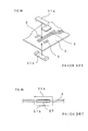
- Fig. 4A shows a conventional method for providing a ferrite core and the like on a printed circuit board, for noise control or for use in transformer and choke coil.
- a ferrite core is formed and split into two pieces in advance.
- the split ferrite core pieces 51a, 51b are then attached to a printed circuit board 3 respectively from both sides and glued to each other via attachment holes 5, 5 created beforehand.
- a ferrite core is typically molded from compacted ferrite material by a sintering molding process, it is difficult to form the core to the desired measurements and shape. Thus, it is necessary to grind the sinter molded ferrite core to the desired dimensions after the core is sintered. Also, if the maximum tolerances of the sintered ferrite core are too great, the distances to adjacent electronic components on a printed circuit board must be at least as great as the tolerances, and this could prevent high density packaging. Moreover, a ferrite core which is made too thin is likely to break or get chipped when dropped or in transit.
- gaps 57 are likely to appear between the respective ferrite core pieces 51a, 51b and a circuit pattern 6 on the printed circuit board 3 as illustrated in Fig. 4B.
- a gap 57 between the circuit pattern 6 and the ferrite core pieces 51a, 51b causes a decline in magnetic properties of the ferrite core, which increases rapidly as the gap 57 increases.
- An object of the present invention is to provide a magnetic body, and a manufacturing method thereof, as an alternative to a ferrite core or similar shape, for noise control and for use in transformers and choke coils.
- the present invention discloses a method of forming a magnetic body by preparing a magnetic material by mixing and melting at least a magnetic filler and a binder containing one or more kinds of resin, setting a printed circuit board in a mold, and injection molding to or around the printed circuit board using the magnetic material, by which the magnetic body is formed to cover a circuit pattern on the printed circuit board.
- the magnetic body includes resin as binder, and is thereby more resistant to shocks than ferrite alone. Owing to injection molding of the body, the molding tolerances are reduced to 10% of that of the case of sintering molding. Accordingly, there is no need to grind the magnetic body after it is formed. Also, it is possible to arrange the magnetic body close to other electronic components which are generally provided on a printed circuit board (including a flexible board). Thus, high density packaging is realized.
- the magnetic body is formed in such a manner that it is appressed to the printed circuit board as a result of the injection molding process.
- the term “appressed” means that a magnetic body 7 is formed as a single, unitary body without unwanted gaps therein or unwanted gaps between the magnetic body and the printed circuit board.
- a gate for supplying the melted material to a cavity of the mold is in the form of pin gate.
- a cross section of the gate becomes small and a trace of the gate on the molded magnetic body is not obtrusive, or clearly distinct. Therefore, the gate can be provided at any desired position even when two magnetic bodies (or a magnetic body and another member) are molded adjacently.
- the printed circuit board has at least one through-hole in an area where the magnetic body is formed, and material is supplied to form the magnetic body on both sides of the printed circuit board via the through-hole.
- the magnetic body is formed on both sides of the printed circuit board at one time, and it is not necessary to use adhesives and the like to hold the magnetic body fast to the printed circuit board.
- the magnetic body is formed to cover an electronic component mounted on the printed circuit board.
- the covered electronic component is protected from noise.
- the electronic component to be covered may be a pin, resistance or condenser. Other electronic components can be covered as well.
- such a magnetic body can function to the full extent, and it does not need be ground after formed.
- the magnetic body may be formed on only one side of the printed circuit board.
- the magnetic body can be set adjacent to other electronic components, and high density packaging can be attained.
- Figs. 1A-1C, 2A and 2B show how a printed circuit board 3 according to the present invention is produced.
- the same reference numbers as those in Figs. 4A and 4B are used to represent the same components, so far as such use of the same numbers does not cause unnecessary confusion.
- a case is described in which a magnetic body for noise control is provided in a position X on the printed circuit board 3 of Fig. 1A.
- attachment holes 5, 5 are created in the printed circuit board 3 in advance.
- the printed circuit board 3 is then set in a mold 11 as shown in Fig. 2A to perform the injection molding process.
- This mold 11 comprises a fixed plate 11a, an intermediate plate 11b and a movable plate 11c.
- a melted material 11d comprised of a magnetic material filler and a binder is filled into a cavity 17b via a sprue 13, a runner 15 and a gate 16.
- Fig. 2B is a sectional view taken along the line B-B in Fig. 2A.
- the cavity 17b on the intermediate plate 11b communicates to a cavity 17c on the movable plate 11c via one or more holes 5 in the printed circuit board 3.
- the material lid supplied to the cavity 17b reaches and fills the cavity 17c through one or more holes 5, 5.
- soft ferrite is used as a magnetic filler
- PolyAmide 12 is used as binder.
- the gate 16, which is an inflow opening which supplies the material to the cavity 17b is in the form of pin gate.
- the gate 16 may be in the form of side gate or submarine gate.
- Fig. 1B shows a portion of the printed circuit board 3 after direct injection molding by which, for example, a magnetic body 7 for noise control is formed on the printed circuit board 3.
- the magnetic body 7 appears similar to conventional ferrite core pieces 51a, 51b.
- Fig. 1C which is a sectional view taken along the line A-A in Fig. 1B, no gap 57 appears in the magnetic body 7 or between the magnetic body 7 and the printed circuit board 3. Consequently, the magnetic body 7 for noise control can function well and without degradation of its magnetic properties.
- FIG. 5A shows the case in which the magnetic body 7 is appressed to the printed circuit board in accordance with the present invention. As shown, a magnetic body mixed resin and ferrite is appressed to and around a measuring cable 21.
- Fig. 5B shows the case in which the magnetic body is not appressed to the printed circuit board according to the present invention and gaps 57 of 0.5 mm are formed between the measuring cable 21 and respective pieces of the magnetic body 23.
- FIG. 5C is a graph showing the result of measurement by impedance analyzer 25 of impedance frequency characteristics in both cases.
- a lateral axis represents frequency and a longitudinal axis represents impedance.
- a full line shows the case of having no gap (Fig. 5A), and a dotted line shows the case of having gaps (Fig. 5B).
- a magnetic body 7 of the present invention is also break resistant since PolyAmide 12 is used as binder. Accordingly, the magnetic body 7 does not easily break or get chipped, unlike the ferrite core pieces 51a, 51b, which break easily.
- the magnetic body 7 is formed as a single, unitary body extending to both sides of the printed circuit board 3, gluing is not necessary, as in the case of ferrite core pieces 51a, 51b.
- the forming tolerance is reduced to 10% of that of the case in using a sintered product, post-forming processing like grinding becomes unnecessary, and thus it is possible to simplify the manufacturing process. By the same reason, the distances to adjacent electronic components can be made smaller, and thus high density packaging can be realized.
- soft ferrite is used for magnetic material.
- other materials such as hard ferrite, amorphous in Fe, Fe-Si, Fe-Si-Al, Fe-Si-Cr, Fe-Ni, Fe-Cr, and Co system, Fe-based nanocrystal can be used.
- the magnetic filler made from such magnetic materials can be formed in any shape, such as round, flat, etc.
- the binder can be thermoplastic resin such as EVA (Ethylene-Vinyl acetate copolymer), EVOH (Ethylene-Vinyl alcohol-Copolymer), PVC (PolyVinylChloride), CPE (Chlorinated polyethylene), CA (Cellulose-Acetate), POM (PolyOxyMethylene), PA (PolyAmide), PAR (Polyarylate), TPU (Thermoplastic Polyurethane), TPE (Thermoplastic-Elastomer), LCP (Liquid Crystal Polymer), PEEK (PolyEtherEtherKetone), PSU (Polysulphone), PES (PolyEtherSulfone), HDPE (High Density Polyethylene), LDPE (Low Density Polyethylene), LLDPE (Linear Low Density Polyethylene), PET (PolyEthylene Terephthalate), PC (PolyCarbonate), PS (PolyStyrene), PPE (E
- a magnetic transformer body 43 may be formed on the printed circuit board 3 on which three attachment holes 41 are created as shown in Fig. 3A.
- the magnetic transformer body 43 having an 8-shaped cross section as shown in Fig. 3C can be formed appressed to the printed circuit board 3.
- a magnetic body 7 for choke coil may be formed on the printed circuit board 3. It is also possible to form a magnetic body 7 only on one side of the printed circuit board 3.
- the circuit pattern 6 can be a signal line, power line, ground line, transformer circuit pattern or choke coil pattern.
Landscapes
- Engineering & Computer Science (AREA)
- Power Engineering (AREA)
- Microelectronics & Electronic Packaging (AREA)
- Manufacturing & Machinery (AREA)
- Coils Or Transformers For Communication (AREA)
- Shielding Devices Or Components To Electric Or Magnetic Fields (AREA)
- Injection Moulding Of Plastics Or The Like (AREA)
- Structures For Mounting Electric Components On Printed Circuit Boards (AREA)
- Soft Magnetic Materials (AREA)
Applications Claiming Priority (2)
| Application Number | Priority Date | Filing Date | Title |
|---|---|---|---|
| JP2001233559A JP4638626B2 (ja) | 2001-08-01 | 2001-08-01 | 磁性体の成形方法、磁性体、およびプリント基板 |
| JP2001233559 | 2001-08-01 |
Publications (3)
| Publication Number | Publication Date |
|---|---|
| EP1282143A2 true EP1282143A2 (de) | 2003-02-05 |
| EP1282143A3 EP1282143A3 (de) | 2003-04-02 |
| EP1282143B1 EP1282143B1 (de) | 2010-04-14 |
Family
ID=19065320
Family Applications (1)
| Application Number | Title | Priority Date | Filing Date |
|---|---|---|---|
| EP02400036A Expired - Lifetime EP1282143B1 (de) | 2001-08-01 | 2002-07-29 | Herstellungsverfahren eines Magnetkörpers, Magnetkörper und Leiterplatte |
Country Status (4)
| Country | Link |
|---|---|
| US (2) | US6758999B2 (de) |
| EP (1) | EP1282143B1 (de) |
| JP (1) | JP4638626B2 (de) |
| DE (1) | DE60235941D1 (de) |
Cited By (4)
| Publication number | Priority date | Publication date | Assignee | Title |
|---|---|---|---|---|
| WO2005024862A1 (en) * | 2003-09-04 | 2005-03-17 | Philips Intellectual Property & Standards Gmbh | Fractional turns transformers with ferrite polymer core |
| WO2013110726A1 (fr) * | 2012-01-24 | 2013-08-01 | Valeo Systèmes d'Essuyage | Filtre atténuateur/éliminateur de bande des inductions électromagnétiques pour moteur à courant continu à balais |
| WO2014096049A1 (de) * | 2012-12-18 | 2014-06-26 | Phoenix Contact Gmbh & Co. Kg | Verfahren zur herstellung eines magnetisch leitenden kreises |
| CN105895308A (zh) * | 2016-06-24 | 2016-08-24 | 国家电网公司 | 带漏孔的定位碗及其成型方法 |
Families Citing this family (37)
| Publication number | Priority date | Publication date | Assignee | Title |
|---|---|---|---|---|
| US8097926B2 (en) | 2008-10-07 | 2012-01-17 | Mc10, Inc. | Systems, methods, and devices having stretchable integrated circuitry for sensing and delivering therapy |
| US9545216B2 (en) | 2011-08-05 | 2017-01-17 | Mc10, Inc. | Catheter balloon methods and apparatus employing sensing elements |
| US8389862B2 (en) | 2008-10-07 | 2013-03-05 | Mc10, Inc. | Extremely stretchable electronics |
| US9123614B2 (en) | 2008-10-07 | 2015-09-01 | Mc10, Inc. | Methods and applications of non-planar imaging arrays |
| JP5646492B2 (ja) | 2008-10-07 | 2014-12-24 | エムシー10 インコーポレイテッドMc10,Inc. | 伸縮可能な集積回路およびセンサアレイを有する装置 |
| WO2011041727A1 (en) | 2009-10-01 | 2011-04-07 | Mc10, Inc. | Protective cases with integrated electronics |
| JP5255592B2 (ja) * | 2010-04-15 | 2013-08-07 | 古河電気工業株式会社 | 基板 |
| JP5170908B2 (ja) * | 2010-04-20 | 2013-03-27 | 古河電気工業株式会社 | 基板および基板の製造方法 |
| KR102000302B1 (ko) | 2011-05-27 | 2019-07-15 | 엠씨10, 인크 | 전자, 광학, 및/또는 기계 장치 및 시스템, 그리고 이를 제조하기 위한 방법 |
| US9226402B2 (en) | 2012-06-11 | 2015-12-29 | Mc10, Inc. | Strain isolation structures for stretchable electronics |
| US9295842B2 (en) | 2012-07-05 | 2016-03-29 | Mc10, Inc. | Catheter or guidewire device including flow sensing and use thereof |
| KR20150031324A (ko) | 2012-07-05 | 2015-03-23 | 엠씨10, 인크 | 유동 감지를 포함하는 카테터 장치 |
| US9171794B2 (en) | 2012-10-09 | 2015-10-27 | Mc10, Inc. | Embedding thin chips in polymer |
| WO2014058473A1 (en) | 2012-10-09 | 2014-04-17 | Mc10, Inc. | Conformal electronics integrated with apparel |
| US9706647B2 (en) | 2013-05-14 | 2017-07-11 | Mc10, Inc. | Conformal electronics including nested serpentine interconnects |
| JP2016527649A (ja) | 2013-08-05 | 2016-09-08 | エムシー10 インコーポレイテッドMc10,Inc. | 適合する電子機器を含む可撓性温度センサ |
| US10467926B2 (en) | 2013-10-07 | 2019-11-05 | Mc10, Inc. | Conformal sensor systems for sensing and analysis |
| JP6711750B2 (ja) | 2013-11-22 | 2020-06-17 | エムシー10 インコーポレイテッドMc10,Inc. | 心臓活動の検知および分析のためのコンフォーマルセンサシステム |
| CA2935372C (en) | 2014-01-06 | 2023-08-08 | Mc10, Inc. | Encapsulated conformal electronic systems and devices, and methods of making and using the same |
| US10485118B2 (en) | 2014-03-04 | 2019-11-19 | Mc10, Inc. | Multi-part flexible encapsulation housing for electronic devices and methods of making the same |
| US9899330B2 (en) | 2014-10-03 | 2018-02-20 | Mc10, Inc. | Flexible electronic circuits with embedded integrated circuit die |
| US10297572B2 (en) | 2014-10-06 | 2019-05-21 | Mc10, Inc. | Discrete flexible interconnects for modules of integrated circuits |
| USD781270S1 (en) | 2014-10-15 | 2017-03-14 | Mc10, Inc. | Electronic device having antenna |
| US10085654B2 (en) | 2014-11-07 | 2018-10-02 | Welch Allyn, Inc. | Medical device |
| WO2016134306A1 (en) | 2015-02-20 | 2016-08-25 | Mc10, Inc. | Automated detection and configuration of wearable devices based on on-body status, location, and/or orientation |
| WO2016140961A1 (en) | 2015-03-02 | 2016-09-09 | Mc10, Inc. | Perspiration sensor |
| US10653332B2 (en) | 2015-07-17 | 2020-05-19 | Mc10, Inc. | Conductive stiffener, method of making a conductive stiffener, and conductive adhesive and encapsulation layers |
| US10709384B2 (en) | 2015-08-19 | 2020-07-14 | Mc10, Inc. | Wearable heat flux devices and methods of use |
| US10300371B2 (en) | 2015-10-01 | 2019-05-28 | Mc10, Inc. | Method and system for interacting with a virtual environment |
| CN108289630A (zh) | 2015-10-05 | 2018-07-17 | Mc10股份有限公司 | 用于神经调节和刺激的方法和系统 |
| WO2017147053A1 (en) | 2016-02-22 | 2017-08-31 | Mc10, Inc. | System, device, and method for coupled hub and sensor node on-body acquisition of sensor information |
| US10277386B2 (en) | 2016-02-22 | 2019-04-30 | Mc10, Inc. | System, devices, and method for on-body data and power transmission |
| CN109310340A (zh) | 2016-04-19 | 2019-02-05 | Mc10股份有限公司 | 用于测量汗液的方法和系统 |
| US10447347B2 (en) | 2016-08-12 | 2019-10-15 | Mc10, Inc. | Wireless charger and high speed data off-loader |
| CN106799812A (zh) * | 2016-12-21 | 2017-06-06 | 维沃移动通信有限公司 | 一种usb装置的加工方法、usb装置和移动终端 |
| JP7109979B2 (ja) * | 2018-04-26 | 2022-08-01 | 矢崎総業株式会社 | 基板 |
| KR102884631B1 (ko) | 2019-12-11 | 2025-11-12 | 엘지이노텍 주식회사 | 인쇄회로기판 모듈 |
Citations (2)
| Publication number | Priority date | Publication date | Assignee | Title |
|---|---|---|---|---|
| US3650023A (en) | 1969-08-08 | 1972-03-21 | Bell Telephone Labor Inc | Method for fabricating ferrite core plug-in devices |
| JPH0697610A (ja) | 1992-09-14 | 1994-04-08 | Fuji Xerox Co Ltd | プリント配線板 |
Family Cites Families (22)
| Publication number | Priority date | Publication date | Assignee | Title |
|---|---|---|---|---|
| CH359171A (de) | 1958-03-28 | 1961-12-31 | Gustav Dipl Ing Guanella | Hochfrequenzübertrager |
| US4935174A (en) * | 1986-01-13 | 1990-06-19 | Canon Kabushiki Kaisha | Resin molded article bearing electric circuit patterns and process for producing the same |
| JPH01165415A (ja) * | 1987-12-22 | 1989-06-29 | Mitsubishi Cable Ind Ltd | Icカードケースの製造方法 |
| US4898759A (en) * | 1988-07-27 | 1990-02-06 | Nidec Corporation | Molded printed circuit board for use with a brushless electric motor |
| US5047283A (en) * | 1989-09-20 | 1991-09-10 | Ppg Industries, Inc. | Electrically conductive article |
| JPH03183516A (ja) * | 1989-12-14 | 1991-08-09 | Furukawa Electric Co Ltd:The | 導電層付き成形体の製造方法 |
| JPH0494586A (ja) * | 1990-08-10 | 1992-03-26 | Mitsubishi Electric Corp | プリント基板 |
| JPH04101405A (ja) * | 1990-08-20 | 1992-04-02 | West Electric Co Ltd | 薄型トランス及びその製造方法 |
| JP2844584B2 (ja) * | 1991-09-24 | 1999-01-06 | 日立電線株式会社 | 電磁シールドされた回路基板 |
| CA2080177C (en) * | 1992-01-02 | 1997-02-25 | Edward Allan Highum | Electro-magnetic shield and method for making the same |
| KR0127666B1 (ko) * | 1992-11-25 | 1997-12-30 | 모리시다 요이찌 | 세라믹전자부품 및 그 제조방법 |
| US6261508B1 (en) * | 1994-04-01 | 2001-07-17 | Maxwell Electronic Components Group, Inc. | Method for making a shielding composition |
| US5851644A (en) * | 1995-08-01 | 1998-12-22 | Loctite (Ireland) Limited | Films and coatings having anisotropic conductive pathways therein |
| US6200508B1 (en) * | 1996-10-25 | 2001-03-13 | Massachusetts Institute Of Technology | Method of fabricating electro-mechanical devices by multilayer deposition |
| JPH1140224A (ja) * | 1997-07-11 | 1999-02-12 | Jsr Corp | 異方導電性シート |
| US5938979A (en) * | 1997-10-31 | 1999-08-17 | Nanogram Corporation | Electromagnetic shielding |
| JPH11186786A (ja) * | 1997-12-22 | 1999-07-09 | Polyplastics Co | 電磁波シールド成形品及びその製造方法 |
| JPH11214592A (ja) * | 1998-01-21 | 1999-08-06 | Hitachi Ltd | 半導体装置および電子装置 |
| JP3318654B2 (ja) * | 1998-09-04 | 2002-08-26 | 株式会社村田製作所 | ビーズインダクタの製造方法及び製造装置 |
| JP2001111289A (ja) * | 1999-10-13 | 2001-04-20 | Kyocera Corp | 電波吸収体及びその製造方法 |
| JP2001135525A (ja) * | 1999-11-05 | 2001-05-18 | Tdk Corp | ノイズ対策部品 |
| US6410847B1 (en) * | 2000-07-25 | 2002-06-25 | Trw Inc. | Packaged electronic system having selectively plated microwave absorbing cover |
-
2001
- 2001-08-01 JP JP2001233559A patent/JP4638626B2/ja not_active Expired - Lifetime
-
2002
- 2002-07-29 DE DE60235941T patent/DE60235941D1/de not_active Expired - Lifetime
- 2002-07-29 EP EP02400036A patent/EP1282143B1/de not_active Expired - Lifetime
- 2002-07-30 US US10/209,394 patent/US6758999B2/en not_active Expired - Fee Related
-
2004
- 2004-04-23 US US10/831,428 patent/US20040201134A1/en not_active Abandoned
Patent Citations (2)
| Publication number | Priority date | Publication date | Assignee | Title |
|---|---|---|---|---|
| US3650023A (en) | 1969-08-08 | 1972-03-21 | Bell Telephone Labor Inc | Method for fabricating ferrite core plug-in devices |
| JPH0697610A (ja) | 1992-09-14 | 1994-04-08 | Fuji Xerox Co Ltd | プリント配線板 |
Cited By (7)
| Publication number | Priority date | Publication date | Assignee | Title |
|---|---|---|---|---|
| WO2005024862A1 (en) * | 2003-09-04 | 2005-03-17 | Philips Intellectual Property & Standards Gmbh | Fractional turns transformers with ferrite polymer core |
| US7915991B2 (en) | 2003-09-04 | 2011-03-29 | Koninklijke Philips Electronics N.V. | Fractional turns transformers with ferrite polymer core |
| KR101049757B1 (ko) * | 2003-09-04 | 2011-07-19 | 코닌클리즈케 필립스 일렉트로닉스 엔.브이. | 페라이트 중합체 코어를 갖는 분수 권수 변압기 |
| WO2013110726A1 (fr) * | 2012-01-24 | 2013-08-01 | Valeo Systèmes d'Essuyage | Filtre atténuateur/éliminateur de bande des inductions électromagnétiques pour moteur à courant continu à balais |
| WO2014096049A1 (de) * | 2012-12-18 | 2014-06-26 | Phoenix Contact Gmbh & Co. Kg | Verfahren zur herstellung eines magnetisch leitenden kreises |
| CN105895308A (zh) * | 2016-06-24 | 2016-08-24 | 国家电网公司 | 带漏孔的定位碗及其成型方法 |
| CN105895308B (zh) * | 2016-06-24 | 2017-09-19 | 国家电网公司 | 带漏孔的定位碗及其成型方法 |
Also Published As
| Publication number | Publication date |
|---|---|
| JP4638626B2 (ja) | 2011-02-23 |
| DE60235941D1 (de) | 2010-05-27 |
| EP1282143A3 (de) | 2003-04-02 |
| EP1282143B1 (de) | 2010-04-14 |
| US20030026962A1 (en) | 2003-02-06 |
| US20040201134A1 (en) | 2004-10-14 |
| JP2003046291A (ja) | 2003-02-14 |
| US6758999B2 (en) | 2004-07-06 |
Similar Documents
| Publication | Publication Date | Title |
|---|---|---|
| EP1282143B1 (de) | Herstellungsverfahren eines Magnetkörpers, Magnetkörper und Leiterplatte | |
| EP1640893B1 (de) | Antenne für RFID Etikett | |
| EP1745527B1 (de) | Antennenanordnung zur induktiven energieübertragung und verwendung der antennenanordnung | |
| EP2071667B1 (de) | Antenne und funkgesteuerte Uhr, tastenloses Eingabesystem und RFID-System damit | |
| JP4763609B2 (ja) | 磁性コア部品の製造方法 | |
| EP2416446A1 (de) | Verbund-hf-etikett und mit dem verbund-hf-etikett ausgestattetes werkzeug | |
| US7030828B2 (en) | Coil antenna | |
| EP2190681A2 (de) | Sensoranordnung und verfahren zum betrieb einer sensoranordnung | |
| DE102006024247A1 (de) | Drahtlose Kartentyp-Vorrichtung, Antennenspule und Verfahren zum Herstellen eines Kommunikationsmoduls | |
| EP0986073B1 (de) | Transformatorkern mit getrennten teilen | |
| US7234234B2 (en) | Method of manufacturing bandpass filters for GHz bands | |
| KR102488005B1 (ko) | 밀리미터파 차폐 및 흡수용 복합소재 | |
| WO2012019694A1 (de) | Tragbarer datenträger mit über spulenkopplung arbeitender datenkommunikationseinrichtung | |
| EP0822512B1 (de) | Kontaktlose Chipkarte sowie Verfahren zur Herstellung kontaktloser Chipkarten | |
| AU2020100991A4 (en) | Improved density tracer | |
| EP1592085A1 (de) | Spulenantenne | |
| US20250132647A1 (en) | Magnet unit and method for manufacturing the same | |
| JP4651474B2 (ja) | コイルアンテナ装置 | |
| DE102009023150A1 (de) | Schutzstruktur für einen Funkschlüssel eines Fahrzeugs | |
| JP2003217744A (ja) | 電磁波吸収コネクター | |
| KR20220157740A (ko) | 이동 수단용 무선 충전 장치 및 이에 사용되는 자성 복합체 | |
| DE10353990A1 (de) | Induktiver Näherungssensor |
Legal Events
| Date | Code | Title | Description |
|---|---|---|---|
| PUAI | Public reference made under article 153(3) epc to a published international application that has entered the european phase |
Free format text: ORIGINAL CODE: 0009012 |
|
| 17P | Request for examination filed |
Effective date: 20020729 |
|
| AK | Designated contracting states |
Designated state(s): AT BE BG CH CY CZ DE DK EE ES FI FR GB GR IE IT LI LU MC NL PT SE SK TR |
|
| AX | Request for extension of the european patent |
Extension state: AL LT LV MK RO SI |
|
| PUAL | Search report despatched |
Free format text: ORIGINAL CODE: 0009013 |
|
| AK | Designated contracting states |
Kind code of ref document: A3 Designated state(s): AT BE BG CH CY CZ DE DK EE ES FI FR GB GR IE IT LI LU MC NL PT SE SK TR |
|
| AX | Request for extension of the european patent |
Extension state: AL LT LV MK RO SI |
|
| RIC1 | Information provided on ipc code assigned before grant |
Ipc: 7H 01F 41/02 A Ipc: 7H 01F 17/06 B |
|
| AKX | Designation fees paid |
Designated state(s): DE GB |
|
| 17Q | First examination report despatched |
Effective date: 20090702 |
|
| GRAP | Despatch of communication of intention to grant a patent |
Free format text: ORIGINAL CODE: EPIDOSNIGR1 |
|
| GRAS | Grant fee paid |
Free format text: ORIGINAL CODE: EPIDOSNIGR3 |
|
| GRAA | (expected) grant |
Free format text: ORIGINAL CODE: 0009210 |
|
| AK | Designated contracting states |
Kind code of ref document: B1 Designated state(s): DE GB |
|
| REG | Reference to a national code |
Ref country code: GB Ref legal event code: FG4D |
|
| REF | Corresponds to: |
Ref document number: 60235941 Country of ref document: DE Date of ref document: 20100527 Kind code of ref document: P |
|
| PLBE | No opposition filed within time limit |
Free format text: ORIGINAL CODE: 0009261 |
|
| STAA | Information on the status of an ep patent application or granted ep patent |
Free format text: STATUS: NO OPPOSITION FILED WITHIN TIME LIMIT |
|
| 26N | No opposition filed |
Effective date: 20110117 |
|
| PGFP | Annual fee paid to national office [announced via postgrant information from national office to epo] |
Ref country code: DE Payment date: 20130612 Year of fee payment: 12 |
|
| PGFP | Annual fee paid to national office [announced via postgrant information from national office to epo] |
Ref country code: GB Payment date: 20130710 Year of fee payment: 12 |
|
| REG | Reference to a national code |
Ref country code: DE Ref legal event code: R082 Ref document number: 60235941 Country of ref document: DE Representative=s name: PATENTANWAELTE MAGENBAUER & KOLLEGEN, DE |
|
| REG | Reference to a national code |
Ref country code: DE Ref legal event code: R082 Ref document number: 60235941 Country of ref document: DE Representative=s name: PATENTANWAELTE MAGENBAUER & KOLLEGEN, DE Effective date: 20140613 Ref country code: DE Ref legal event code: R081 Ref document number: 60235941 Country of ref document: DE Owner name: KITAGAWA INDUSTRIES CO., LTD., INAZAWA-SHI, JP Free format text: FORMER OWNER: KITAGAWA INDUSTRIES CO., LTD., NAGOYA, AICHI, JP Effective date: 20140613 Ref country code: DE Ref legal event code: R082 Ref document number: 60235941 Country of ref document: DE Representative=s name: PATENTANWAELTE MAGENBAUER & KOLLEGEN PARTNERSC, DE Effective date: 20140613 |
|
| REG | Reference to a national code |
Ref country code: DE Ref legal event code: R119 Ref document number: 60235941 Country of ref document: DE |
|
| GBPC | Gb: european patent ceased through non-payment of renewal fee |
Effective date: 20140729 |
|
| PG25 | Lapsed in a contracting state [announced via postgrant information from national office to epo] |
Ref country code: DE Free format text: LAPSE BECAUSE OF NON-PAYMENT OF DUE FEES Effective date: 20150203 |
|
| REG | Reference to a national code |
Ref country code: DE Ref legal event code: R119 Ref document number: 60235941 Country of ref document: DE Effective date: 20150203 |
|
| PG25 | Lapsed in a contracting state [announced via postgrant information from national office to epo] |
Ref country code: GB Free format text: LAPSE BECAUSE OF NON-PAYMENT OF DUE FEES Effective date: 20140729 |