EP1282157A2 - Dispositif et procédé de régulation de la temperature d'un substrat - Google Patents
Dispositif et procédé de régulation de la temperature d'un substrat Download PDFInfo
- Publication number
- EP1282157A2 EP1282157A2 EP02255150A EP02255150A EP1282157A2 EP 1282157 A2 EP1282157 A2 EP 1282157A2 EP 02255150 A EP02255150 A EP 02255150A EP 02255150 A EP02255150 A EP 02255150A EP 1282157 A2 EP1282157 A2 EP 1282157A2
- Authority
- EP
- European Patent Office
- Prior art keywords
- substrate
- chamber
- chuck
- temperature
- wafer
- Prior art date
- Legal status (The legal status is an assumption and is not a legal conclusion. Google has not performed a legal analysis and makes no representation as to the accuracy of the status listed.)
- Withdrawn
Links
Images




Classifications
-
- H—ELECTRICITY
- H10—SEMICONDUCTOR DEVICES; ELECTRIC SOLID-STATE DEVICES NOT OTHERWISE PROVIDED FOR
- H10P—GENERIC PROCESSES OR APPARATUS FOR THE MANUFACTURE OR TREATMENT OF DEVICES COVERED BY CLASS H10
- H10P72/00—Handling or holding of wafers, substrates or devices during manufacture or treatment thereof
- H10P72/06—Apparatus for monitoring, sorting, marking, testing or measuring
- H10P72/0602—Temperature monitoring
-
- G—PHYSICS
- G03—PHOTOGRAPHY; CINEMATOGRAPHY; ANALOGOUS TECHNIQUES USING WAVES OTHER THAN OPTICAL WAVES; ELECTROGRAPHY; HOLOGRAPHY
- G03F—PHOTOMECHANICAL PRODUCTION OF TEXTURED OR PATTERNED SURFACES, e.g. FOR PRINTING, FOR PROCESSING OF SEMICONDUCTOR DEVICES; MATERIALS THEREFOR; ORIGINALS THEREFOR; APPARATUS SPECIALLY ADAPTED THEREFOR
- G03F7/00—Photomechanical, e.g. photolithographic, production of textured or patterned surfaces, e.g. printing surfaces; Materials therefor, e.g. comprising photoresists; Apparatus specially adapted therefor
- G03F7/70—Microphotolithographic exposure; Apparatus therefor
- G03F7/70691—Handling of masks or workpieces
- G03F7/70733—Handling masks and workpieces, e.g. exchange of workpiece or mask, transport of workpiece or mask
- G03F7/7075—Handling workpieces outside exposure position, e.g. SMIF box
-
- G—PHYSICS
- G03—PHOTOGRAPHY; CINEMATOGRAPHY; ANALOGOUS TECHNIQUES USING WAVES OTHER THAN OPTICAL WAVES; ELECTROGRAPHY; HOLOGRAPHY
- G03F—PHOTOMECHANICAL PRODUCTION OF TEXTURED OR PATTERNED SURFACES, e.g. FOR PRINTING, FOR PROCESSING OF SEMICONDUCTOR DEVICES; MATERIALS THEREFOR; ORIGINALS THEREFOR; APPARATUS SPECIALLY ADAPTED THEREFOR
- G03F7/00—Photomechanical, e.g. photolithographic, production of textured or patterned surfaces, e.g. printing surfaces; Materials therefor, e.g. comprising photoresists; Apparatus specially adapted therefor
- G03F7/70—Microphotolithographic exposure; Apparatus therefor
- G03F7/708—Construction of apparatus, e.g. environment aspects, hygiene aspects or materials
- G03F7/70808—Construction details, e.g. housing, load-lock, seals or windows for passing light in or out of apparatus
-
- H—ELECTRICITY
- H10—SEMICONDUCTOR DEVICES; ELECTRIC SOLID-STATE DEVICES NOT OTHERWISE PROVIDED FOR
- H10P—GENERIC PROCESSES OR APPARATUS FOR THE MANUFACTURE OR TREATMENT OF DEVICES COVERED BY CLASS H10
- H10P72/00—Handling or holding of wafers, substrates or devices during manufacture or treatment thereof
- H10P72/04—Apparatus for manufacture or treatment
- H10P72/0431—Apparatus for thermal treatment
- H10P72/0432—Apparatus for thermal treatment mainly by conduction
Definitions
- the present invention relates to a substrate processing apparatus and substrate control method and, for example, to a substrate processing apparatus and a substrate processing method suitable for a manufacturing process of a device such as a semiconductor device or liquid crystal display device.
- the wavelength of exposure light used in exposure must be shorten for micropatterning.
- the wavelength has been shortened from a g-line and i-line to a KrF laser beam, ArF laser beam, F 2 laser beam, soft X-ray radiated from an SR ring, or the like.
- the exposure light with a short wavelength, such as the F 2 laser beam or soft X-ray is greatly attenuated in the air.
- the exposure unit of an exposure apparatus is stored in a chamber, wherein N 2 atmosphere or Ppressure-reduced He atmosphere providing small attenuation of the exposure light is formed or a vacuum atmosphere is formed for an electron beam exposure apparatus and the like.
- N 2 atmosphere or Ppressure-reduced He atmosphere providing small attenuation of the exposure light is formed
- a vacuum atmosphere is formed for an electron beam exposure apparatus and the like.
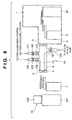
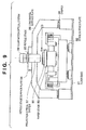
- the substrate processing apparatus of this type includes a process chamber 1 serving as the first chamber which stores a process station for, e.g., exposing the substrate in the atmosphere different from the air, and a substrate supply portion 10 arranged in the air.
- the substrate supply portion 10 includes a substrate carrier support portion 101, on which a carrier 102 storing the substrate is placed manually or by an automatic transfer apparatus.
- a load-lock chamber 3 serving as a second process chamber is arranged.
- a plurality of load-lock chambers 3 may be arranged for loading/unloading.
- the pressure-reduced He atmosphere is formed in the process chamber 1 which stores the processing unit.
- the load-lock chamber 3 has a first gate valve 4 on the air side to shield the load-lock chamber 3 from the substrate supply portion 10 in the air, and a second gate valve 5 on the process chamber 1 side to shield the load-lock chamber 3 from the process chamber 1.
- the load-lock chamber 3 also has an exhaust mechanism 12 for exhausting gas from the load-lock chamber 3, an He gas supply portion 13 for supplying He gas into the load-lock chamber 3, and an N 2 gas supply portion 14 for supplying N 2 gas into the load-lock chamber 3.
- the load-lock chamber 3 includes a substrate holding chuck 6 designed to store, e.g., one or a plurality of substrates.
- a first transfer mechanism 7 for transferring the substrate between the substrate carrier 102 on the carrier support portion 101 and the load-lock chamber 3 is arranged.
- a second transfer mechanism 8 for transferring the substrate between the load-lock chamber 3 and a process station (exposure process portion) 20 is arranged.
- the first transfer mechanism 7 extracts one substrate from the substrate carrier 102 placed on the carrier support portion 101, and transfers the substrate to the load-lock chamber 3.
- the first gate valve When the substrate is loaded into the load-lock chamber 3 and placed on the substrate holding chuck 6, the first gate valve is closed to shield the load-lock chamber 3 from the air. The atmosphere in the load-lock chamber 3 is purged.
- Purging the atmosphere in the load-lock chamber 3 is performed to be described below.
- a vacuum exhaust valve 122 is opened in a state wherein the load-lock chamber 3 is shielded from the air and the chamber 1 by closing the first and second gate valves 4 and 5. The gas is then exhausted from the load-lock chamber 3 by a vacuum exhaust pump (not shown) via a vacuum exhaust pipe 121.
- the chamber is evacuated to a predetermined vacuum degree. After evacuating the chamber to the predetermined vacuum degree, the vacuum exhaust valve 122 is closed, and the evacuation is stopped.
- the gas supply valve is then opened.
- the load-lock chamber 3 shown in Fig. 8 includes an He gas supply valve 132 and N 2 gas supply valve 142. At this stage, the He gas supply valve 132 of these supply valves is opened to supply the same gas as the atmosphere in the chamber 1 storing the process station (exposure process portion) 20.
- the He gas is supplied.
- the He gas supply valve 132 is closed to stop supplying the He gas.
- the second gate valve 5 When supply of the He gas is stopped, the second gate valve 5 is opened. The substrate on the substrate holding chuck 6 is extracted by the second transfer mechanism 8 in the preliminary chamber 2, and transferred to the process station (exposure process portion) 20 in the process chamber 1.
- the substrate processed in the process station (exposure process portion) 20 is returned to the substrate carrier 102 via the load-lock chamber 3 by the first and second transfer mechanisms 7 and 8.
- the substrate and substrate holding chuck 6 in the load-lock chamber 3 are exposed to the gas in the load-lock chamber 3, their temperatures are reduced along with cooling the gas.
- the substrate cooled by the adiabatic expansion in the load-lock chamber 3 is loaded into the process chamber 1 and processed at the end of purging the atmosphere.
- the substrate temperature needs to be controlled with high precision in order to obtain high transfer precision, the high line-width precision, and the like.
- the temperature of the substrate loaded into the process chamber 1 via the load-lock chamber 3 is reduced as described above.
- the transfer precision deteriorates when exposure is performed for the wafer in this state, thus posing a problem.
- thermoregulation by the ambient gas is not expected.
- the substrate is thermally regulated by only contact with the substrate transfer means . This requires a longer period of time for which the substrate reaches the predetermined temperature.
- An embodiment of the present invention seeks to provide a substrate processing apparatus which prevents an decrease in throughput due to an decrease in temperature of a substrate along with a reduction in pressure in a load-rock chamber, a substrate controlling method, and an exposure apparatus.
- the first aspect of the present invention is related to a substrate processing apparatus.
- the substrate processing apparatus comprises a first chamber, a second chamber which has a first valve and a second valve, and communicates with the first chamber through said second valve, a thermoregulator which regulates a temperature of the substrate arranged in the second chamber, and a controller which controls a time for which the thermoregulator regulates the temperature of the substrate.
- a substrate transferred to the second chamber through the first valve is temporally held in the second chamber, and then transferred to the first chamber through the second valve.
- thermoregulator heats the substrate.
- the apparatus further comprises a pressure reduction section which reduces a pressure in the second chamber, and the pressure reduction sectioin makes a relationship between the pressure in the second chamber and a pressure reduction time for which the pressure in the second chamber is reduced fall within a predetermined range.
- the apparatus further comprises a gas supply portion which supplies a predetermined gas into the second chamber.
- thermoregulator is arranged in a chuck for holding the substrate, the chuck inluding an electrostatic chuck.
- thermoregulator is arranged in a chuck for holding the substrate, the chuck being controled to have substantially a constant power to chuck the substrate.
- thermoregulator is arranged in a chuck, and the apparatus further comprises a driving section which separates the substrate from the chuck.
- the controller controls the driving section so as to make a time for which the substrate is held by the chuck constant.
- thermoregulator regulates a temperature of the chuck to be higher than a temperature at which the substrate is to be processed in the first chamber.
- the apparatus further comprises a transfer section which transfers the substrate, the thermoregulator is arranged in a chuck, and the controller controls the transfer section so as to make a time for which the substrate is held by the chuck constant.
- thermoregulator regulates a temperature of the chuck to be higher than a temperature at which the substrate is to be processed in the first chamber.
- the second aspect of the present invention is related to a substrate processing method.
- the method includes the steps of regulating a temperature of a substrate in a load-rock chamber, controlling a time for which the temperature of the substrate are regulated in the load-rock chamber, transferring the substrate from the load-rock chamber to a process chamber, and processing the substrate in the process chamber.
- the third aspect of the present invention is related to a device manufacturing method.
- the method comprises the steps of installing, in a device manufacturing factory, manufacturing apparatuses for various processes including the substrate processing apparatus defined in claim 1 and manufacturing a device by a plurality of processes using the manufacturing apparatuses.
- the method further comprises the steps of connecting the manufacturing apparatuses via a local area network, and communicating information about at least one of the manufacturing apparatuses between the local area network and an external network outside the device manufacturing factory.
- the method further comprises the step of accessing a database provided by a vendor or user of the substrate processing apparatus via the external network, thereby obtaining maintenance information of the exposure apparatus by data communication.
- the method further comprises the step of performing data communication between the device manufacturing factory and another device manufacturing factory via the external network, thereby performing production management.
- the fourth aspect of the present invention is related to a device manufacturing factory.
- the device manufacturing factory comprises manufacturing apparatuses for various processes including the substrate processing apparatus defined in claim 1, a local area network for connecting the manufacturing apparatuses, and a gateway for allowing access to the local area network and an external network outside the device manufacturing factory, wherein information about at least one of the manufacturing apparatuses can be communicated between the local area network and the external network.
- the fifth aspect of the present invention is related to a maintenance method of the substrate processing apparatus defined in claim 1 and installed in the device manufacturing factory.
- the method comprises the steps of making a vendor or user of the substrate processing apparatus provide a maintenance database connected to an external network outside the device manufacturing factory, allowing access to the maintenance database from the device manufacturing factory via the external network, and transmitting maintenance information accumulated in the maintenance database to the device manufacturing factory via the external network.
- the above substrate processing apparatus preferably further comprises a display, a network interface, and a computer for executing network software, and maintenance information of the substrate processing apparatus can be communicated via a computer network.
- Fig. 1 is a plan view showing an arrangement of a substrate processing apparatus according to a preferred embodiment of the present invention
- Fig. 2 is an elevation of the apparatus.
- the substrate processing apparatus comprises a process chamber 1 serving as the first process chamber and a substrate supply portion 10 arranged in the air.
- the process chamber 1 is arranged as an exposure apparatus having an internal space in which an exposure process portion 20 for transferring a pattern to a substrate is arranged and a pressure-reduced He atmosphere is maintained.
- the substrate supply portion 10 has a substrate carrier support portion 101, on which a substrate carrier 102 storing a substrate (wafer) W is placed manually or by an automatic transfer apparatus.
- a preliminary chamber 2 which contains a second transfer mechanism 8 is connected to the process chamber 1.
- a load-lock chamber 3 serving as the second chamber is arranged between the process chamber 1 and the substrate supply portion 10.
- the load-lock chamber 3 includes a first gate valve 4 on the air side to shield the load-lock chamber 3 from the substrate supply portion 10 in the air (external environment), and a second gate valve 5 on the chamber side to shield the load-lock chamber 3 from the preliminary chamber 2.
- the load-lock chamber 3 also includes a manometer 31 for measuring a pressure in the load-rock chamber 3, an exhaust mechanism 12 for exhausting gas from the load-lock chamber 3, and gas supply portions for supplying gas to the load-rock chamber 3.
- a manometer 31 for measuring a pressure in the load-rock chamber 3
- an exhaust mechanism 12 for exhausting gas from the load-lock chamber 3
- gas supply portions for supplying gas to the load-rock chamber 3.
- an He gas supply portion 13 for supplying He gas and an N 2 gas supply portion 14 for supplying N 2 gas are arranged as one example of the gas supply portions.
- the exhaust mechanism 12 has a vacuum exhaust pump (not shown), a vacuum supply pipe 121 for connecting the vacuum exhaust pump and the load-rock chamber 3, and a vacuum exhaust valve 122 for regulating the flow rate of gas flowing to the vacuum exhaust pump through an exhaust port.
- the exhaust mechanism 12 is also has a flowmeter 123 for measuring the flow rate of gas flowing in the vacuum exhaust tube 121.
- the gas supply portions have the same structure.
- the He gas supply portion 13 has a supply pipe 131 for connecting the He gas supply portion 13 to the load-rock chamber 3, a gas supply valve 132 for controlling supply of gas flowing in the supply pipe 131, and a gas supply flowmeter 134 for measuring the flow rate of gas flowing between the gas supply valve 132 and load-rock chamber 3.
- the N 2 gas supply portion 14 has a supply pipe 141 for connecting the N 2 gas supply portion 14 to the load-rock chamber 3, a gas supply valve 142 for controlling supply of gas flowing in the supply pipe 141, and a gas supply flowmeter 144 for measuring the flow rate of gas flowing between the gas supply valve 142 and load-rock chamber 3.
- Particles are removed by a filter 133 from the supply gas supplied from the He gas supply portion 13 through the gas supply valve 132 and gas supply flowmeter 134, and the cleaned gas is supplied to the process chamber 1 through the load-rock chamber 3.
- particles are removed by a filter 143 from the supply gas supplied from the N 2 gas supply portion 14 through the gas supply valve 142 and gas supply flowmeter 144, and the cleaned is supplied to the process chamber 1 through the load-rock chamber 3.
- the load-rock chamber 3 has a substrate holding chuck 6 designed, e.g., to store one or a plurality of substrates.
- the substrate holding chuck 6 is an electrostatic suction chuck which attracts a substrate by applying a voltage from a power source (not shown) .
- the substrate holding chuck 6 has a voltmeter (not shown) which indicates an applied voltage.
- Figs. 3A and 3B are views showing the substrate holding chuck 6 in this embodiment.
- the substrate holding chuck 6 has an internal electrode 61 and a heating element 62 which forms a thermoregulator.
- a heating element 62 for example, a heater may be used.
- the substrate holding chuck 6 has a temperature sensor (not shown) which measures temperatures of the substrate holding chuck 6 and provides measurement results to the controller of the heating element 62.
- the substrate holding chuck 6 is further has a driving section which lifts the substrate (wafer) W.
- the driving section may be formed by, e.g., three pins 63 shown in Fig. 3A, but the present invention is not limited to this.
- the driving section may have an arbitrary structure as far as it can lift the substrate (wafer) W.
- the load-rock chamber 3, the first transfer mechanism 7 for transferring a substrate, and the second transfer mechanism 8 are arranged to transfer the substrates one by one.
- the internal volume of the load-rock chamber 3 is preferably set to a minimum size.
- a first transfer mechanism 7 for transferring the substrate (wafer) W between the substrate carrier 102 on the substrate carrier support portion 101 and the load-lock chamber 3 is arranged in the air.
- the second transfer mechanism 8 for transferring the substrate (wafer) W between the load-lock chamber 3 and process station (exposure process portion) 20 is arranged in the preliminary chamber 2 connected between the process chamber 1 and the load-lock chamber 3.
- the three pins 63 lift the wafer W.
- the substrate holding hand of the first or second transfer mechanism 7 or 8 is inserted in a gap between the substrate holding chuck 6 and the wafer W lifted by the three pins 63.
- the substrate holding hand lifts the substrate (wafer) W to separate it from the three pins 63 of the chuck 6.
- the first or second transfer mechanism 7 or 8 transfers the substrate (wafer) W separated from the three pins 63 of the chuck 6.
- the first and second transfer mechanisms 7 and 8 transfer the substrate (wafer) W in a horizontal direction in this embodiment, but the present invention does not limited to this.
- the first and second transfer mechanism 7 and 8 may transfer the substrate (wafer) W in an arbitrary direction, e.g., a vertical direction.
- the arm of the first transfer mechanism 7 is inserted in the substrate carrier 102 in the air, and a single substrate (wafer) W is extracted by this arm.
- the first transfer mechanism 7 holds the substrate (wafer) W while bending its arm. Meanwhile, the pressure gauge 31 measures the state of the atmosphere in the load-lock chamber 3.
- the first transfer mechanism 7 rotates its arm toward the load-rock chamber 3, and after confirming the opening state of the first gate valve 4, the first transfer mechanism 7 stretches its arm toward the substrate (wafer) W to load it into the load-rock chamber 3.
- the substrate (wafer) W is placed on the three pins 63 of the substrate holding chuck 6.
- the three pins 63 of the substrate holding chuck 6 move downward to attract and held the substrate (wafer) W by the substrate holding chuck 6.
- thermoregulator starts thermal regulation to the wafer W from a timing when the wafer W is attracted and held by the substrate holding chuck 6.
- a controller 30 manages the time from a timing when the thermoregulator starts the thermal regulation to the wafer W.
- the first gate valve 4 is closed, and the air is purged with He.
- a time from when the substrate (wafer) W is hold by the substrate holding chuck 6 until the first evacuation for atmosphere purging is started is a predetermined time.
- the air is exhausted to a vacuum first.
- the vacuum exhaust pump (not shown) is always operated. This always keeps vacuum a region from the vacuum exhaust pump to the vacuum exhaust valve 122.
- an experiment is conducted in advance to obtain a curve representing the relationship between a pressure in the load-rock chamber 3 and a pressure reduction time (vacuum suction time) for which a pressure in the load-rock chamber 3 is reduced by the vacuum exhaust pump (not shown), and the experiment resultant is prepared as data.
- the relationship between a vacuum suction time and a pressure in the load-rock chamber 3 has been monitored by the exhaust gas flowmeter 123 and the pressure gauge 31 of the load-rock chamber 3.
- the opening degree of the exhaust valve 122 is controlled such that the relationship falls within the predetermined range.
- the predetermined range is set narrower than an allowable value in the curve representing the relationship between a pressure and a vacuum suction time decided from the adiabatic cooling of the substrate (wafer) W.
- the relationship between a vacuum suction time and pressure is controlled such that it does not exceed the allowable value of the curve representing the relationship between the predetermined vacuum suction time and pressure.
- the relationship between a pressure in the load-rock chamber 3 and a vacuum suction time can also be monitored by using the pressure gauge 31 of the load-rock chamber 3 and the elapse of time.
- the vacuum exhaust valve 122 After evacuating the load-rock chamber 3 to reach the measurement value of a pressure therein measured by the pressure gauge 31 of the load-rock chamber 3 to a predetermined value, the vacuum exhaust valve 122 is closed, and the operation of drawing to a vacuum in the load-rock chamber 3 ends.
- the pressure value in the load-rock chamber 3 becomes the predetermined pressure value, the evacuation ends. Consequently, a time from the start to the end of the evacuation is constant every time.
- gas in the load-rock chamber 3 is cooled by adiabatic expansion, and the substrate (wafer) W in contact with the cooled gas is similarly cooled.
- the temperatures of the device and the plurality of substrates (wafers) W before the evacuation operation are constant.
- the temperature of the cooled substrate (wafer) W is uniformly controlled.
- the gas supply valve is then opened.
- the load-rock chamber 3 in Fig. 2 has the He gas supply valve 132 and N 2 gas supply valve 142 serving as the gas supply valves.
- a gas supply valve which is opened in this case is a gas supply valve for supplying the same gas as the atmosphere in the process chamber 1, which is the He gas supply valve 132.
- the He gas supply portion 13 supplies He gas until a pressure in the load-rock chamber 3 equals that in the process chamber 1.
- the He gas supply valve 132 is closed, and supply of the He gas is stopped.
- the flow rate of the supply gas supplied from the He gas supply portion 13 is measured by the gas supply flowmeter 134.
- the gas supply flowmeter 134 is so controlled as to end supply of gas within a predetermined time.
- the predetermined time is preferably decided in advance on the basis of the relationship between a flow rate and the volume of the load-rock chamber 3.
- the gas supply valves 132 and 142 may be controlled on the basis of the measurement values of the gas supply flowmeters 134 and 144 so as to end supply of gas within a predetermined time.
- the second gate valve 5 After stopping supply of the He gas, the second gate valve 5 is opened, and the second transfer mechanism 8 of the preliminary chamber 2 extracts the substrate (wafer) W in the load-rock chamber 3 to transfer it to the process station (exposure process portion) 20.
- the controller 30 controls a thermal regulating time by the substrate holding chuck 6 so as to make constant a time for which the substrate (wafer) W is held on a holding portion (substrate holding chuck 6).
- the controller 30 controls the three pins 63 of the chuck to lift the substrate (wafer) W.
- the chuck 6 ends the thermal regulation to the substrate (wafer) W.
- the second transfer mechanism 8 then receives the substrate (wafer) W.
- the chuck 6 is preferably an electrostatic chuck. This makes a suction force for the substrate (wafer) W constant regardless of the ambient pressure if an apply voltage to an internal electrode is set constant.
- an apply voltage to the internal electrode is measured by the voltmeter (not shown) and kept constant.
- the contact thermal resistance between the substrate holding chuck 6 and substrate (wafer) W is made constant.
- the chuck 6 is similarly cooled by the adiabatic expansion of gas in the load-rock chamber 3, but the thermoregulator (heater) can keep the temperatures of the substrate (wafer) W and substrate holding chuck 6 constant on the basis of a measurement result from the temperature sensor (not shown) formed in the chuck 6.
- the temperature of the chuck 6 is kept at an appropriate temperature in advance, even when the substrate (wafer) W is cooled, an decrease in temperature of the substrate (wafer) W can be recovered by heating the chuck 6 to a temperature higher than the decrease in temperature.
- the temperature of the substrate (wafer) W is thus kept constant at high precision.
- a temperature t1 of the chuck 6 is set at, e.g., the same temperature as a predetermined temperature at which the substrate (wafer) W is to be processed in the process chamber 1.
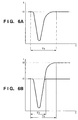
- a change in temperature of the substrate (wafer) W represents the curve shown in Fig. 6A.
- a temperature t of the substrate (wafer) W comes close gradually to a predetermined temperature at which the substrate (wafer) W is to be processed in the process chamber 1 (e.g., t1). That is, the temperature t of the substrate (wafer) W becomes stable in the range of the predetermined temperature after a time T1.
- the temperature of the chuck 6 can be set at a temperature t2 higher than the temperature t1 at which the substrate (wafer) W is to be processed in the process chamber 1 (e.g., 30°C is set with respect to the processing temperature of 23°C).
- a change in temperature of the substrate (wafer) W represents the curve shown in Fig. 6B.
- the temperature of the substrate (wafer) W gradually increases after the elapse of a time T3, and is then close gradually to the temperature t2 of the chuck 6.
- the controller 30 controls the chuck 6 to lift the substrate (wafer) W by its three pins 63 and to end thermal regulation operation for the substrate (wafer) W.
- the controller 30 controls the chuck 6 to stop thermal regulation to the substrate (wafer) W when the time T3 has elapsed, thereby making the temperature of the substrate (wafer) W at a predetermined temperature at which the substrate (wafer) W is to be processed by the process chamber 1.
- the controller 30 can control the chuck 6 to lift the substrate (wafer) W by its three pins 63, and control the transfer mechanism to transfer the substrate (wafer) W.
- the chuck 6 is preferably a good heat conductor such as copper.
- an electrostatic suction chuck is preferably used as the chuck 6.
- the electrostatic suction chuck has a characteristic in that its suction force is constant regardless of the pressure of the ambient gas.
- the vacuum suction chuck 6 shown in Figs. 4A and 4B has a vacuum suction groove 65 along a concentric circle to vacuum-chuck and hold the substrate (wafer) W.
- the substrate holding chuck 6 in the load-rock chamber 3 preferably has a pin-chuck structure.
- thermal transfer from the chuck 6 to the substrate (wafer) W similarly occurs through contact portions.
- the ambient gas of the pins is exhausted along with evacuation, and the time T3 depends on a decrease in thermal transfer along with a decrease in pressure of the ambient gas of the pins and the length of time for which the wafer is held by the chuck 6, thereby controlling the time T3 to be constant as described above.
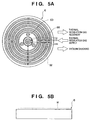
- thermoregulator used as a heating means is not limited to the afore-mentioned heater, and may have a structure so as to flow a fluid such as a thermal-regulated gas or liquid in holes 66 for circulation formed along a plurality of concentric circles in the chuck 6, as shown in Figs. 5A and 5B.
- the preferred embodiment of the present invention represents an example of controlling all the parameters to become constant, but is not limited to this.
- a parameter which is to reach a predetermined value without any control and the like may not be controlled.
- all parameters are controlled to become constant.
- the present invention is not limited to this, and at least one parameter may be so controlled as to become constant.
- the parameter which is to become constant in a predetermined range without any control a parameter which hardly affects any processing for the substrate (wafer) W and need not be controlled, and the like may not be controlled.
- the atmosphere of a process chamber 1 which is the first chamber having a process station (exposure process portion) 20 which performs exposure and the like is a vacuum atmosphere.
- a load-rock chamber 3 according to the present embodiment to purge the atmosphere between the process chamber 1 and a substrate supply portion 10 in the air is formed, and a preliminary chamber 2 is formed between the load-rock chamber 3 and process chamber 1.
- a second transfer mechanism 8 for transferring a substrate between the load-rock chamber 3 and process station (exposure process portion) 20 is formed in the preliminary chamber 2.
- the transfer hand of the second transfer mechanism 8 is so formed as to make an area in contact with a substrate (wafer) W minimum.
- the transfer hand of the second transfer mechanism 8 supports the lower surface of the substrate (wafer) W by one or a plurality of pins and opposes the side surfaces of the substrate to grippers or wall members which are spaced them at an appropriate gap so as to prevent the substrate from moving in the transfer hand during the transfer.
- These grippers or walls may have a pin shape, which minimizes an area in contact with the substrate.
- the transfer hand of the second transfer mechanism 8 has three or more conical pins, each of which has a sloping portion on its side surface abutting against the side surface of the substrate (wafer) W, and the remaining portion not in contact with the substrate.
- the contact area of the second transfer mechanism 8 and substrate (wafer) W is preferably made small as described above.
- the substrate (wafer) W unloaded from the load-rock chamber 3 is transferred to the process station (exposure process portion) 20 while keeping the temperature of the substrate (wafer) W almost constant.
- the temperature of the substrate (wafer) W falls within a predetermined temperature range at a timing when the substrate is unloaded from the load-rock chamber 3 by the second transfer mechanism 8.
- the substrate (wafer) W transferred to the process station (exposure process portion) 20 already has a temperature which falls within the range of a predetermined temperature at which the substrate (wafer) W is to be processed in the process chamber. This requires no thermal regulation in the process station (exposure process portion), so that exposure processing can be immediately started, thereby increasing the throughput.
- FIG. 9 is a front view showing an example of the main structure of the scanning exposure apparatus main body according to the preferred embodiment of the present invention.
- This exposure apparatus main body is arranged in the above process chamber serving as the first process chamber, and performs exposure for a substrate (wafer).
- a lens barrel surface plate 96 is supported by a floor/base 91 via a damper 98.
- the lens barrel surface plate 96 supports a reticle stage surface plate 94, and also supports a projection optical system 97 arranged between a reticle stage 95 and a wafer stage 93.
- the wafer stage 93 having a chuck 90 is supported on a stage surface plate 92 arranged on the floor/base 91, and holds the substrate (wafer) set on the chuck 90 to position the substrate (wafer).
- the reticle stage 95 is supported on the reticle stage surface plate 94 supported by the lens barrel surface plate 96, and can move while mounting the reticle serving as a master on which a circuit pattern is formed. Exposure light for exposing the reticle mounted on the reticle stage 95 onto the substrate (wafer) on the wafer stage 93 is emitted from an illumination optical system 99.
- the wafer stage 93 is scanned in synchronism with the reticle stage 95.
- the positions of both stages are continuously detected by interferometers, respectively, and the detection results are fed back to driving units of the reticle stage 95 and wafer stage 93.
- the scanning start positions of both the stages can be accurately synchronized, and the scanning speed in a constant-speed scanning region can be controlled with high precision.
- both the stages scan the projection optical system 97, the reticle pattern is exposed on the substrate (wafer), and the circuit pattern is transferred.
- a production system for a semiconductor device (semiconductor chip such as an IC or LSI, a liquid crystal panel, a CCD, a thin-film magnetic head, a micromachine, or the like) using an apparatus according to the present invention will be exemplified.
- the system performs maintenance services such as trouble shooting, periodic maintenance, and software distribution for manufacturing apparatuses installed in a semiconductor manufacturing factory by utilizing a computer network or the like outside the manufacturing factory.
- Fig. 10 shows the overall system cut out at a given angle.
- reference numeral 1101 denotes an office of a vendor (apparatus supply manufacturer) which provides a semiconductor device manufacturing apparatus.
- the manufacturing apparatus are semiconductor manufacturing apparatuses for various processes used in a semiconductor manufacturing factory, such as pre-process apparatuses (lithography apparatus including an exposure apparatus, resist processing apparatus, and etching apparatus, an annealing apparatus, a film formation apparatus, a planarization apparatus, and the like) and post-process apparatuses (assembly apparatus, inspection apparatus, and the like) .
- the office 1101 comprises a host management system 1108 which provides a maintenance database for the manufacturing apparatus, a plurality of operation terminal computers 1110, and a LAN (Local Area Network) 1109 which connects the host management system 1108 and computers 1110 to build an intranet or the like.
- the host management system 1108 has a gateway for connecting the LAN 1109 to Internet 1105 serving as an external network of the office, and a security function for limiting external accesses.
- Reference numerals 1102 to 1104 denote manufacturing factories of the semiconductor manufacturer as users of manufacturing apparatuses.
- the manufacturing factories 1102 to 1104 may belong to different manufacturers or the same manufacturer (pre-process factory, post-process factory, and the like).
- Each of the factories 1102 to 1104 is equipped with a plurality of manufacturing apparatuses 1106, a LAN (Local Area Network) 1111 which connects these apparatuses 1106 to construct an intranet, and a host management system 1107 serving as a monitoring apparatus which monitors the operation status of each manufacturing apparatus 1106.
- the host management system 1107 in each of the factories 1102 to 1104 has a gateway for connecting the LAN 1111 in the factory to the Internet 1105 serving as an external network of the factory.
- Each factory can access the host management system 1108 of the office 1101 of vendor from the LAN 1111 via the Internet 1105.
- the security function of the host management system 1108 authorizes access of only a limited user. More specifically, the factory can notify the vendor via the Internet 1105 of status information (e.g., the symptom of a manufacturing apparatus in trouble) representing the operation status of each manufacturing apparatus 1106. Also, the factory can receive, from the vendor, response information (e.g., information designating a remedy against the trouble, or remedy software or data) corresponding to the notification, or maintenance information such as the latest software or help information.
- TCP/IP communication protocol
- a high-security dedicated network (e.g., ISDN) which inhibits access of a third party can be adopted.
- the host management system is not limited to the one provided by the vendor.
- the user may construct a database and set the database on an external network, and the host management system may authorize access to the database from a plurality of user factories.
- Fig. 11 is a view showing the concept of the overall system of this embodiment that is cut out at a different angle from Fig. 10.
- a plurality of user factories having manufacturing apparatuses and the management system of the manufacturing apparatus vendor are connected via an external network, and production management of each factory or information about at least one manufacturing apparatus is communicated via the external network.
- a factory having manufacturing apparatuses provided by a plurality of vendors and the management systems of the vendors for these manufacturing apparatuses are connected via the external network of the factory, and maintenance information of each manufacturing apparatus is communicated.
- reference numeral 1201 denotes a manufacturing factory of a manufacturing apparatus user (semiconductor device manufacturer).
- Manufacturing apparatuses for various processes e.g., an exposure apparatus 1202, resist processing apparatus 1203, and film formation apparatus 1204 are installed in the manufacturing line of the factory.
- Fig. 11 shows only one manufacturing factory 1201, but a plurality of factories are networked in practice.
- the respective apparatuses in the factory are connected to each other by a LAN 1206 to build an intranet, and a host management system 1205 manages the operation of the manufacturing line.
- the offices of vendors such as an exposure apparatus manufacturer 1210, resist processing apparatus manufacturer 1220, and film formation apparatus manufacturer 1230 comprise host management systems 1211, 1221, and 1231 for executing remote maintenance for the supplied apparatuses.
- Each host management system has a maintenance database and a gateway for an external network, as described above.
- the host management system 1205 for managing the apparatuses in the manufacturing factory of the user, and the management systems 1211, 1221, and 1231 of the vendors for the respective apparatuses are connected via the Internet or dedicated network serving as an external network 1200.
- the operation of the manufacturing line stops. This trouble can be quickly solved by remote maintenance from the vendor of the apparatus in trouble via the Internet 1200. This can minimize the stop of the manufacturing line .
- Each manufacturing apparatus in the semiconductor manufacturing factory comprises a display, a network interface, and a computer which executes network access software and apparatus operating software which are stored in a storage device.
- the storage device is a built-in memory, hard disk, or network file server.
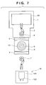
- the network access software includes a dedicated or general-purpose web browser, and provides a user interface with a window as shown in Fig. 12 on the display. While referring to this window, the operator who manages manufacturing apparatuses in each factory inputs, into input fields on the windows, pieces of information such as the model of manufacturing apparatus 1401, serial number 1402, subject of trouble 1403, data of occurrence of trouble 1404, degree of urgency 1405, symptom 1406, remedy 1407, and progress 1408.
- the pieces of input information are transmitted to the maintenance database via the Internet, and appropriate maintenance information is sent back from the maintenance database and provided on the display.
- the user interface provided by the web browser realizes hyperlink functions 1410 to 1412, as shown in Fig. 12. This allows the operator to access more detailed information of each item, download the latest-version software to be used for a manufacturing apparatus from a software library provided by a vendor, and download an operation guide (help information) as a reference for the operator in the factory.
- the maintenance information provided from the maintenance database includes information about the present invention described above.
- the software library also provides the latest-version software for implementing the present invention.
- Fig. 13 shows the flow of the whole manufacturing process of the semiconductor device.
- step 1 circuit design
- step 2 mask formation
- step 3 wafer formation
- step 3 wafer formation
- step 4 wafer process
- an actual circuit is formed on the substrate (wafer) by lithography using the prepared mask and substrate (wafer).
- Step 5 (assembly) called a post-process is the step of forming a semiconductor chip by using the substrate (wafer) formed in step 4, and includes an assembly process (dicing and bonding) and packaging process (chip encapsulation).
- step 6 the semiconductor device manufactured in step 5 undergoes inspections such as an operation confirmation test and durability test. After these steps, the semiconductor device is completed and shipped (step 7).
- the pre-process and post-process are performed in separate dedicated factories, and each of the factories receives maintenance by the above-described remote maintenance system. Information for production management and apparatus maintenance is communicated between the pre-process factory and the post-process factory via the Internet or dedicated network.
- Fig. 14 shows the detailed flow of the wafer process.
- step 11 oxidation
- step 12 CVD
- step 13 electrode formation
- step 14 ion implantation
- step 15 resist processing
- step 16 exposure
- the above-mentioned exposure apparatus exposes the substrate (wafer) to the circuit pattern of a mask, and prints the circuit pattern on the substrate (wafer).
- step 17 developing
- step 18 etching
- step 19 resist removal
- step 19 resist removal
- the substrate (wafer) loaded into the apparatus via the load-lock chamber reaches the predetermined temperature at the time of loading, the substrate (wafer) can be immediately processed, e.g., subjected to exposure, thereby improving the throughput.
- the larger effect can be attained in the apparatus with the evacuated chamber.
Landscapes
- Physics & Mathematics (AREA)
- General Physics & Mathematics (AREA)
- Health & Medical Sciences (AREA)
- Engineering & Computer Science (AREA)
- Environmental & Geological Engineering (AREA)
- Epidemiology (AREA)
- Public Health (AREA)
- Exposure And Positioning Against Photoresist Photosensitive Materials (AREA)
- Container, Conveyance, Adherence, Positioning, Of Wafer (AREA)
- Exposure Of Semiconductors, Excluding Electron Or Ion Beam Exposure (AREA)
Applications Claiming Priority (2)
| Application Number | Priority Date | Filing Date | Title |
|---|---|---|---|
| JP2001227549 | 2001-07-27 | ||
| JP2001227549A JP2003045947A (ja) | 2001-07-27 | 2001-07-27 | 基板処理装置及び露光装置 |
Publications (2)
| Publication Number | Publication Date |
|---|---|
| EP1282157A2 true EP1282157A2 (fr) | 2003-02-05 |
| EP1282157A3 EP1282157A3 (fr) | 2004-03-31 |
Family
ID=19060192
Family Applications (1)
| Application Number | Title | Priority Date | Filing Date |
|---|---|---|---|
| EP02255150A Withdrawn EP1282157A3 (fr) | 2001-07-27 | 2002-07-23 | Dispositif et procédé de régulation de la temperature d'un substrat |
Country Status (3)
| Country | Link |
|---|---|
| US (2) | US7024266B2 (fr) |
| EP (1) | EP1282157A3 (fr) |
| JP (1) | JP2003045947A (fr) |
Cited By (9)
| Publication number | Priority date | Publication date | Assignee | Title |
|---|---|---|---|---|
| EP1457829A1 (fr) * | 2003-03-11 | 2004-09-15 | ASML Netherlands B.V. | Assemblage de projection lithographique, appareil et système pour la manipulation de substrats |
| EP1457830A3 (fr) * | 2003-03-11 | 2005-07-20 | ASML Netherlands B.V. | Appareil lithographique comprenant un sas de chargement conditionné thermiquement |
| EP1455233A3 (fr) * | 2003-03-07 | 2006-02-22 | Canon Kabushiki Kaisha | Méthode et système de traitement |
| EP1653283A3 (fr) * | 2004-10-26 | 2006-07-05 | ASML Netherlands BV | Appareil de lithographie et méthode de fabrication d'un dispositif |
| US7123349B2 (en) | 2003-03-11 | 2006-10-17 | Asml Netherlands B.V. | Lithographic projection assembly, substrate handling apparatus and substrate handling method |
| US7394520B2 (en) | 2003-03-11 | 2008-07-01 | Asml Netherlands B.V. | Temperature conditioned load lock, lithographic apparatus comprising such a load lock and method of manufacturing a substrate with such a load lock |
| US7576831B2 (en) | 2003-03-11 | 2009-08-18 | Asml Netherlands B.V. | Method and apparatus for maintaining a machine part |
| EP1732105A3 (fr) * | 2005-06-06 | 2009-10-28 | Tokyo Electron Limited | Appareil supportant un substrat, et appareil et méthode de contrôle de température d'un substrat |
| US7878755B2 (en) | 2003-03-11 | 2011-02-01 | Asml Netherlands B.V. | Load lock and method for transferring objects |
Families Citing this family (28)
| Publication number | Priority date | Publication date | Assignee | Title |
|---|---|---|---|---|
| JP2003271218A (ja) * | 2002-03-15 | 2003-09-26 | Toshiba Corp | 半導体製造装置、半導体製造システム及び基板処理方法 |
| US8116889B2 (en) | 2002-06-27 | 2012-02-14 | Openpeak Inc. | Method, system, and computer program product for managing controlled residential or non-residential environments |
| JP2004282002A (ja) * | 2003-02-27 | 2004-10-07 | Tokyo Electron Ltd | 基板処理装置及び基板処理方法 |
| JP4468021B2 (ja) | 2003-03-25 | 2010-05-26 | キヤノン株式会社 | ロードロックシステム及び露光処理システム並びにデバイスの製造方法 |
| JP4478440B2 (ja) | 2003-12-02 | 2010-06-09 | キヤノン株式会社 | ロードロック装置および方法 |
| JP4564742B2 (ja) | 2003-12-03 | 2010-10-20 | キヤノン株式会社 | 露光装置及びデバイス製造方法 |
| US20060201074A1 (en) * | 2004-06-02 | 2006-09-14 | Shinichi Kurita | Electronic device manufacturing chamber and methods of forming the same |
| CN103199039B (zh) * | 2004-06-02 | 2016-01-13 | 应用材料公司 | 电子装置制造室及其形成方法 |
| US7151589B2 (en) * | 2004-06-24 | 2006-12-19 | Asml Netherlands B.V. | Lithographic apparatus and patterning device transport |
| JP2006128206A (ja) * | 2004-10-26 | 2006-05-18 | Nikon Corp | 露光方法及び露光装置 |
| KR100629377B1 (ko) | 2005-02-01 | 2006-09-29 | 삼성전자주식회사 | 웨이퍼 하면의 파티클을 감지하는 웨이퍼 처리 방법 및 장치 |
| JP2006245257A (ja) * | 2005-03-03 | 2006-09-14 | Canon Inc | 処理装置、当該処理装置を有する露光装置、保護機構 |
| US20070166134A1 (en) * | 2005-12-20 | 2007-07-19 | Motoko Suzuki | Substrate transfer method, substrate transfer apparatus and exposure apparatus |
| TWI383996B (zh) * | 2006-01-31 | 2013-02-01 | Shinetsu Chemical Co | 高分子化合物、光阻保護膜材料及圖型之形成方法 |
| EP2453310B1 (fr) * | 2006-06-19 | 2015-12-09 | Entegris, Inc. | Système pour purger un stockage de réticules |
| US20080025823A1 (en) * | 2006-07-31 | 2008-01-31 | Masahiko Harumoto | Load lock device, and substrate processing apparatus and substrate processing system including the same |
| US7727780B2 (en) * | 2007-01-26 | 2010-06-01 | Hitachi Kokusai Electric Inc. | Substrate processing method and semiconductor manufacturing apparatus |
| US10541157B2 (en) | 2007-05-18 | 2020-01-21 | Brooks Automation, Inc. | Load lock fast pump vent |
| US8272825B2 (en) * | 2007-05-18 | 2012-09-25 | Brooks Automation, Inc. | Load lock fast pump vent |
| US8349196B2 (en) * | 2007-12-06 | 2013-01-08 | Intevac, Inc. | System and method for commercial fabrication of patterned media |
| JP5294681B2 (ja) * | 2008-04-28 | 2013-09-18 | 東京エレクトロン株式会社 | 基板処理装置及びその基板搬送方法 |
| JP5785712B2 (ja) * | 2010-12-28 | 2015-09-30 | 株式会社日立ハイテクノロジーズ | 真空処理装置 |
| US8936994B2 (en) | 2011-04-28 | 2015-01-20 | Mapper Lithography Ip B.V. | Method of processing a substrate in a lithography system |
| JP2014139980A (ja) * | 2013-01-21 | 2014-07-31 | Hitachi High-Technologies Corp | 試料処理装置およびその方法並びに荷電粒子線装置 |
| JP6120621B2 (ja) * | 2013-03-14 | 2017-04-26 | 株式会社日立ハイテクノロジーズ | 真空処理装置及びその運転方法 |
| JP7115879B2 (ja) | 2018-03-23 | 2022-08-09 | 株式会社日立ハイテク | 真空処理装置の運転方法 |
| CN111128819B (zh) * | 2018-10-31 | 2023-09-29 | 成都辰显光电有限公司 | 一种微器件转移装置及其制备方法 |
| CN113728422B (zh) | 2020-03-24 | 2024-01-09 | 株式会社日立高新技术 | 真空处理装置 |
Family Cites Families (51)
| Publication number | Priority date | Publication date | Assignee | Title |
|---|---|---|---|---|
| US11207A (en) * | 1854-07-04 | Improvement in the construction of salt-evaporators | ||
| US5607511A (en) * | 1992-02-21 | 1997-03-04 | International Business Machines Corporation | Method and apparatus for low temperature, low pressure chemical vapor deposition of epitaxial silicon layers |
| US5044314A (en) * | 1986-10-15 | 1991-09-03 | Advantage Production Technology, Inc. | Semiconductor wafer processing apparatus |
| JPH01268859A (ja) * | 1988-04-20 | 1989-10-26 | Casio Comput Co Ltd | 透明導電膜の形成方法および形成装置 |
| JP2770960B2 (ja) | 1988-10-06 | 1998-07-02 | キヤノン株式会社 | Sor−x線露光装置 |
| US5286296A (en) | 1991-01-10 | 1994-02-15 | Sony Corporation | Multi-chamber wafer process equipment having plural, physically communicating transfer means |
| JPH04277025A (ja) | 1991-03-06 | 1992-10-02 | Hitachi Ltd | 真空処理装置 |
| JP2933403B2 (ja) * | 1991-03-15 | 1999-08-16 | 株式会社日立製作所 | 半導体パッケージ気密封止方法及び半導体パッケージ気密封止装置 |
| KR0155572B1 (ko) * | 1991-05-28 | 1998-12-01 | 이노우에 아키라 | 감압처리 시스템 및 감압처리 방법 |
| US5267607A (en) * | 1991-05-28 | 1993-12-07 | Tokyo Electron Limited | Substrate processing apparatus |
| JPH05152425A (ja) * | 1991-11-25 | 1993-06-18 | Tokyo Electron Ltd | 処理装置およびスパツタリング装置 |
| US5303671A (en) | 1992-02-07 | 1994-04-19 | Tokyo Electron Limited | System for continuously washing and film-forming a semiconductor wafer |
| US5439780A (en) | 1992-04-29 | 1995-08-08 | At&T Corp. | Energy sensitive materials and methods for their use |
| JP3054900B2 (ja) * | 1993-03-10 | 2000-06-19 | セイコーインスツルメンツ株式会社 | 微細加工装置 |
| KR100267617B1 (ko) * | 1993-04-23 | 2000-10-16 | 히가시 데쓰로 | 진공처리장치 및 진공처리방법 |
| JPH07142408A (ja) | 1993-11-12 | 1995-06-02 | Nissin Electric Co Ltd | 基板処理装置 |
| JPH07297258A (ja) | 1994-04-26 | 1995-11-10 | Tokyo Electron Ltd | 板状体の搬送装置 |
| JPH08264465A (ja) * | 1995-03-23 | 1996-10-11 | Tokyo Electron Ltd | 処理装置 |
| US5761064A (en) | 1995-10-06 | 1998-06-02 | Advanced Micro Devices, Inc. | Defect management system for productivity and yield improvement |
| JP3386651B2 (ja) * | 1996-04-03 | 2003-03-17 | 株式会社東芝 | 半導体装置の製造方法および半導体製造装置 |
| JP3537269B2 (ja) * | 1996-05-21 | 2004-06-14 | アネルバ株式会社 | マルチチャンバースパッタリング装置 |
| JP3550879B2 (ja) * | 1996-05-30 | 2004-08-04 | ダイキン工業株式会社 | 真空排気装置 |
| JP3737570B2 (ja) | 1996-07-30 | 2006-01-18 | 大日本スクリーン製造株式会社 | 基板処理装置 |
| US6224312B1 (en) * | 1996-11-18 | 2001-05-01 | Applied Materials, Inc. | Optimal trajectory robot motion |
| US5943230A (en) | 1996-12-19 | 1999-08-24 | Applied Materials, Inc. | Computer-implemented inter-chamber synchronization in a multiple chamber substrate processing system |
| JPH10233423A (ja) * | 1997-02-21 | 1998-09-02 | Nikon Corp | ロードロック式真空処理装置 |
| US5914493A (en) | 1997-02-21 | 1999-06-22 | Nikon Corporation | Charged-particle-beam exposure apparatus and methods with substrate-temperature control |
| TW376542B (en) * | 1997-03-04 | 1999-12-11 | Canon Kk | Exposure unit, exposure system and device manufacturing method |
| JPH10284389A (ja) | 1997-04-01 | 1998-10-23 | Hitachi Ltd | 電子線露光方法および装置 |
| JP3967424B2 (ja) | 1997-04-30 | 2007-08-29 | 東京エレクトロン株式会社 | 真空処理装置及び圧力調整方法 |
| US5837059A (en) | 1997-07-11 | 1998-11-17 | Brooks Automation, Inc. | Automatic positive pressure seal access door |
| US6153524A (en) | 1997-07-29 | 2000-11-28 | Silicon Genesis Corporation | Cluster tool method using plasma immersion ion implantation |
| US6275744B1 (en) * | 1997-08-01 | 2001-08-14 | Kokusai Electric Co., Ltd. | Substrate feed control |
| WO1999022403A1 (fr) | 1997-10-24 | 1999-05-06 | Memc Electronic Materials, Inc. | Procede et systeme pour preparer des tranches de silicium epitaxiales depourvues de defauts inherents au systeme |
| US6270582B1 (en) * | 1997-12-15 | 2001-08-07 | Applied Materials, Inc | Single wafer load lock chamber for pre-processing and post-processing wafers in a vacuum processing system |
| US6086952A (en) * | 1998-06-15 | 2000-07-11 | Applied Materials, Inc. | Chemical vapor deposition of a copolymer of p-xylylene and a multivinyl silicon/oxygen comonomer |
| US6319322B1 (en) | 1998-07-13 | 2001-11-20 | Tokyo Electron Limited | Substrate processing apparatus |
| JP2000058455A (ja) | 1998-08-05 | 2000-02-25 | Matsushita Electric Ind Co Ltd | 基板加熱方法及び装置 |
| US6110232A (en) | 1998-10-01 | 2000-08-29 | Taiwan Semiconductor Manufacturing Company, Ltd. | Method for preventing corrosion in load-lock chambers |
| JP2001118904A (ja) * | 1999-10-19 | 2001-04-27 | Canon Inc | ロードロック室を備えた基板処理装置および被処理基板の搬送方法 |
| DE19951176A1 (de) | 1999-10-23 | 2001-04-26 | Zeiss Carl Fa | Rotationslager |
| JP3676983B2 (ja) | 2000-03-29 | 2005-07-27 | 株式会社日立国際電気 | 半導体製造方法、基板処理方法、及び半導体製造装置 |
| US6409932B2 (en) * | 2000-04-03 | 2002-06-25 | Matrix Integrated Systems, Inc. | Method and apparatus for increased workpiece throughput |
| JP2002057100A (ja) | 2000-05-31 | 2002-02-22 | Canon Inc | 露光装置、コートデベロップ装置、デバイス製造システム、デバイス製造方法、半導体製造工場および露光装置の保守方法 |
| US6468384B1 (en) * | 2000-11-09 | 2002-10-22 | Novellus Systems, Inc. | Predictive wafer temperature control system and method |
| JP4616983B2 (ja) * | 2000-11-22 | 2011-01-19 | キヤノン株式会社 | 位置検出装置、該検出装置を用いた投影露光装置及びデバイス製造方法 |
| US6448537B1 (en) | 2000-12-11 | 2002-09-10 | Eric Anton Nering | Single-wafer process chamber thermal convection processes |
| US6508062B2 (en) * | 2001-01-31 | 2003-01-21 | Applied Materials, Inc. | Thermal exchanger for a wafer chuck |
| US6663333B2 (en) * | 2001-07-13 | 2003-12-16 | Axcelis Technologies, Inc. | Wafer transport apparatus |
| JP2003031639A (ja) * | 2001-07-17 | 2003-01-31 | Canon Inc | 基板処理装置、基板の搬送方法及び露光装置 |
| US6672864B2 (en) * | 2001-08-31 | 2004-01-06 | Applied Materials, Inc. | Method and apparatus for processing substrates in a system having high and low pressure areas |
-
2001
- 2001-07-27 JP JP2001227549A patent/JP2003045947A/ja active Pending
-
2002
- 2002-07-23 EP EP02255150A patent/EP1282157A3/fr not_active Withdrawn
- 2002-07-24 US US10/200,782 patent/US7024266B2/en not_active Expired - Fee Related
-
2006
- 2006-02-28 US US11/363,046 patent/US20060142890A1/en not_active Abandoned
Non-Patent Citations (1)
| Title |
|---|
| None * |
Cited By (11)
| Publication number | Priority date | Publication date | Assignee | Title |
|---|---|---|---|---|
| EP1455233A3 (fr) * | 2003-03-07 | 2006-02-22 | Canon Kabushiki Kaisha | Méthode et système de traitement |
| US7649184B2 (en) | 2003-03-07 | 2010-01-19 | Canon Kabushiki Kaisha | Processing method and system |
| EP1457829A1 (fr) * | 2003-03-11 | 2004-09-15 | ASML Netherlands B.V. | Assemblage de projection lithographique, appareil et système pour la manipulation de substrats |
| EP1457830A3 (fr) * | 2003-03-11 | 2005-07-20 | ASML Netherlands B.V. | Appareil lithographique comprenant un sas de chargement conditionné thermiquement |
| US7123349B2 (en) | 2003-03-11 | 2006-10-17 | Asml Netherlands B.V. | Lithographic projection assembly, substrate handling apparatus and substrate handling method |
| US7394520B2 (en) | 2003-03-11 | 2008-07-01 | Asml Netherlands B.V. | Temperature conditioned load lock, lithographic apparatus comprising such a load lock and method of manufacturing a substrate with such a load lock |
| US7576831B2 (en) | 2003-03-11 | 2009-08-18 | Asml Netherlands B.V. | Method and apparatus for maintaining a machine part |
| US7878755B2 (en) | 2003-03-11 | 2011-02-01 | Asml Netherlands B.V. | Load lock and method for transferring objects |
| EP1653283A3 (fr) * | 2004-10-26 | 2006-07-05 | ASML Netherlands BV | Appareil de lithographie et méthode de fabrication d'un dispositif |
| US7196768B2 (en) | 2004-10-26 | 2007-03-27 | Asml Netherlands B.V. | Lithographic apparatus and device manufacturing method |
| EP1732105A3 (fr) * | 2005-06-06 | 2009-10-28 | Tokyo Electron Limited | Appareil supportant un substrat, et appareil et méthode de contrôle de température d'un substrat |
Also Published As
| Publication number | Publication date |
|---|---|
| US20060142890A1 (en) | 2006-06-29 |
| US7024266B2 (en) | 2006-04-04 |
| US20030021671A1 (en) | 2003-01-30 |
| EP1282157A3 (fr) | 2004-03-31 |
| JP2003045947A (ja) | 2003-02-14 |
Similar Documents
| Publication | Publication Date | Title |
|---|---|---|
| US7024266B2 (en) | Substrate processing apparatus, method of controlling substrate, and exposure apparatus | |
| US20020011207A1 (en) | Exposure apparatus, coating/developing system, device manufacturing system, device manufacturing method, semiconductor manufacturing factory, and exposure apparatus maintenance method | |
| US6698944B2 (en) | Exposure apparatus, substrate processing unit and lithographic system, and device manufacturing method | |
| JP3595756B2 (ja) | 露光装置、リソグラフィ装置、ロードロック装置、デバイス製造方法およびリソグラフィ方法 | |
| US8347915B2 (en) | Load-lock technique | |
| EP1278231A2 (fr) | Appareil de traitement pour substrat, méthode de traitement pour substrat et appareil d'exposition | |
| KR100795138B1 (ko) | 리소그래피 투영 조립체, 로드 록 및 대물을 이송하는 방법 | |
| JP4025739B2 (ja) | リソグラフィ投影アセンブリを操作する方法およびリソグラフィ投影装置 | |
| JP2001076998A (ja) | 基板管理方法及び半導体露光装置 | |
| US7009684B2 (en) | Exposure apparatus and exposure method | |
| JPWO2006025302A1 (ja) | 露光装置、動作決定方法、基板処理システム及びメンテナンス管理方法、並びにデバイス製造方法 | |
| JP2012009883A (ja) | 基板処理装置およびデバイス製造方法 | |
| JPH1092728A (ja) | 基板保持装置およびこれを用いた露光装置 | |
| JP2002299221A (ja) | X線露光装置 | |
| JP2000049088A (ja) | 露光装置およびデバイス製造方法 | |
| JP2002015989A (ja) | 処理システム及びこれを用いた露光装置およびデバイス製造方法 | |
| JP2001274078A (ja) | 温調装置、デバイス製造装置およびデバイス製造方法 | |
| JP3308967B2 (ja) | 処理システム及びデバイス製造方法 | |
| US20070071891A1 (en) | Cooling unit and method for cooling and coating wafer by using the same | |
| JP2003023059A (ja) | 基板搬入出方法及び露光装置 | |
| JP2009094368A (ja) | 原版搬送装置、露光装置およびデバイス製造方法 | |
| JP2000331921A (ja) | 露光装置、露光装置システムおよびデバイス製造方法 | |
| JP2001274220A (ja) | 半導体製造装置 | |
| JP2009076579A (ja) | 物体処理システム、物体処理方法、露光装置、露光方法、塗布現像装置、塗布現像方法及びデバイス製造方法 | |
| TW202312239A (zh) | 處理裝置、搬送方法及物品之製造方法 |
Legal Events
| Date | Code | Title | Description |
|---|---|---|---|
| PUAI | Public reference made under article 153(3) epc to a published international application that has entered the european phase |
Free format text: ORIGINAL CODE: 0009012 |
|
| AK | Designated contracting states |
Designated state(s): AT BE BG CH CY CZ DE DK EE ES FI FR GB GR IE IT LI LU MC NL PT SE SK TR |
|
| AX | Request for extension of the european patent |
Extension state: AL LT LV MK RO SI |
|
| PUAL | Search report despatched |
Free format text: ORIGINAL CODE: 0009013 |
|
| AK | Designated contracting states |
Kind code of ref document: A3 Designated state(s): AT BE BG CH CY CZ DE DK EE ES FI FR GB GR IE IT LI LU MC NL PT SE SK TR |
|
| AX | Request for extension of the european patent |
Extension state: AL LT LV MK RO SI |
|
| 17P | Request for examination filed |
Effective date: 20040812 |
|
| AKX | Designation fees paid |
Designated state(s): DE GB NL |
|
| 17Q | First examination report despatched |
Effective date: 20070220 |
|
| STAA | Information on the status of an ep patent application or granted ep patent |
Free format text: STATUS: THE APPLICATION IS DEEMED TO BE WITHDRAWN |
|
| 18D | Application deemed to be withdrawn |
Effective date: 20180201 |
|
| RIC1 | Information provided on ipc code assigned before grant |
Ipc: G03F 7/00 20060101ALI20021108BHEP Ipc: H01L 21/00 20060101AFI20021108BHEP |