EP1284064B1 - Procede et dispositif de regulation de cadence d'un recepteur numerique - Google Patents
Procede et dispositif de regulation de cadence d'un recepteur numerique Download PDFInfo
- Publication number
- EP1284064B1 EP1284064B1 EP01943370A EP01943370A EP1284064B1 EP 1284064 B1 EP1284064 B1 EP 1284064B1 EP 01943370 A EP01943370 A EP 01943370A EP 01943370 A EP01943370 A EP 01943370A EP 1284064 B1 EP1284064 B1 EP 1284064B1
- Authority
- EP
- European Patent Office
- Prior art keywords
- timing control
- control criterion
- trk2
- criterion portion
- coefficient
- Prior art date
- Legal status (The legal status is an assumption and is not a legal conclusion. Google has not performed a legal analysis and makes no representation as to the accuracy of the status listed.)
- Expired - Lifetime
Links
- 238000000034 method Methods 0.000 title claims description 18
- 230000003044 adaptive effect Effects 0.000 claims description 50
- 238000005070 sampling Methods 0.000 claims description 31
- 230000005540 biological transmission Effects 0.000 claims description 19
- 238000010168 coupling process Methods 0.000 claims description 5
- 238000005859 coupling reaction Methods 0.000 claims description 5
- 230000008878 coupling Effects 0.000 description 3
- 230000001419 dependent effect Effects 0.000 description 3
- 238000012937 correction Methods 0.000 description 2
- 238000010586 diagram Methods 0.000 description 2
- 230000002349 favourable effect Effects 0.000 description 2
- 230000001105 regulatory effect Effects 0.000 description 2
- 230000001360 synchronised effect Effects 0.000 description 2
- RYGMFSIKBFXOCR-UHFFFAOYSA-N Copper Chemical compound [Cu] RYGMFSIKBFXOCR-UHFFFAOYSA-N 0.000 description 1
- 238000013459 approach Methods 0.000 description 1
- 230000009633 clock regulation Effects 0.000 description 1
- 229910052802 copper Inorganic materials 0.000 description 1
- 239000010949 copper Substances 0.000 description 1
- 239000006185 dispersion Substances 0.000 description 1
- 238000007781 pre-processing Methods 0.000 description 1
- 238000012545 processing Methods 0.000 description 1
- 238000011084 recovery Methods 0.000 description 1
- 230000001052 transient effect Effects 0.000 description 1
Images


Classifications
-
- H—ELECTRICITY
- H04—ELECTRIC COMMUNICATION TECHNIQUE
- H04L—TRANSMISSION OF DIGITAL INFORMATION, e.g. TELEGRAPHIC COMMUNICATION
- H04L7/00—Arrangements for synchronising receiver with transmitter
- H04L7/0054—Detection of the synchronisation error by features other than the received signal transition
- H04L7/0058—Detection of the synchronisation error by features other than the received signal transition detection of error based on equalizer tap values
-
- H—ELECTRICITY
- H04—ELECTRIC COMMUNICATION TECHNIQUE
- H04L—TRANSMISSION OF DIGITAL INFORMATION, e.g. TELEGRAPHIC COMMUNICATION
- H04L7/00—Arrangements for synchronising receiver with transmitter
- H04L7/0054—Detection of the synchronisation error by features other than the received signal transition
- H04L7/0062—Detection of the synchronisation error by features other than the received signal transition detection of error based on data decision error, e.g. Mueller type detection
Definitions
- the present invention relates to a method for clock control a digital receiver according to the generic term of Claim 1 and a corresponding device according to the Preamble of claim 9.
- a reception signal is supplied to a digital data receiver 2 via an analog / digital converter 1 (A / D converter).
- the digital data receiver 2 comprises an input filter, an adaptive equalizer and a decision maker in order to determine or decide the symbol values of the received signal and to output them as received data for further processing.
- the sampling clock f T of the A / D converter 1 is obtained with the aid of a digital clock control loop which, like a conventional analog phase locked loop ("phase locked loop", PLL), has a device 3 for determining the phase error or a corresponding clock control criterion, a loop filter 4 and a device 5 for generating the regulated sampling clock f T in dependence on the output signal of the loop filter 4, ie in dependence on the clock control criterion.
- the device 3 is generally formed by a so-called phase discriminator and the device 5 by a voltage controlled oscillator ("Voltage Controlled Oscillator", VCO).
- the digital samples can also be determined with an A / D converter working with a free-running sampling clock with the aid of an interpolation unit.
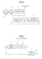
- a corresponding block diagram is shown in FIG. 5.
- the A / D converter 1 shown in FIG. 5 is operated with a free-running, ie non-regulated, sampling clock f T.
- the digital output signal of the A / D converter 1 is fed to the digital data receiver 2 via an interpolation unit 6.
- the interpolation unit 6 is in turn controlled by the output signal of the device 5, which calculates an ideal sampling phase as a function of the clock control criterion determined by the device 3 and feeds it to the interpolation unit 6, so that the interpolation unit 6 receives the data from the A / D converter 1 ( asynchronous) digital samples interpolated into corresponding synchronous samples.
- Both for the clock control variant shown in FIG is also for the clock control variant shown in FIG Determination of a suitable clock control criterion from a central one Importance.
- that generated by the device 3 Clock control criterion a measure of the phase error between the ideal sampling clock and the actual sampling clock be, the clock control criterion - if necessary after a suitable preprocessing - from the respective received signal is determined.
- non-decision feedback cycle control criteria are not the transmission symbol values estimated in the respective digital receiver (the so-called decision maker values) is used.
- decision maker values those estimated in the digital receiver Broadcast symbol values used.
- the present invention relates to the case of decision feedback Clock control.
- the adaptive equalizer 7 is used for equalizing the received signal, the coefficients of the adaptive equalizer 7 are variable.
- the decision maker 8 decides, i.e. determines the individual values of the received Transmission symbols.
- the device 3 depends in particular on the clock control criterion Trk from the input signal values of the adaptive equalizer 7 certainly.
- the clock control criterion determined with the arrangement shown in FIG. 6 Trk has a large spread because for the Generation of the clock control criterion Trk the distorted received signal is used. This in turn leads to one large phase jitter. If the clock control criterion Trk from the Output signal of the adaptive equalizer 7 are derived, the clock control criterion Trk would have less spread. However, this approach is problematic in that than that there is a coupling with the adaptive Equalizer 7 and thus set an unstable behavior would.
- a method for clock regulation of a digital receiver with the features of the preamble of claim 1 or a corresponding device according to the preamble of Claim 9 is known from WO 98/39873 A.
- the present invention is based on the object a method for clock control of a digital receiver and propose a corresponding device, whereby the problems described above can be solved and in particular a timing control criterion with minimal dispersion and additional stable control behavior can be obtained.
- the adaptive Equalizer for decoupling the adaptive Equalizer also generates a second part, the obtained from one or more equalizer coefficients and is combined with the first portion, in particular added. This is possible because the resulting coefficient values of the digital receiver equalizer from the sampling phase are dependent. In this way, on the one hand, it becomes a clock control criterion obtained with a minimal spread, that is leads to favorable jitter behavior. On the other hand by the decoupling from the adaptive equalizer described above ensures a stable control behavior.
- the second is sufficient Proportion of the clock control criterion, i.e. the decoupling or Correction variable, from only one or at most two coefficients of the adaptive equalizer.
- the Coefficient before the main coefficient and the coefficient after the main coefficient are particularly strong from the sampling phase dependent, so it only makes sense to use these two Coefficients or just one of these two coefficients for to use the generation of the decoupling size.
- the first part of the clock control criterion can be obtained in particular from the decision-maker error, ie from the difference between the input and output values of the decision-maker.
- k denotes the symbol or sampling time
- ⁇ y the Decision maker errors, i.e. the difference between the input and Initial value of the decision maker, and a that of the decision maker decided symbolic value.
- ⁇ y the Decision maker errors
- a the difference between the input and Initial value of the decision maker
- the invention described above can be general Clock control of any digital data receiver deploy.
- the invention is for both PAM (Pulse amplitude modulation) - as well as for CAP / QAM (carrierless Amplitude Modulation / Quadrature Amplitude Modulation) transmission systems applicable.
- the present invention relates essentially to the way in which the clock control criterion required for clock control is obtained. However, it is irrelevant to the invention how the clock control is actually carried out as a function of this clock control criterion.
- the present invention relates both to the variant of a direct control of the sampling clock f T shown in FIG. 4 and to the variant shown in FIG. 5 in which sampling is carried out with a free-running sampling clock f T and the asynchronous digital sampling values thus obtained are then interpolated become applicable.
- Fig. 1 is the basic structure of an inventive Device for determining a clock control criterion Trk shown.
- a first portion Trk1 of the clock control criterion of a device 10 from the signal immediately before the decision maker 8, i.e. after the adaptive equalizer 7, and the signal won after the decision maker 8. Since therefore for the determination the clock control criterion the signal after the adaptive Equalizer 7 is evaluated, a small spread of the Clock control criterion can be achieved. However, since without additional Measures with this procedure a coupling with the adaptive equalizer 7 and thus an unstable process occur would, the decoupling of the adaptive equalizer 7th from a device 9 a second portion Trk2 of the clock control criterion generated and from an adder 11 to the portion Trk1 added. The one thus obtained by the adder 11 Total value Trk Trk1 + Trk2 finally becomes the clock control on the basis and according to FIG. 4 and FIG. 5 the Loop filter 4 supplied.
- the second part Trk2 of the clock control criterion can thus be used as Correction or decoupling variable for the portion Trk1 that from the input signal and output signal of the decision maker 8 won is viewed.
- This decoupling variable Trk2 is evaluated by the device 9 by a Coefficients of the adaptive equalizer 7 obtained. This is possible because the coefficient values that arise in each case of the adaptive equalizer 7 depends on the sampling phase are. Through the decoupling brought about in this way from the adaptive equalizer 7 can a stable clock control behavior be achieved.
- the decoupling size Trk2 from only one or at most two coefficients of the adaptive equalizer 7 is obtained. Because the coefficient before the main coefficient and the coefficient after the main coefficient of the adaptive equalizer 7 in particular are heavily dependent on the sampling phase, it only makes sense these two coefficients or just one of these two coefficients to be used for the generation of the decoupling variable Trk2.
- the optimal sampling phase is here from the transmission channel, with a line-bound Transmission system, for example, depending on the line length.
- the optimal sampling phase there are optimal ones Equalizer coefficients.
- the generation of the decoupling size Trk2 through the device 9, which is used to develop the Clock control used by the adaptive equalizer 7 can now in such a way that the optimal equalizer coefficients set and thus the optimal sampling phase results.
- Trk2 K ⁇ (C -1 (K) -C -1 (Ref))
- the value k denotes the symbol or sampling time
- C -1 (k) denotes the equalizer coefficient before the main coefficient of adaptive equalizer 7
- C -1 (ref) denotes a predefinable reference value. In the steady state, the value of C -1 (k) will be set according to this reference value.
- the equalizer coefficient C -1 (k) considered in the optimal sampling phase, depending on the line length, is approximately in the range of 0.05 ... 0.3 based on the main coefficient.
- a suitable reference value C can then be obtained for each selected transmission line Generate -1 (ref).
- FIG. 2 A corresponding arrangement is shown in Fig. 2.
- a suitable reference value C -1 (ref) is generated with the aid of a device 12 depending on the digital AGC value of the digital reception arrangement.
- a subtractor 13 forms the difference between the equalizer coefficient C -1 (k) and the reference coefficient C -1 (ref).
- the output value of the multiplier 14 is finally fed to the adder 11 as a decoupling variable Trk2.
- Trk1 of the clock control criterion is calculated from the signal values before and after the decision maker 8.
- k denotes the symbol or sampling time
- ⁇ y the Decision maker errors, i.e. the difference from the input value of the decision maker 8 and the initial value of the decision maker 8, and a the decided initial value of the decision maker.
- ⁇ y (k) and a (k) can be used to generate the Portion Trk1 (k) also only the sign of ⁇ y (k) or a (k) can be used.
- Trk1 portion 3 is a corresponding arrangement for generation of the Trk1 portion.
- the difference between the input symbol value y (k) and the decided output symbol value a (k) of the decision maker 8 calculated, the output symbol value a (k) previously using a multiplier 15 multiplied by the decision-maker threshold 8 has been.
- the value is thus obtained from the subtractor 16 ⁇ y (k) output.
- a device 17 determines the sign this difference value.
- a delay element 19 gives accordingly the sign of the immediately preceding one Difference value ⁇ y (k-1).
- Another one Delay element 20 accordingly gives the sign of the immediately previous decided symbol value a (k-1) out.
- the method described above can also be used, for example, in a QAM or CAP transmission system.
- the demodulated received signal can be interpreted as a complex signal with real and imaginary parts.
- a complex-value adaptive equalizer 7 is required.
- the first part Trk1 of the clock control criterion can be generated both from the real part of the demodulated received signal and from the imaginary part of the demodulated received signal or from both parts (ie the sum of the clock control criteria determined from the real and imaginary parts).
- the same arrangement as in FIGS. 1-3 can be used for the decoupling.
- the coefficient C -1 (k) of the real part of the complex equalizer 7 is advantageously used here for decoupling.
Landscapes
- Engineering & Computer Science (AREA)
- Computer Networks & Wireless Communication (AREA)
- Signal Processing (AREA)
- Cable Transmission Systems, Equalization Of Radio And Reduction Of Echo (AREA)
- Dc Digital Transmission (AREA)
- Synchronisation In Digital Transmission Systems (AREA)
Claims (21)
- Procédé pour la régulation de cadence du récepteur numérique, le récepteur (2) numérique comprenant un correcteur de distorsion (7) adaptatif pour la correction de distorsion d'un signal de réception et un dispositif de décision (8) pour la détermination de valeurs de symbole du signal de réception, une première partie du critère de régulation de cadence (Trk1) étant obtenue par l'analyse du signal d'entrée et du signal de sortie du dispositif de décision (8),
une seconde partie du critère de régulation de cadence (Trk2) étant obtenue par l'analyse d'au moins un coefficient du correcteur de distorsion (7) adaptatif, et
le critère de régulation de cadence (Trk) étant obtenu par combinaison de la première partie du critère de régulation de cadence (Trk1) et de la seconde partie du critère de régulation de cadence (Trk2) et une cadence du récepteur (2) numérique étant régulée en fonction du critère de régulation de cadence,
caractérisé en ce que
la seconde partie du critère de régulation de cadence (Trk2) pour la dissociation de la régulation de cadence du correcteur de distorsion adaptatif est obtenue par la soustraction entre au moins un coefficient analysé du correcteur de distorsion (7) adaptatif et une valeur de référence prédéfinie. - Procédé selon la revendication 1,
caractérisé en ce que le critère de régulation de cadence (Trk) est obtenu par l'addition de la première partie du critère de régulation de cadence (Trk1) et de la seconde partie du critère de régulation de cadence (Trk2). - Procédé selon la revendication 1 ou la revendication 2,
caractérisé en ce que
la première partie du critère de régulation de cadence (Trk1) est obtenue par une soustraction entre le signal d'entrée et le signal de sortie du dispositif de décision (8). - Procédé selon l'une quelconque des revendications précédentes,
caractérisé en ce que
les valeurs individuelles de la première partie du critère de régulation de cadence sont déterminées par la relation :
k désignant le moment, Trk1(k) les valeurs de la première partie du critère de régulation de cadence, y(k) les valeurs d'entrée du dispositif de décision (8) et a(k) les valeurs de sortie du dispositif de décision (8). - Procédé selon l'une quelconque des revendications précédentes,
caractérisé en ce que
la seconde partie du critère de régulation de cadence (Trk2) est obtenue par l'analyse de au plus deux coefficients du correcteur de distorsion (7) adaptatif. - Procédé selon la revendication 5,
caractérisé en ce que
la seconde partie du critère de régulation de cadence (Trk2) est obtenue par l'analyse du coefficient (C-1) avant le coefficient principal et/ou du coefficient après le coefficient principal du correcteur de distorsion (7) adaptatif. - Procédé selon la revendication 6,
caractérisé en ce que
les valeurs individuelles de la seconde partie du critère de régulation de cadence sont obtenues selon la relation suivante : - Procédé selon la revendication 7,
caractérisé en ce que
on applique la relation K = 2L pour le facteur de cadrage réel, L étant un nombre entier. - Dispositif pour la régulation de cadence d'un récepteur numérique, le récepteur (2) numérique comprenant un correcteur de distorsion (7) adaptatif pour la correction de distorsion d'un signal de réception et un dispositif de décision (8) pour la détermination de valeurs de symbole du signal de réception, avec un appareil (3) pour l'obtention d'un critère de régulation de cadence (Trk) à partir du signal de réception,
l'appareil (3) comprenant des premiers moyens (10) pour l'obtention d'une première partie du critère de régulation de cadence (Trk1) par l'analyse du signal d'entrée et du signal de sortie du dispositif de décision (8), des seconds moyens (9) pour l'obtention d'une seconde partie du critère de régulation de cadence (Trk2) par l'analyse au moins d'un coefficient du correcteur de distorsion (7) adaptatif et
des moyens de combinaison (11) pour l'obtention du critère de régulation de cadence (Trk) par la combinaison de la première partie du critère de régulation de cadence (Trk1) avec la seconde partie du critère de régulation de cadence (Trk2) et
avec un circuit régulateur de cadence (3-6) pour la génération d'une cadence, régulée en fonction du critère de régulation de cadence (Tkr), du récepteur (2) numérique,
caractérisé en ce que
les seconds moyens (9) sont conçus de telle sorte que, pour la dissociation de la régulation de cadence du correcteur de distorsion (7) adaptatif, ils déterminent la seconde partie de la régulation de cadence (Trk2) par la soustraction entre le moins un coefficient (C-1) analysé du correcteur de distorsion (7) adaptatif et une valeur de référence (C-1(ref)) prédéfinie. - Dispositif selon la revendication 9,
caractérisé en ce que
les moyens de combinaison (11) sont conçus sous la forme d'un additionneur. - Dispositif selon la revendication 9 ou la revendication 10,
caractérisé en ce que
les premiers moyens (10) pour le calcul des valeurs individuelles de la première partie du critère de régulation de cadence sont conçus selon l'une des relations suivantes :
k désigne le moment, Trk1(k) les valeurs individuelles de la première partie du critère de régulation de cadence, y(k) les valeurs d'entrée du dispositif de décision (8) et a(k) les valeurs de sortie du dispositif de décision (8). - Dispositif selon l'une quelconque des revendications 9 à 11,
caractérisé en ce que
les seconds moyens (9) pour l'obtention de la seconde partie du critère de régulation de cadence (Trk2) sont conçus par l'analyse d'au maximum deux coefficients du correcteur de distorsion (8) adaptatif. - Dispositif selon la revendication 12,
caractérisé en ce que
les seconds moyens (9) pour l'obtention de la seconde partie du critère de régulation de cadence (Trk2) sont conçus par l'analyse du coefficient (C-1) avant le coefficient principal du correcteur de distorsion (7) adaptatif et/ou du coefficient après le coefficient principal du correcteur de distorsion (7) adaptatif. - Dispositif selon la revendication 13,
caractérisé en ce que
les seconds moyens (9) sont conçus pour le calcul des valeurs individuelles de la seconde partie du critère de régulation de cadence selon la relation suivante : - Dispositif selon la revendication 14,
caractérisé en ce que
on a la relation K = 2L pour le facteur de cadrage réel, L étant un nombre entier. - Dispositif selon l'une quelconque des revendications 9 à 15,
caractérisé en ce que
le dispositif de décision (8) est monté en aval du correcteur de distorsion (7) adaptatif. - Utilisation d'un dispositif selon l'une quelconque des revendications 9 à 16 pour la régulation de la cadence de balayage d'un récepteur (2) numérique dans un système de transmission PAM.
- Utilisation d'un dispositif selon l'une quelconque des revendications 9 à 16 pour la régulation de la cadence de balayage d'un récepteur (2) numérique dans un système de transmission, le signal de réception étant présent sous la forme d'un signal complexe avec une partie réelle et une partie imaginaire,
le correcteur de distorsion (7) adaptatif du récepteur (2) numérique étant une valeur complexe. - Utilisation selon la revendication 18,
caractérisée en ce que
la première partie du critère de régulation de cadence (Trk1) est obtenue à partir de la partie réelle et/ou de la partie imaginaire du signal de réception. - Utilisation selon la revendication 18 ou la revendication 19,
caractérisée en ce que
la seconde partie du critère de régulation de cadence (Trk2) est obtenue par l'analyse d'au moins un coefficient de la partie réelle du correcteur de distorsion (7) adaptatif à valeur complexe. - Utilisation selon l'une quelconque des revendications 18 à 20,
caractérisée en ce que
le système de transmission est un système de transmission QAM ou CAP.
Applications Claiming Priority (3)
| Application Number | Priority Date | Filing Date | Title |
|---|---|---|---|
| DE10025566A DE10025566C2 (de) | 2000-05-24 | 2000-05-24 | Verfahren und Vorrichtung zur Taktregelung eines digitalen Empfängers |
| DE10025566 | 2000-05-24 | ||
| PCT/EP2001/005518 WO2001091361A1 (fr) | 2000-05-24 | 2001-05-15 | Procede et dispositif de regulation de cadence d'un recepteur numerique |
Publications (2)
| Publication Number | Publication Date |
|---|---|
| EP1284064A1 EP1284064A1 (fr) | 2003-02-19 |
| EP1284064B1 true EP1284064B1 (fr) | 2004-12-22 |
Family
ID=7643293
Family Applications (1)
| Application Number | Title | Priority Date | Filing Date |
|---|---|---|---|
| EP01943370A Expired - Lifetime EP1284064B1 (fr) | 2000-05-24 | 2001-05-15 | Procede et dispositif de regulation de cadence d'un recepteur numerique |
Country Status (6)
| Country | Link |
|---|---|
| US (1) | US20030152180A1 (fr) |
| EP (1) | EP1284064B1 (fr) |
| JP (1) | JP3644928B2 (fr) |
| CN (1) | CN1262086C (fr) |
| DE (2) | DE10025566C2 (fr) |
| WO (1) | WO2001091361A1 (fr) |
Families Citing this family (13)
| Publication number | Priority date | Publication date | Assignee | Title |
|---|---|---|---|---|
| DE10204190C1 (de) | 2002-02-01 | 2003-06-18 | Infineon Technologies Ag | Taktregelungsschaltung zur Taktphasenregelung eines Transceivers |
| DE10212913C1 (de) * | 2002-03-22 | 2003-10-23 | Infineon Technologies Ag | Berechnungsschaltung zur Berechnung eines Taktregelkriteriums |
| US7274762B2 (en) * | 2002-03-22 | 2007-09-25 | Infineon Technologies Ag | Calculation circuit for calculating a sampling phase error |
| US7480326B2 (en) * | 2002-07-17 | 2009-01-20 | Broadcom Corporation | Channel diagnostic systems and methods |
| US7239680B2 (en) * | 2002-07-17 | 2007-07-03 | Broadcom Corporation | Methods for performing channel diagnostics |
| US7200194B2 (en) * | 2002-10-11 | 2007-04-03 | Spreadtrum Communications Corporation | Receiver signal dynamic range compensation based on received signal strength indicator |
| US6977600B2 (en) * | 2004-02-20 | 2005-12-20 | Fujitsu Limited | Determining analog error using parallel path sampling |
| US7489749B2 (en) * | 2004-02-24 | 2009-02-10 | Ming-Kang Liu | Optimum phase timing recovery in the presence of strong intersymbol interference |
| DE102004047702B4 (de) * | 2004-09-30 | 2015-02-05 | Lantiq Deutschland Gmbh | Verfahren und Vorrichtung zur Bestimmung eines Schätzfehlers eines Entscheiders sowie Entzerrer |
| DE102005008989B4 (de) * | 2005-02-28 | 2007-06-28 | Infineon Technologies Ag | Verfahren und Vorrichtung zur Bestimmung einer Ausgangsfolge aus einer Eingangsfolge |
| WO2007109740A2 (fr) * | 2006-03-21 | 2007-09-27 | Serious Usa, Inc. | Cartes de données optiques et transactions |
| US7916780B2 (en) * | 2007-04-09 | 2011-03-29 | Synerchip Co. Ltd | Adaptive equalizer for use with clock and data recovery circuit of serial communication link |
| EP2086158B1 (fr) * | 2008-01-29 | 2011-06-22 | Alcatel Lucent | Schéma de récupération d'horloge pour un récepteur optique basé sur la surveillance du précurseur et postcurseur des coefficients de prise |
Family Cites Families (5)
| Publication number | Priority date | Publication date | Assignee | Title |
|---|---|---|---|---|
| US3697689A (en) * | 1970-12-23 | 1972-10-10 | North American Rockwell | Fine timing recovery system |
| JPH09294095A (ja) * | 1996-04-26 | 1997-11-11 | Oki Electric Ind Co Ltd | 適応等化器 |
| US6249557B1 (en) * | 1997-03-04 | 2001-06-19 | Level One Communications, Inc. | Apparatus and method for performing timing recovery |
| TW329493B (en) * | 1997-06-18 | 1998-04-11 | Winbond Electronics Corp | Data processing device |
| US6249395B1 (en) * | 1998-12-08 | 2001-06-19 | Stmicroelectronics, N.V. | Data recovery system particularly for systems utilizing partial response maximum likelihood detection |
-
2000
- 2000-05-24 DE DE10025566A patent/DE10025566C2/de not_active Expired - Fee Related
-
2001
- 2001-05-15 EP EP01943370A patent/EP1284064B1/fr not_active Expired - Lifetime
- 2001-05-15 WO PCT/EP2001/005518 patent/WO2001091361A1/fr not_active Ceased
- 2001-05-15 CN CNB018100155A patent/CN1262086C/zh not_active Expired - Fee Related
- 2001-05-15 US US10/296,118 patent/US20030152180A1/en not_active Abandoned
- 2001-05-15 DE DE50104889T patent/DE50104889D1/de not_active Expired - Fee Related
- 2001-05-15 JP JP2001586831A patent/JP3644928B2/ja not_active Expired - Fee Related
Also Published As
| Publication number | Publication date |
|---|---|
| WO2001091361A1 (fr) | 2001-11-29 |
| US20030152180A1 (en) | 2003-08-14 |
| EP1284064A1 (fr) | 2003-02-19 |
| DE10025566C2 (de) | 2003-04-30 |
| JP2003534713A (ja) | 2003-11-18 |
| CN1262086C (zh) | 2006-06-28 |
| DE10025566A1 (de) | 2001-12-06 |
| JP3644928B2 (ja) | 2005-05-11 |
| DE50104889D1 (de) | 2005-01-27 |
| CN1443408A (zh) | 2003-09-17 |
Similar Documents
| Publication | Publication Date | Title |
|---|---|---|
| EP1284064B1 (fr) | Procede et dispositif de regulation de cadence d'un recepteur numerique | |
| DE19680412B4 (de) | Symbolzeitpunkt-Rückgewinnungsschaltung und zugehöriges Verfahren | |
| DE69421834T2 (de) | Digitale Taktrückgewinnungsschaltung | |
| DE60027553T2 (de) | Auslöschbasierte sofortige Regelkreissteuerung in einem Datenempfänger | |
| DE2729312C2 (de) | Verfahren und Schaltungsanordnungen zur Synchronisierung von Taktsignalen | |
| WO2004028046A1 (fr) | Procede de transmission de signaux multiplex de polarisation optique | |
| DE10133898C1 (de) | Empfänger mit einem integrierten Taktphasendetektor | |
| EP0412616A2 (fr) | Récepteur pour signaux de données distordus de faÀ§on temporellement variable | |
| DE69826439T2 (de) | Verfahren und vorrichtung zur ausführung von taktrückgewinnung | |
| DE69737220T2 (de) | Synchronisationsgerät | |
| DE10112773B4 (de) | Verfahren zur Frequenz- und Zeit-Synchronisation eines OFDM-Empfängers | |
| DE102008026391A1 (de) | Verfahren und Vorrichtung zur Synchronisation eines Taktsignals mit einem Referenztaktsignal | |
| EP3876491A1 (fr) | Émetteur et récepteur et procédés correspondants | |
| DE19755897B4 (de) | Vorrichtung zur Synchronisierung eines Nachrichtenempfängers | |
| EP0829990B1 (fr) | Procédé de démodulation de signaux M-QAM à haut niveau sans connaissance de données transmises | |
| WO2003019889A2 (fr) | Procede de reconstitution de donnees transmises par l'intermediaire d'une ligne de transmission dans un recepteur et dispositif correspondant | |
| DE69317392T2 (de) | Abtastfrequenzumwandler | |
| DE102006031331B3 (de) | Digitaler Phasendetektor und Verfahren zur Erzeugung eines digitalen Phasendetektionssignals | |
| DE10354558B4 (de) | Vorrichtung zum Erzeugen eines Sendetaktsignals und eines Empfangstaktsignals für eine Sende- und Empfangsvorrichtung | |
| DE69824898T2 (de) | Schätzung der kanalimpulsantwort mittels der streuung vom empfangenen signal | |
| DE60317276T2 (de) | Synchronisierung in Mehrträgerempfängern | |
| WO1999009695A2 (fr) | Procede pour supprimer les parasites dans un courant de donnees bipolaire et circuiterie pour mettre ledit procede en oeuvre | |
| DE10204190C1 (de) | Taktregelungsschaltung zur Taktphasenregelung eines Transceivers | |
| DE10212913C1 (de) | Berechnungsschaltung zur Berechnung eines Taktregelkriteriums | |
| DE10010947A1 (de) | Takt- und Datenregenerator für unterschiedliche Datenraten |
Legal Events
| Date | Code | Title | Description |
|---|---|---|---|
| PUAI | Public reference made under article 153(3) epc to a published international application that has entered the european phase |
Free format text: ORIGINAL CODE: 0009012 |
|
| 17P | Request for examination filed |
Effective date: 20021024 |
|
| AK | Designated contracting states |
Designated state(s): AT BE CH CY DE DK ES FI FR GB GR IE IT LI LU MC NL PT SE TR |
|
| 17Q | First examination report despatched |
Effective date: 20031112 |
|
| GRAP | Despatch of communication of intention to grant a patent |
Free format text: ORIGINAL CODE: EPIDOSNIGR1 |
|
| RBV | Designated contracting states (corrected) |
Designated state(s): DE FR GB |
|
| GRAS | Grant fee paid |
Free format text: ORIGINAL CODE: EPIDOSNIGR3 |
|
| GRAA | (expected) grant |
Free format text: ORIGINAL CODE: 0009210 |
|
| AK | Designated contracting states |
Kind code of ref document: B1 Designated state(s): DE FR GB |
|
| REG | Reference to a national code |
Ref country code: GB Ref legal event code: FG4D Free format text: NOT ENGLISH |
|
| REG | Reference to a national code |
Ref country code: IE Ref legal event code: FG4D Free format text: GERMAN |
|
| REF | Corresponds to: |
Ref document number: 50104889 Country of ref document: DE Date of ref document: 20050127 Kind code of ref document: P |
|
| GBT | Gb: translation of ep patent filed (gb section 77(6)(a)/1977) |
Effective date: 20050314 |
|
| PLBE | No opposition filed within time limit |
Free format text: ORIGINAL CODE: 0009261 |
|
| STAA | Information on the status of an ep patent application or granted ep patent |
Free format text: STATUS: NO OPPOSITION FILED WITHIN TIME LIMIT |
|
| ET | Fr: translation filed | ||
| 26N | No opposition filed |
Effective date: 20050923 |
|
| PGFP | Annual fee paid to national office [announced via postgrant information from national office to epo] |
Ref country code: FR Payment date: 20060519 Year of fee payment: 6 |
|
| PGFP | Annual fee paid to national office [announced via postgrant information from national office to epo] |
Ref country code: GB Payment date: 20060522 Year of fee payment: 6 |
|
| PGFP | Annual fee paid to national office [announced via postgrant information from national office to epo] |
Ref country code: DE Payment date: 20060717 Year of fee payment: 6 |
|
| GBPC | Gb: european patent ceased through non-payment of renewal fee |
Effective date: 20070515 |
|
| REG | Reference to a national code |
Ref country code: FR Ref legal event code: ST Effective date: 20080131 |
|
| PG25 | Lapsed in a contracting state [announced via postgrant information from national office to epo] |
Ref country code: DE Free format text: LAPSE BECAUSE OF NON-PAYMENT OF DUE FEES Effective date: 20071201 |
|
| PG25 | Lapsed in a contracting state [announced via postgrant information from national office to epo] |
Ref country code: GB Free format text: LAPSE BECAUSE OF NON-PAYMENT OF DUE FEES Effective date: 20070515 |
|
| PG25 | Lapsed in a contracting state [announced via postgrant information from national office to epo] |
Ref country code: FR Free format text: LAPSE BECAUSE OF NON-PAYMENT OF DUE FEES Effective date: 20070531 |