EP2086158B1 - Schéma de récupération d'horloge pour un récepteur optique basé sur la surveillance du précurseur et postcurseur des coefficients de prise - Google Patents
Schéma de récupération d'horloge pour un récepteur optique basé sur la surveillance du précurseur et postcurseur des coefficients de prise Download PDFInfo
- Publication number
- EP2086158B1 EP2086158B1 EP08290079A EP08290079A EP2086158B1 EP 2086158 B1 EP2086158 B1 EP 2086158B1 EP 08290079 A EP08290079 A EP 08290079A EP 08290079 A EP08290079 A EP 08290079A EP 2086158 B1 EP2086158 B1 EP 2086158B1
- Authority
- EP
- European Patent Office
- Prior art keywords
- tap coefficients
- signal
- clock
- precursor
- delay lines
- Prior art date
- Legal status (The legal status is an assumption and is not a legal conclusion. Google has not performed a legal analysis and makes no representation as to the accuracy of the status listed.)
- Active
Links
Images



Classifications
-
- H—ELECTRICITY
- H04—ELECTRIC COMMUNICATION TECHNIQUE
- H04L—TRANSMISSION OF DIGITAL INFORMATION, e.g. TELEGRAPHIC COMMUNICATION
- H04L7/00—Arrangements for synchronising receiver with transmitter
- H04L7/0054—Detection of the synchronisation error by features other than the received signal transition
- H04L7/0058—Detection of the synchronisation error by features other than the received signal transition detection of error based on equalizer tap values
Definitions
- the invention relates to optical communication systems, in particular to an apparatus and a method for clock recovery for use in a fiber optics receiver.
- a clock recovery circuit uses a phase locked loop (PLL).
- PLL phase locked loop
- an analog phase comparator within the clock recovery circuit compares phase information of the received data signal (in particular the phase information of data transitions), with the phase of a locally generated clock signal, thereby generating a phase error signal characterizing the phase difference.
- the phase error signal is typically low pass filtered (i.e., integrated) before being fed to the input of a voltage controlled oscillator (VCO), with the VCO generating the local clock signal.
- VCO voltage controlled oscillator
- the output frequency of the VCO depends on the input voltage of the VCO.
- the photodetector at the receiver is typically directly fed by on-off modulated light and the resulting current of the photodetector corresponds to the received optical power.
- the phase information is lost (however, with differential detection, phase difference between adjacent bits can be recovered).
- coherent detection receivers the received optical light is coherently superpositioned with a single-frequency optical local oscillator (LO) signal.
- LO optical local oscillator
- Such coherent detection receivers allow detecting the phase of the received signal as necessary for phase modulation schemes (e.g., QPSK - quadrature phase shift keying).
- phase modulation schemes e.g., QPSK - quadrature phase shift keying.
- homodyne detection the carrier frequency of the received optical signal and the frequency of the LO signal coincide.
- digital clock recovery schemes may be used which are more tolerant to optical distortion.
- one may use oversampling processing after digital CD compensation.
- existing digital clock recovery schemes in particular digital clock recovery schemes based on oversampling of the received signal, require high processing power and thus suffer from high power dissipation.
- US 4,334,313 discloses a timing recovery scheme.
- the receiver timing is adjusted such that two coefficients in a queue of equalizer coefficients, one on either side of the boundary between the front and back portions of the queue, are maintained substantially equal in complex magnitude.
- the location of the coefficient having the largest complex magnitude is identified in each symbol interval. If this coefficient is found to be in the front of the queue, a retard signal is generated. Otherwise, i.e., if this coefficient is found in the back of the queue, an advance signal is generated.
- a first aspect of the invention relates to a clock recovery apparatus for use in an optical receiver, in particular for use in a coherent receiver.
- Such receiver comprises electrical sampling means clocked by a clock signal for sampling a received signal, in particular one or more ADCs (analog-digital-converter).
- ADCs analog-digital-converter
- the sampling means may be also realized in form of fully-digital re-sampling means.
- the coefficients determining means may be configured to carry out a constant modulus algorithm (CMA) for determining the tap coefficients.
- CMA constant modulus algorithm
- other algorithms may be used for determining the tap coefficients.
- the inventive clock recovery apparatus is based on using information of tap coefficients and controlling the frequency of a local generated clock in dependency of the information of the tap coefficients.
- precursor and postcursor tap coefficients are more or less balanced. However, if the clock is not locked, the coefficients become unbalanced. Such imbalance may be determined by the comparison means and the information is used for controlling the frequency of the clock signal, which is generated in clock generation means.
- the filter and the delay lines may be realized in digital hardware (e.g., an ASIC - application-specific integrated circuit; or an FPGA - field-programmable gate array) or in software by using a DSP (digital signal processor).
- digital hardware e.g., an ASIC - application-specific integrated circuit; or an FPGA - field-programmable gate array
- DSP digital signal processor
- a second aspect of the invention relates to an optical receiver, in particular to a coherent receiver, comprising a clock recovery apparatus as discussed above.
- the above remarks related to the clock recovery apparatus and its preferred embodiments are basically also applicable to the receiver according to the second aspect of the invention.
- the receiver comprises an adaptive multi-tap filter comprising four tapped delay lines being part of a polarization demultiplexer or being downstream of a polarization demultiplexer and precursor and postcursor tap coefficients associated to the four delay lines are compared to control the frequency of the clock signal. This is performed by comparing a weight of precursor tap coefficients associated to the four tapped delay lines and a weight of postcursor tap coefficientts associated to the four tapped delay lines.
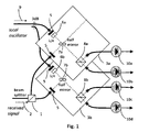
- Fig. 1 shows an embodiment of the optical part of a phase-diversity and polarization-diversity coherent receiver with polarization multiplexing functionality.
- the coherent receiver is configured for receiving and demultiplexing a polarization division multiplexed (PDM) optical signal.
- PDM polarization division multiplexed
- Polarization division multiplexed formats are often used in combination with coherent detection.
- the transmitted PDM signal comprises a first signal component (e.g., a first QPSK signal) having a first polarization and a second signal component (e.g., a second QPSK signal) having a second polarization orthogonal to the first polarization.
- the receiver in Fig. 1 is configured to generate in-phase and quadrature-phase components (phase-diversity) of the downconverted received signal for two orthogonal polarizations (polarization-diversity).
- the receiver comprises a polarization beam splitter (PBS) 1, which splits the received optical signal 2 into a first optical wave and a second optical wave, with the polarizations of the first and second optical waves being orthogonal. Due to shifting of the polarization along the fiber, the signals of the first and second optical waves typically do not correspond to the first and second components of the transmitted PDM signal, respectively.
- PBS polarization beam splitter
- the first optical wave is fed to a first coherent demodulator 3a
- the second optical wave is fed to a second coherent demodulator 3b.
- Both the first coherent demodulator 3a and the second coherent demodulator 3b receive a local oscillator (LO) signal 9 for superimposing the first optical wave and the second optical wave with the LO signal 9, respectively.
- LO local oscillator
- the carrier frequency of the received optical signal 2 and the frequency of the LO signal 9 coincide.
- Polarizers 5 at the inputs of the demodulators 3a and 3b can be used to improve the polarization quality.
- polarizers 5 at the LO input of both demodulators 3a, 3b a ⁇ /4 wave plate 6a, 6b is provided.
- the wave plates 6a, 6b are used for making the polarization of the LO signal 9 circular, while the signal remains linearly polarized.
- PBS 8a, 8b After passing through half mirrors 7a, 7b for superimposing the LO signal 9 and received signals, PBS 8a, 8b are used for each generating two orthogonal phases.
- the polarization angle of the signal when hitting half mirrors 7a, 7b is 45° with respect to the principal axis of PBS 8a, 8b.
- the four outputs of the two demodulators 3a, 3b are coupled to the inputs of four photodiodes 10a-10d, thereby generating four electrical currents I 10a , I 10b , I 10c , I 10d .
- the beat term of current I 10a of photodiode 10a corresponds to the quadrature-phase component of a first polarization of the downconverted signal.
- the first polarization corresponds to the polarization of the first wave as generated by PBS 1.
- the beat term of current I 10b of photodiode 10b corresponds to the in-phase component of the first polarization of the downconverted signal.
- the beat term of current I 10c of photodiode 10c corresponds to the quadrature-phase component of a second polarization of the downconverted signal.
- the second polarization corresponds to the polarization of the second wave as generated by PBS 1.
- the beat term of current I 10d of photodiode 10d corresponds to the in-phase component of the second polarization of the downconverted signal.
- the downconverted signal components for both polarizations are fed to four ADCs 11a-11d for sampling the signal components.
- the ADCs 11 a-11d are clocked by a clock signal supplied by a clock block 12.
- the clock block 12 is configured to supply and (optionally convert) a clock signal as generated by a VCO 13 to the ADCs 11a-11d.
- the clock block 12 may comprise, e.g., one or more clock tree amplifiers, frequency converters (e.g., frequency dividers or multipliers) and/or phase shifters.
- the received digital signals are processed in a digital signal processor (DSP) or in customized digital hardware (or in a combination of both).
- DSP digital signal processor
- the digital output signal of ADC 11a (corresponding to the quadrature-phase component) is multiplied by "j" and added to the digital output signal of ADC 11b (corresponding to the in-phase component).
- the two resulting complex signals are fed in two CD compensation blocks 14a, 14b for compensating CD in the digital domain.
- the two complex output signals x 1 , x 2 of the CD compensation blocks 14a, 14b are fed to a polarization demultiplexing unit and equalization unit 15.
- clock recovery can only be done after compensation of CD (within the DSP). Thus, no standard clock recovery method can be used.
- off-line processing was used having a digital clock recovery block inserted between CD compensation blocks 14a, 14b and polarization demultiplexing and equalization unit 15.
- this approach is only feasible for off-line processing because it involves over-sampling routines that are extremely power-consuming and hence inappropriate for real-time implementation.
- the results from a multi-tap filter used for demultiplexing and/or equalization are used to tune the output frequency of the clock block 12 that clocks the ADCs 11a-11d by the help of a feedback through the VCO 13.
- a feedback signal for clock recovery is extracted from adaptive filter coefficients in the polarization demultiplexer and equalization unit 15.
- the polarization demultiplexing and equalization unit 15 is used to rotate the received signal components x 1 , x 2 for recovering the initial polarization components as multiplexed in the transmitter and for removing interferences between the two polarization components.
- the elements h ij of the rotation matrix represent the coefficients of an adaptive filter, which are temporally updated.
- the coefficients h ij are complex numbers.
- the precursor samples are the samples x 1,2 (k) to x 1,2 (k-N/2+1)
- the postcursor samples are the samples x 1,2 (k-N/2-1) to x 1,2 (k-N).
- the filter as described by the above equation processes at the same time a plurality of samples which are temporally spaced or delayed by one symbol length (T-spaced) or half a symbol length (T/2-spaced).
- the samples used for the filter are called “taps” and the expression "(N+1)-taps filter” means that the filter uses N neighboring taps around a central tap.
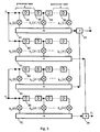
- Fig. 3 illustrates an embodiment for such an (N+1)-taps adaptive filter corresponding to the above equation which may be used in the polarization demultiplexing and equalization unit 15.
- the filter and the delay lines may be implemented in digital hardware or in software by using a DSP.
- the filter comprises four FIR sub-filters (finite impulse response).
- Each FIR sub-filter comprises four tapped delay lines, each tapped delay line comprising N identical delay elements 30 having a delay of one symbol length or alternatively a delay of a fraction of a symbol length, e.g., half the symbol length.
- Each delay line has precursor taps and postcursor taps located around the main tap, with the main tap being the central tap.
- Each tap of the N+1 taps of each delay line is multiplied by a coefficient h ij .
- the multiplied tap values of each tapped delay line are summed in adders 31.
- the first complex signal x 1 associated to a first polarization is fed to the first and second delay lines (numbering of delay lines from top to bottom in Fig. 3 ), whereas the second complex signal x 2 associated to a second polarization is fed to the third and fourth delay lines.
- the outputs of the adders 31 associated to the first and third delay lines are combined by an adder 33, with the output signal y 2 of adder 33 corresponding to the first multiplexed polarization component.
- the outputs of the adders 31 associated to the second and fourth delay lines are combined by an adder 34, with the output signal y 2 of adder 34 corresponding to the second multiplexed polarization component.
- the two adders 31 associated to the first and third delay lines and adder 33 may be combined.
- the two adders 31 associated to second and fourth delay lines and adder 34 may be combined.
- the magnitude of the tap coefficients h ij is decreasing from the main tap (here the central tap) towards the neighboring taps and the main tap should have the highest value.
- the tap coefficients h ij have large values for the central taps and very low values on the neighboring taps.
- said property of the tap coefficients in the polarization demultiplexing and equalization unit 15 is used to tune the frequency of the clock signal driving the ADCs 11a-11d by means of a feedback (see feedback in Fig. 2 from the polarization demultiplexing block 15 via the VCO control block 16, via the VCO 13, via the clock block 12 to the ADCs 11a-11d).
- the precursor coefficients h ij (0) to h ij (N/2-1) and the postcursor coefficients h ij (N/2+1) to h ij (N) are balanced around the central tap coefficients h ij (N/2).
- the weights of these coefficients become unbalanced.
- the frequency of the recovered clock has to be increased and vice versa.
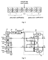
- Fig. 5 illustrates a first embodiment of the polarization demultiplexing and equalization unit 15 in Fig. 2 and an embodiment of the feedback loop for clock recovery.
- the polarization multiplexing and equalization unit 15 comprises four FIR sub-filters for polarization demultiplexing and signal equalization. In Fig. 5 only the tap coefficients of the FIR sub-filters are shown.
- a constant modulus algorithm (CMA) is used, i.e., the tap coefficients h ij of the filter are computed by means of the CMA.
- CMA blocks 40, 41 are provided for performing the CMA and computing the tap coefficients h ij .
- the CMA blocks update the tap coefficients h ij in dependency on the current output values y 1 , y 2 of the polarization multiplexer.
- 2 and ⁇ y 2 1-
- the terms h ij ' denote the updated vectors of tap coefficients h ij (0) to h ij (N)
- the terms h ij denote the actual vectors of tap coefficients h ij (0) to h ij (N)
- ⁇ is a convergence parameter
- the terms x j * denote the actual vector of the complex conjugate of the samples x j (k) to x j (k - N).
- the updated tap coefficients h ij are computed in dependency of the samples x j (k) to x j (k - N) as apparent from the above equations.
- the VCO control block 16 receives the tap coefficients h ij and determines the weight w post of the postcursor coefficients and the weight w pre of the precursor coefficients. If the weight w pre of the precursor coefficients is larger than the weight w post of the postcursor coefficients, a feedback signal is sent to the VCO input to increase the frequency of the recovered clock signal. If the weight w pre of the precursor coefficients is smaller than the weight w post of the postcursor coefficients, a feedback signal is sent to the VCO input to decrease the frequency of the recovered clock signal.
- the VCO control block 16 may also comprise a loop filter, e.g., a low-pass filter. Instead of the VCO control block 16, the CMA blocks may calculate the weights w post and w pre and optionally generate also a comparison signal.
- Fig. 6 shows exemplary time dependent courses of the weight w post of the postcursor coefficients and the weight w precursor of the precursor coefficients computed from an experimental data file.
- the illustrated weights w post and w pre are given in an arbitrary unit.
- a 5-taps T/2-spaced filter is used (in total 4 ⁇ 5 taps).
- the frequency of the clock signal here: 10.709228 GHz
- Fig. 6 shows that the weights w post and w pre are almost perfectly balanced.
- the bit error ratio (BER) is measured to 1 ⁇ 10 -4 .
- Fig. 7 shows the time dependent courses of the weights w post and w pre when the clock was intentionally shifted by an amount of 100 KHz leading to a clock frequency of 10.709128 GHz (the feedback loop in Fig. 5 is not closed).
- the weights w post and w pre are diverging and most of all not balanced anymore. Due to the frequency shift, the measured BER increases to 2.6 ⁇ 10 -2 .
- the weight w post of the postcursor coefficients is larger than the weight w pre of the precursor coefficients indicating that the frequency of the clock signal has to be increased.
- a feedback signal has to be sent to the clock generation means, i.e., to the VCO 13 to increase the clock frequency.
- Fig. 8 shows the time dependent courses of the weights w prost and w pre when the feedback loop is closed and the results from the polarization demultiplexing are fed back.
- the starting clock frequency is set to 10.709128 GHz (i.e., initially the clock frequency has an offset of 100 KHz). Due to the feedback, the frequency of the clock signal is corrected and the clock signal locks to the incoming data signal, thereby the weight w post and w pre tend to converge to the same values resulting to a measured BER of 1.4 ⁇ 10 -4
- Fig. 9 illustrates a second embodiment of the polarization demultiplexing and equalization unit 15 in Fig. 2 .
- the unit 15 in Fig. 9 is composed of two parts, a single tap polarization demultiplexer 15a and a multi-tap equalizer 15b.
- Using a separate polarization demultiplexer 15a as shown in Fig. 9 may improve the convergence behavior.
- the polarization demultiplexer 15a performs the rotation function as explained above. In practice, polarization demultiplexing may be not done perfectly by the polarization demultiplexer 15a.
- the equalizer 15b comprises four delay lines associated to four equalizer sub-filters.
- the structure of the equalizer 15b corresponds to the structure of the multi-tap filter in Fig. 3 .
- the tap coefficients of the demultiplexer 15a are determined by using the CMA as explained above (in Fig. 9 the CMA units for computing the coefficients are not shown). Also, the tap coefficients h ij of the equalizer 15b are determined by using the CMA as explained above.
- the equalizer 15b may be connected upstream of the demultiplexer 15a. Further, in both cases the equalizer 15b may have only two delay lines (one delay line per signal path) instead of four delay lines.
Landscapes
- Engineering & Computer Science (AREA)
- Computer Networks & Wireless Communication (AREA)
- Signal Processing (AREA)
- Optical Communication System (AREA)
- Synchronisation In Digital Transmission Systems (AREA)
Claims (10)
- Appareil de récupération d'horloge destiné à être utilisé dans un récepteur optique, le récepteur comprenant :- des moyens électriques (11a-d) synchronisés par un signal d'horloge pour échantillonner un signal reçu ; et- un filtre adaptatif à prises multiples (30, 31, 33, 34) comprenant quatre lignes à retard à prises faisant partie d'un démultiplexeur à polarisation ou se trouvant en aval d'un démultiplexeur à polarisation, le filtre étant connecté en aval des moyens électriques et recevant des coefficients de prise ajustables ;l'appareil de récupération d'horloge étant caractérisé par- des moyens de comparaison (16) pour comparer les coefficients de prise pré-curseur et post-curseur associés aux quatre lignes à retard à prises, les moyens de comparaison (16) étant configurés pour comparer- un poids des coefficients de prise pré-curseur associés aux quatre lignes à retard à prises et- un poids des coefficients de prise post-curseur associés aux quatre lignes à retard à prises ; et- des moyens de génération d'horloge (12, 13) pour générer le signal d'horloge, la fréquence du signal d'horloge étant commandée en fonction de la comparaison des poids des coefficients de prise pré-curseur et post-curseur.
- Appareil de récupération d'horloge selon la revendication 1, les moyens de comparaison (16) étant configurés pour déterminer le déséquilibre entre lesdits coefficients de prise pré-curseur et post-curseur.
- Appareil de récupération d'horloge selon la revendication 1, les moyens de comparaison (16) étant configurés- pour générer un signal d'accroissement de la fréquence du signal d'horloge si le poids desdits coefficients de prise pré-curseur est supérieur au poids desdits coefficients de prise post-curseur et un signal de réduction de la fréquence du signal d'horloge si le poids desdits coefficients de prise coefficients de prise post-curseur est supérieur au poids desdits coefficients de prise pré-curseur.
- Appareil de récupération d'horloge selon la revendication 1, la prise centrale de la ligne à retard étant la prise principale.
- Appareil de récupération d'horloge selon la revendication 1, l'appareil de récupération d'horloge étant conçu pour être utilisé dans un récepteur optique cohérent.
- Récepteur optique, le récepteur comprenant :- des moyens électriques (11a-d) synchronisés par un signal d'horloge pour échantillonner un signal reçu ; et- un filtre adaptatif à prises multiples (30, 31, 33, 34) comprenant quatre lignes à retard à prises faisant partie d'un démultiplexeur à polarisation ou se trouvant en aval d'un démultiplexeur à polarisation, le filtre étant connecté en aval des moyens électriques et recevant des coefficients de prise ajustables ;- des moyens de détermination des coefficients de filtre (40, 41) pour déterminer les coefficients de filtre ; et ledit récepteur optique étant caractérisé par- un appareil de récupération d'horloge comprenant :- des moyens de comparaison (16) pour comparer les coefficients de prise pré-curseur et post-curseur associés aux quatre lignes à retard à prises,
les moyens de comparaison (16) étant configurés pour comparer- un poids des coefficients de prise pré-curseur associés aux quatre lignes à retard à prises et- un poids des coefficients de prise post-curseur associés aux quatre lignes à retard à prises ; et- des moyens de génération d'horloge (12, 13) pour générer le signal d'horloge, la fréquence du signal d'horloge étant commandée en fonction de la comparaison des poids des coefficients de prise pré-curseur et post-curseur. - Récepteur optique selon la revendication 6, les moyens de détermination des coefficients (40, 41) étant configurés pour exécuter un algorithme à module constant pour déterminer les coefficients de prise.
- Récepteur optique selon la revendication 6, le récepteur comprenant en outre des moyens de compensation électriques (14a, 14b) pour compenser la dispersion optique et le filtre étant connecté en aval des moyens de compensation électriques (14a, 14b).
- Procédé de récupération d'horloge dans un récepteur optique, le récepteur optique comprenant- des moyens électriques (11a-d) synchronisés par un signal d'horloge pour échantillonner un signal reçu ; et- un filtre adaptatif à prises multiples (30, 31, 33, 34) comprenant quatre lignes à retard à prises faisant partie d'un démultiplexeur à polarisation ou se trouvant en aval d'un démultiplexeur à polarisation, le filtre étant connecté en aval des moyens électriques et recevant des coefficients de prise ajustables ;le procédé étant caractérisé par- Comparaison des coefficients de prise pré-curseur et post-curseur associés aux quatre lignes à retard à prises en comparant- un poids des coefficients de prise pré-curseur associés aux quatre lignes à retard à prises et- un poids des coefficients de prise post-curseur associés aux quatre lignes à retard à prises ; et- Commande du signal d'horloge en fonction de la comparaison.
- Récepteur selon la revendication 6, un premier signal complexe associé à une première polarisation étant acheminé à une première et une deuxième des lignes à retard et un deuxième signal complexe associé à une deuxième polarisation étant acheminé à une troisième et une quatrième des lignes à retard.
Priority Applications (2)
| Application Number | Priority Date | Filing Date | Title |
|---|---|---|---|
| AT08290079T ATE514248T1 (de) | 2008-01-29 | 2008-01-29 | Taktrückgewinnungsschema für einen optischen empfänger basierend auf der überwachung der precursor- und postcursor-filterkoeffizienten |
| EP08290079A EP2086158B1 (fr) | 2008-01-29 | 2008-01-29 | Schéma de récupération d'horloge pour un récepteur optique basé sur la surveillance du précurseur et postcurseur des coefficients de prise |
Applications Claiming Priority (1)
| Application Number | Priority Date | Filing Date | Title |
|---|---|---|---|
| EP08290079A EP2086158B1 (fr) | 2008-01-29 | 2008-01-29 | Schéma de récupération d'horloge pour un récepteur optique basé sur la surveillance du précurseur et postcurseur des coefficients de prise |
Publications (2)
| Publication Number | Publication Date |
|---|---|
| EP2086158A1 EP2086158A1 (fr) | 2009-08-05 |
| EP2086158B1 true EP2086158B1 (fr) | 2011-06-22 |
Family
ID=39434013
Family Applications (1)
| Application Number | Title | Priority Date | Filing Date |
|---|---|---|---|
| EP08290079A Active EP2086158B1 (fr) | 2008-01-29 | 2008-01-29 | Schéma de récupération d'horloge pour un récepteur optique basé sur la surveillance du précurseur et postcurseur des coefficients de prise |
Country Status (2)
| Country | Link |
|---|---|
| EP (1) | EP2086158B1 (fr) |
| AT (1) | ATE514248T1 (fr) |
Families Citing this family (3)
| Publication number | Priority date | Publication date | Assignee | Title |
|---|---|---|---|---|
| GB2472082B (en) | 2009-07-23 | 2015-05-27 | Coreoptics Inc | Clock recovery for optical transmission systems |
| EP2341642B1 (fr) | 2010-01-05 | 2015-05-20 | Alcatel Lucent | Procédé de transmission de données dans un canal optique |
| US11665029B2 (en) * | 2021-07-01 | 2023-05-30 | Nvidia Corporation | Feed forward filter equalizer adaptation using a constrained filter tap coefficient value |
Family Cites Families (5)
| Publication number | Priority date | Publication date | Assignee | Title |
|---|---|---|---|---|
| JPS5152264A (fr) * | 1974-09-11 | 1976-05-08 | Sharp Kk | |
| US4146840A (en) * | 1978-01-31 | 1979-03-27 | Harris Corporation | Technique for obtaining symbol timing for equalizer weights |
| US4334313A (en) | 1980-09-08 | 1982-06-08 | Bell Telephone Laboratories, Incorporated | Timing recovery technique |
| DE60038863D1 (de) * | 1999-12-21 | 2008-06-26 | Texas Instruments Inc | Verfahren und Vorrichtung zur Taktrückgewinnung für Telekommunikationssyteme |
| DE10025566C2 (de) * | 2000-05-24 | 2003-04-30 | Infineon Technologies Ag | Verfahren und Vorrichtung zur Taktregelung eines digitalen Empfängers |
-
2008
- 2008-01-29 EP EP08290079A patent/EP2086158B1/fr active Active
- 2008-01-29 AT AT08290079T patent/ATE514248T1/de not_active IP Right Cessation
Also Published As
| Publication number | Publication date |
|---|---|
| EP2086158A1 (fr) | 2009-08-05 |
| ATE514248T1 (de) | 2011-07-15 |
Similar Documents
| Publication | Publication Date | Title |
|---|---|---|
| US8655191B2 (en) | Symbol timing recovery in polarization division multiplexed coherent optical transmission system | |
| EP2169867B1 (fr) | Algorithme axé sur la décision pour le réglage d'un démultiplexeur de polarisation dans un récepteur optique cohérent de détection | |
| US7769305B1 (en) | High-speed digital signal processing in a coherent optical receiver | |
| US10122470B2 (en) | Clock recovery for optical transmission systems | |
| EP2666272B1 (fr) | Architecture de démodulateur numérique | |
| EP3432488B1 (fr) | Dispositif de compensation de caractéristique de transmission, procédé de compensation de caractéristique de transmission et dispositif de communication | |
| US9048957B2 (en) | Signal processing circuit, optical receiver, detector and method for compensating for waveform distortion | |
| CN101931469B (zh) | 数字相干接收装置 | |
| CN102511135B (zh) | 路径时延差评估器、路径时延差补偿器和相干接收机 | |
| US8707138B2 (en) | Method and arrangement for blind demultiplexing a polarisation diversity multiplex signal | |
| US20130039665A1 (en) | Clock phase recovery apparatus | |
| EP2273700A1 (fr) | Rafales optiques à double polarisation pour la réception d'un récepteur en mode rafale doté d'une adaptation rapide | |
| US9608735B2 (en) | MIMO equalization optimized for baud rate clock recovery in coherent DP-QPSK metro systems | |
| WO2013132513A1 (fr) | Récepteur pour systèmes de transport optique cohérents fondés sur le traitement de signal analogique, et procédé associé | |
| CN102725982A (zh) | 用于相干偏振复用接收机的时钟恢复方法及时钟恢复设备 | |
| US8452186B2 (en) | Clock recovery with channel coefficients | |
| WO2012118215A1 (fr) | Récepteur de lumière, diviseur de faisceau de polarisation et procédé de réception de lumière | |
| EP3326306B1 (fr) | Traitement de signal dans un récepteur optique | |
| US20110033195A1 (en) | Polarization diversity receiver systems and methods with polarization mode dispersion mitigation | |
| EP2086158A1 (fr) | Schéma de récupération d'horloge pour un récepteur optique basé sur la surveillance du précurseur et postcurseur des coefficients de prise | |
| EP2251993B1 (fr) | Schéma de réglage pour un démultiplexeur de polarisation dans un récepteur BPSK double polarisation optique | |
| CN102369706B (zh) | 相位偏移和抖动补偿器 | |
| JP2025079661A (ja) | 光受信装置及び光伝送システム |
Legal Events
| Date | Code | Title | Description |
|---|---|---|---|
| PUAI | Public reference made under article 153(3) epc to a published international application that has entered the european phase |
Free format text: ORIGINAL CODE: 0009012 |
|
| AK | Designated contracting states |
Kind code of ref document: A1 Designated state(s): AT BE BG CH CY CZ DE DK EE ES FI FR GB GR HR HU IE IS IT LI LT LU LV MC MT NL NO PL PT RO SE SI SK TR |
|
| AX | Request for extension of the european patent |
Extension state: AL BA MK RS |
|
| 17P | Request for examination filed |
Effective date: 20100205 |
|
| AKX | Designation fees paid |
Designated state(s): AT BE BG CH CY CZ DE DK EE ES FI FR GB GR HR HU IE IS IT LI LT LU LV MC MT NL NO PL PT RO SE SI SK TR |
|
| GRAP | Despatch of communication of intention to grant a patent |
Free format text: ORIGINAL CODE: EPIDOSNIGR1 |
|
| GRAS | Grant fee paid |
Free format text: ORIGINAL CODE: EPIDOSNIGR3 |
|
| GRAA | (expected) grant |
Free format text: ORIGINAL CODE: 0009210 |
|
| AK | Designated contracting states |
Kind code of ref document: B1 Designated state(s): AT BE BG CH CY CZ DE DK EE ES FI FR GB GR HR HU IE IS IT LI LT LU LV MC MT NL NO PL PT RO SE SI SK TR |
|
| REG | Reference to a national code |
Ref country code: GB Ref legal event code: FG4D |
|
| REG | Reference to a national code |
Ref country code: CH Ref legal event code: EP |
|
| REG | Reference to a national code |
Ref country code: IE Ref legal event code: FG4D |
|
| REG | Reference to a national code |
Ref country code: DE Ref legal event code: R096 Ref document number: 602008007769 Country of ref document: DE Effective date: 20110804 |
|
| REG | Reference to a national code |
Ref country code: NL Ref legal event code: VDEP Effective date: 20110622 |
|
| PG25 | Lapsed in a contracting state [announced via postgrant information from national office to epo] |
Ref country code: SE Free format text: LAPSE BECAUSE OF FAILURE TO SUBMIT A TRANSLATION OF THE DESCRIPTION OR TO PAY THE FEE WITHIN THE PRESCRIBED TIME-LIMIT Effective date: 20110622 Ref country code: HR Free format text: LAPSE BECAUSE OF FAILURE TO SUBMIT A TRANSLATION OF THE DESCRIPTION OR TO PAY THE FEE WITHIN THE PRESCRIBED TIME-LIMIT Effective date: 20110622 Ref country code: NO Free format text: LAPSE BECAUSE OF FAILURE TO SUBMIT A TRANSLATION OF THE DESCRIPTION OR TO PAY THE FEE WITHIN THE PRESCRIBED TIME-LIMIT Effective date: 20110922 Ref country code: LT Free format text: LAPSE BECAUSE OF FAILURE TO SUBMIT A TRANSLATION OF THE DESCRIPTION OR TO PAY THE FEE WITHIN THE PRESCRIBED TIME-LIMIT Effective date: 20110622 |
|
| PG25 | Lapsed in a contracting state [announced via postgrant information from national office to epo] |
Ref country code: CY Free format text: LAPSE BECAUSE OF FAILURE TO SUBMIT A TRANSLATION OF THE DESCRIPTION OR TO PAY THE FEE WITHIN THE PRESCRIBED TIME-LIMIT Effective date: 20110622 Ref country code: GR Free format text: LAPSE BECAUSE OF FAILURE TO SUBMIT A TRANSLATION OF THE DESCRIPTION OR TO PAY THE FEE WITHIN THE PRESCRIBED TIME-LIMIT Effective date: 20110923 Ref country code: FI Free format text: LAPSE BECAUSE OF FAILURE TO SUBMIT A TRANSLATION OF THE DESCRIPTION OR TO PAY THE FEE WITHIN THE PRESCRIBED TIME-LIMIT Effective date: 20110622 Ref country code: SI Free format text: LAPSE BECAUSE OF FAILURE TO SUBMIT A TRANSLATION OF THE DESCRIPTION OR TO PAY THE FEE WITHIN THE PRESCRIBED TIME-LIMIT Effective date: 20110622 Ref country code: AT Free format text: LAPSE BECAUSE OF FAILURE TO SUBMIT A TRANSLATION OF THE DESCRIPTION OR TO PAY THE FEE WITHIN THE PRESCRIBED TIME-LIMIT Effective date: 20110622 Ref country code: LV Free format text: LAPSE BECAUSE OF FAILURE TO SUBMIT A TRANSLATION OF THE DESCRIPTION OR TO PAY THE FEE WITHIN THE PRESCRIBED TIME-LIMIT Effective date: 20110622 |
|
| PG25 | Lapsed in a contracting state [announced via postgrant information from national office to epo] |
Ref country code: BE Free format text: LAPSE BECAUSE OF FAILURE TO SUBMIT A TRANSLATION OF THE DESCRIPTION OR TO PAY THE FEE WITHIN THE PRESCRIBED TIME-LIMIT Effective date: 20110622 Ref country code: NL Free format text: LAPSE BECAUSE OF FAILURE TO SUBMIT A TRANSLATION OF THE DESCRIPTION OR TO PAY THE FEE WITHIN THE PRESCRIBED TIME-LIMIT Effective date: 20110622 |
|
| PG25 | Lapsed in a contracting state [announced via postgrant information from national office to epo] |
Ref country code: IS Free format text: LAPSE BECAUSE OF FAILURE TO SUBMIT A TRANSLATION OF THE DESCRIPTION OR TO PAY THE FEE WITHIN THE PRESCRIBED TIME-LIMIT Effective date: 20111022 Ref country code: PT Free format text: LAPSE BECAUSE OF FAILURE TO SUBMIT A TRANSLATION OF THE DESCRIPTION OR TO PAY THE FEE WITHIN THE PRESCRIBED TIME-LIMIT Effective date: 20111024 Ref country code: CZ Free format text: LAPSE BECAUSE OF FAILURE TO SUBMIT A TRANSLATION OF THE DESCRIPTION OR TO PAY THE FEE WITHIN THE PRESCRIBED TIME-LIMIT Effective date: 20110622 Ref country code: EE Free format text: LAPSE BECAUSE OF FAILURE TO SUBMIT A TRANSLATION OF THE DESCRIPTION OR TO PAY THE FEE WITHIN THE PRESCRIBED TIME-LIMIT Effective date: 20110622 |
|
| RAP2 | Party data changed (patent owner data changed or rights of a patent transferred) |
Owner name: ALCATEL LUCENT |
|
| PG25 | Lapsed in a contracting state [announced via postgrant information from national office to epo] |
Ref country code: RO Free format text: LAPSE BECAUSE OF FAILURE TO SUBMIT A TRANSLATION OF THE DESCRIPTION OR TO PAY THE FEE WITHIN THE PRESCRIBED TIME-LIMIT Effective date: 20110622 Ref country code: SK Free format text: LAPSE BECAUSE OF FAILURE TO SUBMIT A TRANSLATION OF THE DESCRIPTION OR TO PAY THE FEE WITHIN THE PRESCRIBED TIME-LIMIT Effective date: 20110622 Ref country code: PL Free format text: LAPSE BECAUSE OF FAILURE TO SUBMIT A TRANSLATION OF THE DESCRIPTION OR TO PAY THE FEE WITHIN THE PRESCRIBED TIME-LIMIT Effective date: 20110622 |
|
| REG | Reference to a national code |
Ref country code: CH Ref legal event code: PCOW Free format text: ALCATEL LUCENT;3, AVENUE OCTAVE GREARD;75007 PARIS (FR) |
|
| PLBE | No opposition filed within time limit |
Free format text: ORIGINAL CODE: 0009261 |
|
| PLAA | Information modified related to event that no opposition was filed |
Free format text: ORIGINAL CODE: 0009299DELT |
|
| PLBE | No opposition filed within time limit |
Free format text: ORIGINAL CODE: 0009261 |
|
| STAA | Information on the status of an ep patent application or granted ep patent |
Free format text: STATUS: NO OPPOSITION FILED WITHIN TIME LIMIT |
|
| 26N | No opposition filed |
Effective date: 20120323 |
|
| PG25 | Lapsed in a contracting state [announced via postgrant information from national office to epo] |
Ref country code: IT Free format text: LAPSE BECAUSE OF FAILURE TO SUBMIT A TRANSLATION OF THE DESCRIPTION OR TO PAY THE FEE WITHIN THE PRESCRIBED TIME-LIMIT Effective date: 20110622 |
|
| R26N | No opposition filed (corrected) |
Effective date: 20120323 |
|
| PG25 | Lapsed in a contracting state [announced via postgrant information from national office to epo] |
Ref country code: DK Free format text: LAPSE BECAUSE OF FAILURE TO SUBMIT A TRANSLATION OF THE DESCRIPTION OR TO PAY THE FEE WITHIN THE PRESCRIBED TIME-LIMIT Effective date: 20110622 |
|
| REG | Reference to a national code |
Ref country code: DE Ref legal event code: R097 Ref document number: 602008007769 Country of ref document: DE Effective date: 20120323 |
|
| PG25 | Lapsed in a contracting state [announced via postgrant information from national office to epo] |
Ref country code: MC Free format text: LAPSE BECAUSE OF NON-PAYMENT OF DUE FEES Effective date: 20120131 |
|
| REG | Reference to a national code |
Ref country code: CH Ref legal event code: PL |
|
| REG | Reference to a national code |
Ref country code: IE Ref legal event code: MM4A |
|
| PG25 | Lapsed in a contracting state [announced via postgrant information from national office to epo] |
Ref country code: CH Free format text: LAPSE BECAUSE OF NON-PAYMENT OF DUE FEES Effective date: 20120131 Ref country code: LI Free format text: LAPSE BECAUSE OF NON-PAYMENT OF DUE FEES Effective date: 20120131 |
|
| PG25 | Lapsed in a contracting state [announced via postgrant information from national office to epo] |
Ref country code: IE Free format text: LAPSE BECAUSE OF NON-PAYMENT OF DUE FEES Effective date: 20120129 |
|
| PG25 | Lapsed in a contracting state [announced via postgrant information from national office to epo] |
Ref country code: ES Free format text: LAPSE BECAUSE OF FAILURE TO SUBMIT A TRANSLATION OF THE DESCRIPTION OR TO PAY THE FEE WITHIN THE PRESCRIBED TIME-LIMIT Effective date: 20111003 |
|
| PG25 | Lapsed in a contracting state [announced via postgrant information from national office to epo] |
Ref country code: BG Free format text: LAPSE BECAUSE OF FAILURE TO SUBMIT A TRANSLATION OF THE DESCRIPTION OR TO PAY THE FEE WITHIN THE PRESCRIBED TIME-LIMIT Effective date: 20110922 |
|
| PG25 | Lapsed in a contracting state [announced via postgrant information from national office to epo] |
Ref country code: MT Free format text: LAPSE BECAUSE OF FAILURE TO SUBMIT A TRANSLATION OF THE DESCRIPTION OR TO PAY THE FEE WITHIN THE PRESCRIBED TIME-LIMIT Effective date: 20110622 |
|
| REG | Reference to a national code |
Ref country code: FR Ref legal event code: GC Effective date: 20131018 |
|
| PG25 | Lapsed in a contracting state [announced via postgrant information from national office to epo] |
Ref country code: TR Free format text: LAPSE BECAUSE OF FAILURE TO SUBMIT A TRANSLATION OF THE DESCRIPTION OR TO PAY THE FEE WITHIN THE PRESCRIBED TIME-LIMIT Effective date: 20110622 |
|
| PG25 | Lapsed in a contracting state [announced via postgrant information from national office to epo] |
Ref country code: LU Free format text: LAPSE BECAUSE OF NON-PAYMENT OF DUE FEES Effective date: 20120129 |
|
| PG25 | Lapsed in a contracting state [announced via postgrant information from national office to epo] |
Ref country code: HU Free format text: LAPSE BECAUSE OF FAILURE TO SUBMIT A TRANSLATION OF THE DESCRIPTION OR TO PAY THE FEE WITHIN THE PRESCRIBED TIME-LIMIT Effective date: 20080129 |
|
| REG | Reference to a national code |
Ref country code: FR Ref legal event code: RG Effective date: 20141016 |
|
| REG | Reference to a national code |
Ref country code: FR Ref legal event code: PLFP Year of fee payment: 8 |
|
| REG | Reference to a national code |
Ref country code: FR Ref legal event code: PLFP Year of fee payment: 9 |
|
| REG | Reference to a national code |
Ref country code: FR Ref legal event code: PLFP Year of fee payment: 10 |
|
| REG | Reference to a national code |
Ref country code: FR Ref legal event code: PLFP Year of fee payment: 11 |
|
| REG | Reference to a national code |
Ref country code: DE Ref legal event code: R082 Ref document number: 602008007769 Country of ref document: DE Representative=s name: METACOM LEGAL RECHTSANWAELTE, DE Ref country code: DE Ref legal event code: R082 Ref document number: 602008007769 Country of ref document: DE Representative=s name: METACOM LEGAL, DE Ref country code: DE Ref legal event code: R081 Ref document number: 602008007769 Country of ref document: DE Owner name: WSOU INVESTMENTS, LLC, LOS ANGELES, US Free format text: FORMER OWNER: ALCATEL LUCENT, PARIS, FR Ref country code: DE Ref legal event code: R082 Ref document number: 602008007769 Country of ref document: DE Representative=s name: BARKHOFF REIMANN VOSSIUS, DE |
|
| REG | Reference to a national code |
Ref country code: GB Ref legal event code: 732E Free format text: REGISTERED BETWEEN 20200820 AND 20200826 |
|
| REG | Reference to a national code |
Ref country code: DE Ref legal event code: R082 Ref document number: 602008007769 Country of ref document: DE Representative=s name: METACOM LEGAL RECHTSANWAELTE, DE Ref country code: DE Ref legal event code: R082 Ref document number: 602008007769 Country of ref document: DE Representative=s name: METACOM LEGAL, DE Ref country code: DE Ref legal event code: R082 Ref document number: 602008007769 Country of ref document: DE Representative=s name: METACOM LEGAL NAGEL MARKOWSKY VOSSIUS RECHTSAN, DE |
|
| P01 | Opt-out of the competence of the unified patent court (upc) registered |
Effective date: 20230606 |
|
| PGFP | Annual fee paid to national office [announced via postgrant information from national office to epo] |
Ref country code: DE Payment date: 20250627 Year of fee payment: 18 |
|
| PGFP | Annual fee paid to national office [announced via postgrant information from national office to epo] |
Ref country code: GB Payment date: 20250627 Year of fee payment: 18 |
|
| PGFP | Annual fee paid to national office [announced via postgrant information from national office to epo] |
Ref country code: FR Payment date: 20250625 Year of fee payment: 18 |