EP1286464A1 - Structure d' ajustage de couplage inductif de circuits électriques - Google Patents
Structure d' ajustage de couplage inductif de circuits électriques Download PDFInfo
- Publication number
- EP1286464A1 EP1286464A1 EP02018186A EP02018186A EP1286464A1 EP 1286464 A1 EP1286464 A1 EP 1286464A1 EP 02018186 A EP02018186 A EP 02018186A EP 02018186 A EP02018186 A EP 02018186A EP 1286464 A1 EP1286464 A1 EP 1286464A1
- Authority
- EP
- European Patent Office
- Prior art keywords
- printed circuit
- circuit board
- conductive pattern
- double
- conductive patterns
- Prior art date
- Legal status (The legal status is an assumption and is not a legal conclusion. Google has not performed a legal analysis and makes no representation as to the accuracy of the status listed.)
- Granted
Links
Images



Classifications
-
- H—ELECTRICITY
- H05—ELECTRIC TECHNIQUES NOT OTHERWISE PROVIDED FOR
- H05K—PRINTED CIRCUITS; CASINGS OR CONSTRUCTIONAL DETAILS OF ELECTRIC APPARATUS; MANUFACTURE OF ASSEMBLAGES OF ELECTRICAL COMPONENTS
- H05K1/00—Printed circuits
- H05K1/16—Printed circuits incorporating printed electric components, e.g. printed resistors, capacitors or inductors
- H05K1/165—Printed circuits incorporating printed electric components, e.g. printed resistors, capacitors or inductors incorporating printed inductors
-
- H—ELECTRICITY
- H04—ELECTRIC COMMUNICATION TECHNIQUE
- H04N—PICTORIAL COMMUNICATION, e.g. TELEVISION
- H04N5/00—Details of television systems
- H04N5/44—Receiver circuitry for the reception of television signals according to analogue transmission standards
- H04N5/50—Tuning indicators; Automatic tuning control
-
- H—ELECTRICITY
- H01—ELECTRIC ELEMENTS
- H01F—MAGNETS; INDUCTANCES; TRANSFORMERS; SELECTION OF MATERIALS FOR THEIR MAGNETIC PROPERTIES
- H01F5/00—Coils
- H01F5/003—Printed circuit coils
-
- H—ELECTRICITY
- H01—ELECTRIC ELEMENTS
- H01F—MAGNETS; INDUCTANCES; TRANSFORMERS; SELECTION OF MATERIALS FOR THEIR MAGNETIC PROPERTIES
- H01F17/00—Fixed inductances of the signal type
- H01F17/0006—Printed inductances
- H01F17/0033—Printed inductances with the coil helically wound around a magnetic core
-
- H—ELECTRICITY
- H05—ELECTRIC TECHNIQUES NOT OTHERWISE PROVIDED FOR
- H05K—PRINTED CIRCUITS; CASINGS OR CONSTRUCTIONAL DETAILS OF ELECTRIC APPARATUS; MANUFACTURE OF ASSEMBLAGES OF ELECTRICAL COMPONENTS
- H05K2201/00—Indexing scheme relating to printed circuits covered by H05K1/00
- H05K2201/09—Shape and layout
- H05K2201/09209—Shape and layout details of conductors
- H05K2201/0929—Conductive planes
- H05K2201/093—Layout of power planes, ground planes or power supply conductors, e.g. having special clearance holes therein
-
- H—ELECTRICITY
- H05—ELECTRIC TECHNIQUES NOT OTHERWISE PROVIDED FOR
- H05K—PRINTED CIRCUITS; CASINGS OR CONSTRUCTIONAL DETAILS OF ELECTRIC APPARATUS; MANUFACTURE OF ASSEMBLAGES OF ELECTRICAL COMPONENTS
- H05K2201/00—Indexing scheme relating to printed circuits covered by H05K1/00
- H05K2201/09—Shape and layout
- H05K2201/09209—Shape and layout details of conductors
- H05K2201/0929—Conductive planes
- H05K2201/09336—Signal conductors in same plane as power plane
-
- H—ELECTRICITY
- H05—ELECTRIC TECHNIQUES NOT OTHERWISE PROVIDED FOR
- H05K—PRINTED CIRCUITS; CASINGS OR CONSTRUCTIONAL DETAILS OF ELECTRIC APPARATUS; MANUFACTURE OF ASSEMBLAGES OF ELECTRICAL COMPONENTS
- H05K2201/00—Indexing scheme relating to printed circuits covered by H05K1/00
- H05K2201/09—Shape and layout
- H05K2201/09209—Shape and layout details of conductors
- H05K2201/09654—Shape and layout details of conductors covering at least two types of conductors provided for in H05K2201/09218 - H05K2201/095
- H05K2201/097—Alternating conductors, e.g. alternating different shaped pads, twisted pairs; Alternating components
-
- H—ELECTRICITY
- H05—ELECTRIC TECHNIQUES NOT OTHERWISE PROVIDED FOR
- H05K—PRINTED CIRCUITS; CASINGS OR CONSTRUCTIONAL DETAILS OF ELECTRIC APPARATUS; MANUFACTURE OF ASSEMBLAGES OF ELECTRICAL COMPONENTS
- H05K2201/00—Indexing scheme relating to printed circuits covered by H05K1/00
- H05K2201/10—Details of components or other objects attached to or integrated in a printed circuit board
- H05K2201/10613—Details of electrical connections of non-printed components, e.g. special leads
- H05K2201/10621—Components characterised by their electrical contacts
- H05K2201/10636—Leadless chip, e.g. chip capacitor or resistor
-
- H—ELECTRICITY
- H05—ELECTRIC TECHNIQUES NOT OTHERWISE PROVIDED FOR
- H05K—PRINTED CIRCUITS; CASINGS OR CONSTRUCTIONAL DETAILS OF ELECTRIC APPARATUS; MANUFACTURE OF ASSEMBLAGES OF ELECTRICAL COMPONENTS
- H05K2203/00—Indexing scheme relating to apparatus or processes for manufacturing printed circuits covered by H05K3/00
- H05K2203/17—Post-manufacturing processes
- H05K2203/171—Tuning, e.g. by trimming of printed components or high frequency circuits
-
- H—ELECTRICITY
- H05—ELECTRIC TECHNIQUES NOT OTHERWISE PROVIDED FOR
- H05K—PRINTED CIRCUITS; CASINGS OR CONSTRUCTIONAL DETAILS OF ELECTRIC APPARATUS; MANUFACTURE OF ASSEMBLAGES OF ELECTRICAL COMPONENTS
- H05K3/00—Apparatus or processes for manufacturing printed circuits
- H05K3/22—Secondary treatment of printed circuits
- H05K3/222—Completing of printed circuits by adding non-printed jumper connections
-
- Y—GENERAL TAGGING OF NEW TECHNOLOGICAL DEVELOPMENTS; GENERAL TAGGING OF CROSS-SECTIONAL TECHNOLOGIES SPANNING OVER SEVERAL SECTIONS OF THE IPC; TECHNICAL SUBJECTS COVERED BY FORMER USPC CROSS-REFERENCE ART COLLECTIONS [XRACs] AND DIGESTS
- Y02—TECHNOLOGIES OR APPLICATIONS FOR MITIGATION OR ADAPTATION AGAINST CLIMATE CHANGE
- Y02P—CLIMATE CHANGE MITIGATION TECHNOLOGIES IN THE PRODUCTION OR PROCESSING OF GOODS
- Y02P70/00—Climate change mitigation technologies in the production process for final industrial or consumer products
- Y02P70/50—Manufacturing or production processes characterised by the final manufactured product
Definitions
- the present invention relates to a coupling adjusting structure for a double-tuned circuit which is suitably used for a TV tuner and the like.
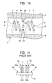
- a configuration of a known coupling adjusting structure for a double-tuned circuit will be described with reference to Fig. 11.
- a printed circuit board 51 has a variety of electrical components (not shown) disposed thereon including first and second tuned circuits 52 and 53 formed side by side.
- First and second coils 54 and 55 serving as a part of the first and second tuned circuits 52 and 53 have windings 54a and 55a formed by winding wires, and two pairs of fixing legs 54b and 55b disposed at the ends of the windings 54a and 55a, respectively.
- the first and second coils 54 and 55 are configured such that the windings 54a and 55a are mounted on the printed circuit board 51 in an upright manner while being close to each other, and the fixing legs 54b and 55b are passed through the printed circuit board 51 and soldered to corresponding conductive patterns (not shown) formed on the lower surface of the printed circuit board 51.
- an inductive coupling is adjusted by deforming free corresponding ends of the mutually opposing windings 54a and 55a of the first and second coils 54 and 55 in the opposing directions indicated by the arrows Z in the figure.
- the known coupling adjusting structure for a double-tuned circuit is configured such that the windings 54a and 55a are disposed in an upright manner against the printed circuit board 51 so as to deform a part of each of the windings 54a and 55a of the first and second coils 54 and 55, respectively, giving rise to a problem in that the double-tuned circuit is toll.
- a coupling adjusting structure for a double-tuned circuit comprises: a printed circuit board; a first tuned circuit comprising a first coil formed by a combination of first and second conductive patterns formed on first and second surfaces of the printed circuit board, respectively; and a second tuned circuit comprising a second coil formed by another combination of other first and second conductive patterns formed on the first and second surfaces of the printed circuit board, respectively.
- the first and second coils are configured such that the first conductive patterns formed on the first surface of the printed circuit board and the corresponding second conductive patterns formed on the second surface of the printed circuit board are connected to each other via corresponding connecting conductors, one end of the first coil and the corresponding end of the second coil are disposed close to each other, at least one first ground conductive pattern is disposed at least on the first surface of the printed circuit board, and at least one first jumper connected to the first ground conductive pattern is disposed between the first and second coils so as to adjust an inductive coupling of the double-tuned circuit.
- a first island conductive pattern which is out of conduction with the first ground conductive pattern is preferably provided between the first and second coils and on the first surface of the printed circuit, and the first jumper is preferably connected to the first ground conductive pattern and the first island conductive pattern.
- At least one second ground conductive pattern and a second island conductive pattern which lies between the first and second coils and which is out of conduction with the second ground conductive pattern are preferably provided on the second surface of the printed circuit board, the first and second ground conductive patterns are preferably connected to each other via a conductor, and the first and second island conductive patterns are preferably connected to each other via another conductor.
- At least one second jumper is preferably connected to the second ground conductive pattern and the second island conductive pattern so as to adjust the inductive coupling.
- a coupling adjusting structure for a double-tuned circuit comprises: a printed circuit board; a first tuned circuit comprising a first coil formed by a combination of first and second conductive patterns formed on first and second surfaces of the printed circuit board, respectively; and a second tuned circuit comprising a second coil formed by another combination of other first and second conductive patterns formed on the first and second surfaces of the printed circuit board, respectively.
- the first and second coils are configured such that the first conductive patterns formed on the first surface of the printed circuit board and the corresponding second conductive patterns formed on the second surface of the printed circuit board are connected to each other via corresponding connecting conductors, one end of the first coil and the corresponding end of the second coil are disposed close to each other, at least one first ground conductive pattern comprising a first adjusting conductive pattern extending between the first and second coils is disposed at least on the first surface of the printed circuit board, and the first adjusting conductive pattern is cut off by at least one first break so as to adjust an inductive coupling of the double-tuned circuit.
- At least one second ground conductive pattern comprising a second adjusting conductive pattern extending between the first and second coils is preferably provided on the second surface of the printed circuit board, and the first and second ground conductive patterns are preferably connected to each other via a conductor.
- the second adjusting conductive pattern is preferably cut off by at least one second break so as to adjust the inductive coupling.
- Fig. 1 is a plan view of a coupling adjusting structure for a double-tuned circuit according to a first embodiment of the present invention.
- Fig. 2 is a sectional view of the coupling adjusting structure taken along the line II-II indicated in Fig. 1.
- Fig. 3 is a plan view of another coupling adjusting structure for a double-tuned circuit according to a second embodiment of the present invention.
- Fig. 4 is a sectional view of the other coupling adjusting structure taken along the line IV-IV indicated in Fig. 3.
- Fig. 5 is a bottom view of the other coupling adjusting structure for a double-tuned circuit according to the second embodiment.
- a printed circuit board 1 is formed from a flat insulating plate and has a variety of electrical components (not shown) disposed thereon including first and second tuned circuits 2 and 3 formed side by side.
- a first coil 4 serving as a part of the first tuned circuit 2 has first conductive patterns 5 formed on a first surface of the printed circuit board 1, second conductive patterns 6 formed on a second surface of the printed circuit board 1, through-holes 1a perforated in the printed circuit board 1 so as to lie at mutually opposing ends of the first and second conductive patterns 5 and 6, and connecting conductors 7 filled in the through-holes 1a so as to connect the corresponding ends of the first and second conductive patterns 5 and 6 to each other.
- the first coil 4 is configured in a zigzag manner by the first and second conductive patterns 5 and 6. Also, the first conductive patterns 5 have end portions 5a and 5b, both connected to the first tuned circuit 2.
- a second coil 8 serving as a part of the second tuned circuit 3 has first conductive patterns 9 formed on the first surface of the printed circuit board 1, second conductive patterns 10 formed on the second surface of the printed circuit board 1, through-holes 1b perforated in the printed circuit board 1 so as to lie at mutually opposing ends of the first and second conductive patterns 9 and 10, and connecting conductors 11 filled in the through-holes 1b so as to connect the corresponding ends of the first and second conductive patterns 9 and 10 to each other.
- the second coil 4 is configured in a zigzag manner by the first and second conductive patterns 9 and 10. Also, the first conductive patterns 9 have end portions 9a and 9b, both connected to the second tuned circuit 3.
- one end of the first coil 4 and the corresponding end of the second coil 8 are disposed close to each other.
- first ground conductive patterns 12 and 13 so as to sandwich the first and second coils 4 and 8
- protruding conductive patterns 12a and 13a respectively extending from the first ground conductive patterns 12 and 13 so as to lie between the first and second coils 4 and 8
- a first island conductive pattern 14 which is disposed between the protruding conductive patterns 12a and 13a and which is out of conduction with the first ground conductive patterns 12 and 13.
- a first jumper 15 made from a conductor such as a metal plate or a metal wire is disposed by soldering so as to connect the protruding conductive pattern 12a of the first ground conductive pattern 12 and the first island conductive pattern 14.
- the first jumper 15 is disposed between the first and second coils 4 and 8 so as to adjust an inductive coupling between the first and second coils 4 and 8.
- another first jumper 15 may be disposed so as to connect the protruding conductive pattern 13a of the first ground conductive pattern 13 and the first island conductive pattern 14 as required.
- the inductive coupling of the double-tuned circuit having such a configuration is adjusted such that the degree of coupling between the first and second coils 4 and 8 is reduced by disposing the first jumper 15 between the first and second coils 4 and 8.
- Figs. 3 to 5 illustrate the other coupling adjusting structure for a double-tuned circuit according to the second embodiment of the present invention.
- a pair of second ground conductive patterns 16 and 17 having protruding conductive patterns 16a and 17a, respectively, which extend between the first and second coils 4 and 8, and also a second island conductive pattern 18 lying between the protruding conductive patterns 16a and 17a are provided on the second surface of the printed circuit board 1.
- the first ground conductive patterns 12 and 13 formed on the first surface of the printed circuit board 1 are respectively connected to the second ground conductive patterns 16 and 17 formed on the second surface of the printed circuit board 1 via corresponding conductors 19, and also the first and second island conductive patterns 14 and 18 respectively disposed on the first and second surfaces of the printed circuit board 1 are connected to each other via a conductor 20.
- the inductive coupling of the double-tuned circuit is adjusted by disposing a second jumper 15 so as to connect the protruding conductive pattern 16a and the second island conductive pattern 18 and/or by disposing another second jumper 15 so as to connect the protruding conductive pattern 17a and the second island conductive pattern 18.
- the inductive coupling can be adjusted in a further wider range.
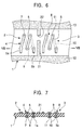
- Fig. 6 is a plan view of another coupling adjusting structure for a double-tuned circuit according to a third embodiment of the present invention.
- Fig. 7 is a sectional view of the other coupling adjusting structure taken along the line VII-VII indicated in Fig. 6.
- Fig. 8 is a plan view of another coupling adjusting structure for a double-tuned circuit according to a fourth embodiment of the present invention.
- Fig. 9 is a sectional view of the other coupling adjusting structure taken along the line IX-IX indicated in Fig. 8.
- Fig. 10 is a bottom view of the other coupling adjusting structure for a double-tuned circuit according to the fourth embodiment.
- the printed circuit board 1 is formed from a flat insulating plate and has a variety of electrical components (not shown) disposed thereon including the first and second tuned circuits 2 and 3 formed side by side.
- the first coil 4 serving as a part of the first tuned circuit 2 has the first conductive patterns 5 formed on the first surface of the printed circuit board 1, the second conductive patterns 6 formed on the second surface of the printed circuit board 1, the through-holes 1a perforated in the printed circuit board 1 so as to lie at the mutually opposing ends of the first and second conductive patterns 5 and 6, and the connecting conductors 7 filled in the through-holes 1a so as to connect the corresponding ends of the first and second conductive patterns 5 and 6 to each other.
- the first coil 4 is configured in a zigzag manner by the first and second conductive patterns 5 and 6. Also, the first conductive patterns 5 have the end portions 5a and 5b, each connected to the first tuned circuit 2.
- the second coil 8 serving as a part of the second tuned circuit 3 has the first conductive patterns 9 formed on the first surface of the printed circuit board 1, the second conductive patterns 10 formed on the second surface of the printed circuit board 1, the through-holes 1 perforated in the printed circuit board 1 so as to lie at the mutually opposing ends of the first and second conductive patterns 9 and 10, and the connecting conductors 11 filled in the through-holes 1b so as to connect the corresponding ends of the first and second conductive patterns 9 and 10 to each other.
- the second coil 8 is configured in a zigzag manner by the first and second conductive patterns 9 and 10. Also, the first conductive patterns 9 have the end portions 9a and 9b, each connected to the second tuned circuit 3.
- one end of the first coil 4 and the corresponding end of the second coil 8 are disposed close to each other.
- first ground conductive patterns 12 and 13 are provided so as to sandwich the first and second coils 4 and 8, and also a first adjusting conductive pattern 21 extending from the first ground conductive patterns 12 and 13 is provided so as to lie between the first and second coils 4 and 8, both on the first surface of the printed circuit board 1.
- the inductive coupling of the double-tuned circuit is adjusted such that the degree of coupling between the first and second coils 4 and 8 is increased by disposing a first break 22 which cuts off the first adjusting conductive pattern 21 lying between the first and second coils 4 and 8.
- the inductive coupling may be adjusted by providing a plurality of the breaks 22 for cutting the first adjusting conductive pattern 21 at a plurality of locations.
- Figs. 8 to 10 illustrate the other coupling adjusting structure for a double-tuned circuit according to the fourth embodiment of the present invention.
- the other pair of second ground conductive patterns 16 and 17 having a second adjusting conductive pattern 23 which lies between the first and second coils 4 and 8 are provided on the second surface of the printed circuit board 1, and the first ground conductive patterns 12 and 13 formed on the first surface of the printed circuit board 1 are respectively connected to the second ground conductive patterns 16 and 17 formed on the second surface via the corresponding conductors 19.
- the inductive coupling for a double-tuned circuit is adjusted such that the degree of coupling is increased by providing at least one second break 24 for cutting off the second adjusting conductive pattern 23, at least one location, lying between the first and second coils 4 and 8.
- the inductive coupling can be adjusted in a further wider range.
- the first and second coils 4 and 8 are formed by connecting the first conductive patterns 5 and 9 formed on the first surface of the printed circuit board 1 to the second conductive patterns 6 and 10 formed on the second surface of the printed circuit board 1 via the connecting conductors 7 and 11, respectively, thereby making the first and second coils 4 and 8 lower and thinner.
- the first ground conductive pattern 12 is disposed at least on the first surface of the printed circuit board 1 and the first jumper 15 connected to the first ground conductive pattern 12 is disposed between the first and the second coils 4 and 8 so as to adjust the inductive coupling, while one end of the first coil 4 and the corresponding end of the second coil 8 are disposed close to each other, thereby achieving a double-tuned circuit which can adjust the inductive coupling.
- the first island conductive pattern 14 which is out of conduction with the first ground conductive patter 12, is formed between the first and second coils 4 and 8, and the first jumper 15 is connected to the first ground conductive pattern 12 and the first island conductive pattern 14, thereby achieving the first jumper 15 which can be connected easily and has a large strength of connection.
- the second ground conductive pattern 16 and the second island conductive pattern 18, which lies between the first and second coils 4 and 8 and is out of conduction with the second ground conductive pattern 16, are provided on the second surface of the printed circuit board 1, the first and second ground conductive patterns 12 and 16 are connected to each other via the corresponding conductor 19, and also the first and second island conductive patterns 14 and 18 are connected to each other via the conductor 20, whereby each of the former and latter groups of the connected conductive patterns has the same electric potential and also the inductive couplings can be adjusted on both surfaces of the printed circuit board 1.
- the second ground conductive pattern 16 and the second island conductive pattern 18 are connected to each other via the second jumper 15 so as to adjust the inductive coupling, thereby achieving the second jumper 15 which can be connected easily and has a large strength of connection, and allowing the inductive coupling to be adjusted in a wider range.
- the first and second coils 4 and 8 are formed such that the first conductive patterns 5 and 9 formed on the first surface of the printed circuit board 1 and the second conductive patterns 6 and 10 formed on the second surface of the printed circuit board 1 are respectively connected to each other via the connecting conductors 7 and 11, thereby making the first and second coils 4 and 8 lower and thinner.
- the first adjusting conductive pattern 21 connected to the first ground conductive pattern 12 is disposed at least on the first surface of the printed circuit board 1 and the first adjusting conductive pattern 21 is cut off by the first break 22 so as to adjust the inductive coupling, while one end of the first coil 4 is disposed close to the corresponding end of the second coil 8, thereby achieving a double-tuned circuit whose inductive coupling can be easily adjusted.
- the second ground conductive pattern 16 is provided on the second surface of the printed circuit board 1, and the first and second ground conductive patterns 12 and 16 are connected to each other via the corresponding conductor 19, whereby each of the connected conductive patterns and conductor has the same electric potential and also the inductive couplings can be adjusted on both surfaces of the printed circuit board 1.
- the second adjusting conductive pattern 23 is cut off by the second break 24 so as to adjust the inductive coupling, thereby allowing the inductive coupling to be adjusted in a further wider range.
Landscapes
- Engineering & Computer Science (AREA)
- Microelectronics & Electronic Packaging (AREA)
- Power Engineering (AREA)
- Multimedia (AREA)
- Signal Processing (AREA)
- Coils Or Transformers For Communication (AREA)
Applications Claiming Priority (4)
| Application Number | Priority Date | Filing Date | Title |
|---|---|---|---|
| JP2001249508 | 2001-08-20 | ||
| JP2001249509A JP4397134B2 (ja) | 2001-08-20 | 2001-08-20 | 複同調回路の結合調整構造 |
| JP2001249508A JP3936562B2 (ja) | 2001-08-20 | 2001-08-20 | 複同調回路の結合調整構造 |
| JP2001249509 | 2001-08-20 |
Publications (2)
| Publication Number | Publication Date |
|---|---|
| EP1286464A1 true EP1286464A1 (fr) | 2003-02-26 |
| EP1286464B1 EP1286464B1 (fr) | 2004-05-19 |
Family
ID=26620682
Family Applications (1)
| Application Number | Title | Priority Date | Filing Date |
|---|---|---|---|
| EP02018186A Expired - Lifetime EP1286464B1 (fr) | 2001-08-20 | 2002-08-19 | Structure d' ajustage de couplage inductif de circuits électriques |
Country Status (3)
| Country | Link |
|---|---|
| US (2) | US6784780B2 (fr) |
| EP (1) | EP1286464B1 (fr) |
| KR (1) | KR100436838B1 (fr) |
Cited By (2)
| Publication number | Priority date | Publication date | Assignee | Title |
|---|---|---|---|---|
| GB2404091A (en) * | 2003-07-15 | 2005-01-19 | Motorola Inc | Circuit board having first and second inductors mounted on either side of the board |
| EP1955343A4 (fr) * | 2005-11-30 | 2009-07-22 | Avocent Corp | Ligne a retard a solenoide multicouche sur circuit imprime |
Families Citing this family (5)
| Publication number | Priority date | Publication date | Assignee | Title |
|---|---|---|---|---|
| JP2005201716A (ja) * | 2004-01-14 | 2005-07-28 | Honda Motor Co Ltd | 電流検出装置、及び蓄電装置の制御装置 |
| DE102004047650B3 (de) * | 2004-09-30 | 2006-04-13 | W.L. Gore & Associates Gmbh | Kleidungsstück mit induktivem Koppler und induktive Bekleidungsstückschnittstelle |
| JP3108714U (ja) * | 2004-11-11 | 2005-04-28 | アルプス電気株式会社 | テレビジョンチューナの中間周波回路 |
| JP4411354B2 (ja) * | 2008-07-02 | 2010-02-10 | アルプス電気株式会社 | 複同調回路 |
| JP7787730B2 (ja) * | 2022-02-08 | 2025-12-17 | Tdk株式会社 | 積層型フィルタ |
Citations (5)
| Publication number | Priority date | Publication date | Assignee | Title |
|---|---|---|---|---|
| DD132226A1 (de) * | 1977-05-31 | 1978-09-06 | Matthias Lindner | Induktivitaeten auf schichtfoermigen leitungstraegern |
| JPH01135234A (ja) * | 1987-11-20 | 1989-05-26 | Fujitsu General Ltd | 衛星放送テレビ受信機のチューナ回路 |
| EP0497556A1 (fr) * | 1991-01-30 | 1992-08-05 | Sharp Kabushiki Kaisha | Dispositif de bobine imprimée pour circuit d'accord double |
| JPH04290005A (ja) * | 1991-03-19 | 1992-10-14 | Matsushita Electric Ind Co Ltd | 可変インダクタンスと、この可変インダクタンスを用いた共振回路と、この共振回路を用いたフィルタと、このフィルタを用いた高周波装置 |
| JPH10303026A (ja) * | 1997-04-23 | 1998-11-13 | Nec Home Electron Ltd | コイル |
Family Cites Families (4)
| Publication number | Priority date | Publication date | Assignee | Title |
|---|---|---|---|---|
| DE132226C (fr) | ||||
| JPS5319386B2 (fr) * | 1972-11-14 | 1978-06-20 | ||
| US3820045A (en) * | 1972-11-20 | 1974-06-25 | Alps Electric Co Ltd | Double-tuned circuit device |
| US5777277A (en) * | 1995-09-21 | 1998-07-07 | Canon Kabushiki Kaisha | Printed circuit board |
-
2002
- 2002-08-13 US US10/217,557 patent/US6784780B2/en not_active Expired - Fee Related
- 2002-08-19 KR KR10-2002-0048883A patent/KR100436838B1/ko not_active Expired - Fee Related
- 2002-08-19 EP EP02018186A patent/EP1286464B1/fr not_active Expired - Lifetime
-
2003
- 2003-09-25 US US10/670,687 patent/US6864776B2/en not_active Expired - Lifetime
Patent Citations (5)
| Publication number | Priority date | Publication date | Assignee | Title |
|---|---|---|---|---|
| DD132226A1 (de) * | 1977-05-31 | 1978-09-06 | Matthias Lindner | Induktivitaeten auf schichtfoermigen leitungstraegern |
| JPH01135234A (ja) * | 1987-11-20 | 1989-05-26 | Fujitsu General Ltd | 衛星放送テレビ受信機のチューナ回路 |
| EP0497556A1 (fr) * | 1991-01-30 | 1992-08-05 | Sharp Kabushiki Kaisha | Dispositif de bobine imprimée pour circuit d'accord double |
| JPH04290005A (ja) * | 1991-03-19 | 1992-10-14 | Matsushita Electric Ind Co Ltd | 可変インダクタンスと、この可変インダクタンスを用いた共振回路と、この共振回路を用いたフィルタと、このフィルタを用いた高周波装置 |
| JPH10303026A (ja) * | 1997-04-23 | 1998-11-13 | Nec Home Electron Ltd | コイル |
Non-Patent Citations (3)
| Title |
|---|
| PATENT ABSTRACTS OF JAPAN vol. 013, no. 386 (E - 812) 25 August 1989 (1989-08-25) * |
| PATENT ABSTRACTS OF JAPAN vol. 017, no. 101 (E - 1327) 2 March 1993 (1993-03-02) * |
| PATENT ABSTRACTS OF JAPAN vol. 1999, no. 02 26 February 1999 (1999-02-26) * |
Cited By (4)
| Publication number | Priority date | Publication date | Assignee | Title |
|---|---|---|---|---|
| GB2404091A (en) * | 2003-07-15 | 2005-01-19 | Motorola Inc | Circuit board having first and second inductors mounted on either side of the board |
| GB2404091B (en) * | 2003-07-15 | 2005-08-17 | Motorola Inc | Circuit board constructions |
| EP1955343A4 (fr) * | 2005-11-30 | 2009-07-22 | Avocent Corp | Ligne a retard a solenoide multicouche sur circuit imprime |
| US8031033B2 (en) | 2005-11-30 | 2011-10-04 | Avocent Corporation | Printed multilayer solenoid delay line having at least two sub-sets with different patterns |
Also Published As
| Publication number | Publication date |
|---|---|
| EP1286464B1 (fr) | 2004-05-19 |
| KR20030016181A (ko) | 2003-02-26 |
| KR100436838B1 (ko) | 2004-06-22 |
| US6784780B2 (en) | 2004-08-31 |
| US20030034868A1 (en) | 2003-02-20 |
| US20040058593A1 (en) | 2004-03-25 |
| US6864776B2 (en) | 2005-03-08 |
Similar Documents
| Publication | Publication Date | Title |
|---|---|---|
| US4661792A (en) | Apparatus for mounting printed circuit boards | |
| EP1286464B1 (fr) | Structure d' ajustage de couplage inductif de circuits électriques | |
| US6949819B2 (en) | Jumper chip component and mounting structure therefor | |
| JPH07272934A (ja) | プリント基板 | |
| EP0301789A1 (fr) | Filtre demi-onde à couplage latéral | |
| EP0865048A1 (fr) | Transformateur à coût réduit empilable avec filtres EMI encastrés | |
| US6888227B2 (en) | Apparatus for routing signals | |
| US5416274A (en) | Circuit board | |
| JP3530663B2 (ja) | プリントインダクタ | |
| JP3115597U (ja) | 面実装用トランス | |
| JP3936562B2 (ja) | 複同調回路の結合調整構造 | |
| JP4397134B2 (ja) | 複同調回路の結合調整構造 | |
| JP3917850B2 (ja) | 結合回路 | |
| JP2000012130A (ja) | コネクタ構造 | |
| JP4160948B2 (ja) | アンテナ装置 | |
| JPH0550708U (ja) | シートコイル装置 | |
| JP2008135808A (ja) | アンテナと、このアンテナを用いたアンテナ装置、およびこのアンテナ装置の製造方法 | |
| JP3430964B2 (ja) | Lcフィルタ | |
| EP0854541A1 (fr) | Connecteur et circuit pour des courants forts | |
| JPH06232522A (ja) | 印刷配線基板 | |
| JPH06334290A (ja) | ジャンパ線の立体配置構造 | |
| JPH08172246A (ja) | フレキシブル配線基板の構造 | |
| JPH0992952A (ja) | プリントパターン素子 | |
| JP2008135429A (ja) | インダクタと、このインダクタを用いた高周波装置、およびこの高周波装置の製造方法 | |
| JPH05326295A (ja) | 平面型トランス |
Legal Events
| Date | Code | Title | Description |
|---|---|---|---|
| PUAI | Public reference made under article 153(3) epc to a published international application that has entered the european phase |
Free format text: ORIGINAL CODE: 0009012 |
|
| AK | Designated contracting states |
Designated state(s): AT BE BG CH CY CZ DE DK EE ES FI FR GB GR IE IT LI LU MC NL PT SE SK TR Kind code of ref document: A1 Designated state(s): AT BE BG CH CY CZ DE DK EE ES FI FR GB GR IE IT LI LU MC NL PT SE SK TR |
|
| AX | Request for extension of the european patent |
Extension state: AL LT LV MK RO SI |
|
| 17P | Request for examination filed |
Effective date: 20030318 |
|
| GRAP | Despatch of communication of intention to grant a patent |
Free format text: ORIGINAL CODE: EPIDOSNIGR1 |
|
| AKX | Designation fees paid |
Designated state(s): FR GB |
|
| REG | Reference to a national code |
Ref country code: DE Ref legal event code: 8566 |
|
| GRAS | Grant fee paid |
Free format text: ORIGINAL CODE: EPIDOSNIGR3 |
|
| GRAA | (expected) grant |
Free format text: ORIGINAL CODE: 0009210 |
|
| AK | Designated contracting states |
Kind code of ref document: B1 Designated state(s): FR GB |
|
| REG | Reference to a national code |
Ref country code: GB Ref legal event code: FG4D |
|
| REG | Reference to a national code |
Ref country code: IE Ref legal event code: FG4D |
|
| ET | Fr: translation filed | ||
| PLBE | No opposition filed within time limit |
Free format text: ORIGINAL CODE: 0009261 |
|
| STAA | Information on the status of an ep patent application or granted ep patent |
Free format text: STATUS: NO OPPOSITION FILED WITHIN TIME LIMIT |
|
| 26N | No opposition filed |
Effective date: 20050222 |
|
| REG | Reference to a national code |
Ref country code: IE Ref legal event code: MM4A |
|
| PGFP | Annual fee paid to national office [announced via postgrant information from national office to epo] |
Ref country code: GB Payment date: 20060830 Year of fee payment: 5 |
|
| GBPC | Gb: european patent ceased through non-payment of renewal fee |
Effective date: 20070819 |
|
| PG25 | Lapsed in a contracting state [announced via postgrant information from national office to epo] |
Ref country code: GB Free format text: LAPSE BECAUSE OF NON-PAYMENT OF DUE FEES Effective date: 20070819 |
|
| PGFP | Annual fee paid to national office [announced via postgrant information from national office to epo] |
Ref country code: FR Payment date: 20090806 Year of fee payment: 8 |
|
| REG | Reference to a national code |
Ref country code: FR Ref legal event code: ST Effective date: 20110502 |
|
| PG25 | Lapsed in a contracting state [announced via postgrant information from national office to epo] |
Ref country code: FR Free format text: LAPSE BECAUSE OF NON-PAYMENT OF DUE FEES Effective date: 20100831 |