EP1288968A2 - Festzustandspeicher - Google Patents
Festzustandspeicher Download PDFInfo
- Publication number
- EP1288968A2 EP1288968A2 EP02255084A EP02255084A EP1288968A2 EP 1288968 A2 EP1288968 A2 EP 1288968A2 EP 02255084 A EP02255084 A EP 02255084A EP 02255084 A EP02255084 A EP 02255084A EP 1288968 A2 EP1288968 A2 EP 1288968A2
- Authority
- EP
- European Patent Office
- Prior art keywords
- address
- level
- elements
- lines
- memory
- Prior art date
- Legal status (The legal status is an assumption and is not a legal conclusion. Google has not performed a legal analysis and makes no representation as to the accuracy of the status listed.)
- Withdrawn
Links
- 239000007787 solid Substances 0.000 title claims abstract description 14
- 230000002950 deficient Effects 0.000 claims abstract description 19
- 230000007547 defect Effects 0.000 claims description 17
- 238000000034 method Methods 0.000 claims description 9
- 238000004519 manufacturing process Methods 0.000 claims description 6
- 230000001678 irradiating effect Effects 0.000 claims description 3
- 239000000976 ink Substances 0.000 abstract 1
- 230000005670 electromagnetic radiation Effects 0.000 description 10
- 230000005855 radiation Effects 0.000 description 7
- 229910021417 amorphous silicon Inorganic materials 0.000 description 5
- 230000006870 function Effects 0.000 description 5
- 238000007726 management method Methods 0.000 description 5
- 239000000463 material Substances 0.000 description 5
- 238000012937 correction Methods 0.000 description 3
- 239000000758 substrate Substances 0.000 description 3
- 238000013459 approach Methods 0.000 description 2
- 238000007664 blowing Methods 0.000 description 2
- 230000003287 optical effect Effects 0.000 description 2
- 238000012545 processing Methods 0.000 description 2
- 238000003491 array Methods 0.000 description 1
- 229910021419 crystalline silicon Inorganic materials 0.000 description 1
- 238000013500 data storage Methods 0.000 description 1
- 238000013461 design Methods 0.000 description 1
- 238000010586 diagram Methods 0.000 description 1
- 239000004973 liquid crystal related substance Substances 0.000 description 1
- 238000013507 mapping Methods 0.000 description 1
- 230000000873 masking effect Effects 0.000 description 1
- 238000004806 packaging method and process Methods 0.000 description 1
- 229920001690 polydopamine Polymers 0.000 description 1
- 239000004065 semiconductor Substances 0.000 description 1
- 230000035939 shock Effects 0.000 description 1
- 229910052710 silicon Inorganic materials 0.000 description 1
- 239000010703 silicon Substances 0.000 description 1
- 238000012546 transfer Methods 0.000 description 1
Images


Classifications
-
- G—PHYSICS
- G11—INFORMATION STORAGE
- G11C—STATIC STORES
- G11C29/00—Checking stores for correct operation ; Subsequent repair; Testing stores during standby or offline operation
- G11C29/70—Masking faults in memories by using spares or by reconfiguring
- G11C29/78—Masking faults in memories by using spares or by reconfiguring using programmable devices
Definitions
- the present invention relates to information storage devices. More specifically, the present invention relates to one-time programmable (OTP) solid state memory and in particular to a fault-tolerant memory.
- OTP one-time programmable
- Portable devices such as PDAs, handheld computers, digital cameras and digital music players include memory for storing data, digital images and MP3 files.
- Different types of memory are available for these portable devices.
- Conventional memory types include flash memory, mini-hard drives, mini-compact discs, and magnetic tape.
- each of these memory types has one or more of the following limitations: large physical size, low storage capacity, relatively high cost, poor robustness, slow access time and high power consumption.
- a solid state diode-based OTP memory is disclosed in European patent application 02253896.1. Compared to the conventional memory, the diode-based memory has a high shock tolerance, low power consumption, fast access time, moderate transfer rate and good storage capacity.
- the diode-based memory can fit into a standard portable interface (e.g., PCMCIA, CF) of a portable device.
- Address logic of the diode-based memory device is formed on the same level as main memory.
- each level has main memory and address logic (unlike conventional solid state memory such as DRAM).
- the address logic of the diode-based memory device is programmable. The address logic may be programmed after each layer has been fabricated. Since no masking is required, physical processing is simplified. Defective areas in the address logic and main memory can occur during manufacture. These defective areas can render certain memory elements unusable.
- a solid state memory device is fabricated by forming a level of the device; identifying defective areas in the level; and programming address logic of the level to avoid the defective areas in the level.
- Figure 1 is a block diagram of a level of a solid state memory device.
- Figures 2a-2c are illustrations of different types of programmable elements in the level.
- Figure 3 is another illustration of a programmable element.
- Figure 4 is an illustration of a method of changing the resistance states of address elements.
- Figures 5a-5c are illustrations of different layouts for selected and unselected address elements of a decoder.
- Figures 6a and 6b are illustrations of a level of a solid state memory device that allows for defect management.
- Figure 7 is an illustration of a method of avoiding defects in a multi-level solid state memory device.
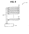
- Figure 8 is an illustration of a multi-level solid state memory device.
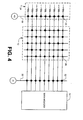
- FIG. 1 shows a level 8 of a solid state memory device.
- the level 8 includes main memory 10 and programmable address logic 12, 14.
- the main memory 10 includes a cross point resistive array of OTP memory elements 16, traces functioning as word lines 18 extending along rows of the memory elements 16, and traces functioning as bit lines 20 extending along columns of the memory elements 16. There may be one word line 18 for each row of the memory elements 16 and one bit line 20 for each column of memory elements 16.
- Each memory element 16 is located at a cross point of a word line 18 and a bit line 20. Only a relatively small number of memory elements 16 is shown to simplify the illustration of the level 8. In practice, arrays of any size may be used.
- the address logic 12, 14 uses combinational diode logic for addressing the memory elements 16 during read and write operations.
- the address logic 12, 14 includes an OTP row decoder 12 for selecting the word lines 18.
- the row decoder 12 selects the word lines 18 by decoding addresses supplied on row address lines 22 (the addresses may be supplied by external row address drivers 24).
- the row decoder 12 includes a plurality of OTP address elements 26. Each address element 26 of the row decoder 12 is at a cross point of a word line 18 and a row address line 22.
- the address logic 12, 14 also includes an OTP column decoder 14 for selecting the bit lines 20.
- the column decoder 14 selects the bit lines 20 by decoding addresses supplied on column address lines 28 (the addresses may be supplied by external column address drivers 30).
- the column decoder 14 also includes a plurality of OTP address elements 26. Each address element 26 of the column decoder 14 is at the cross point of a bit line 20 and a column address line 28.
- each word line 18 terminates at row sense logic 34.
- the row sense logic 34 includes multiple sense resistors 36, each sense resistor 36 connected between a row power line 38 and an end of a word line 18.
- a row sense line 40 crosses the word lines 18.
- the row sense logic 34 also includes multiple sense elements 42, each sense element 42 connected between the row sense line 40 and a word line 18.
- each bit line 20 terminates at column sense logic 44.
- the column sense logic 44 includes multiple sense resistors 36, each sense resistor 36 connected between a column power line 46 and an end of a bit line 20.
- a column sense line 48 crosses the bit lines 20.
- the column sense logic 44 also includes multiple sense elements 42, each sense element 42 connected between the column sense line 48 and a bit line 20.
- a row programming line 50 between the main memory 10 and the row decoder 12, crosses the word lines 18.
- Programming elements 52 are connected between the row programming line 50 and the word lines 18.
- a column programming line 54 between the main memory 10 and the column decoder 14, crosses the bit lines 20.
- Programming elements 52 are connected between the column programming line 54 and the bit lines 20.
- the memory elements 16, the address elements 26, the sense elements 42 and the programming elements 52 may all be diode based. This simplifies the fabrication of the level 8.
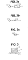
- the programmable element of Figure 2a includes a fuse 110 coupled in series with a diode 112. Prior to programming, the resistance state of such an element is low, with the fuse 110 intact. During programming, the resistance state of the element can be changed from low to high by "blowing" the fuse 110.
- the programmable element of Figure 2b includes a resistor 120 coupled in series with a diode 122. Prior to programming, the resistance state of such an element is low, with the resistor 120 intact. During programming, the resistance state of the element can be changed from low to high by "blowing" the resistor 120.
- the programmable element of Figure 2c includes only a diode 132. Prior to programming, the diode 132 is intact, whereby its resistance state is low. During programming, the diode 132 can be opened to change its resistance state from low to high. Such a diode 132 functions as a fuse. In the alternative, the diode 132 can function as an anti-fuse, going from a high resistance state to a low resistance state during programming.
- the programmable elements 16/26/42/52 are not limited to the types shown in Figures 2a-2c.
- the programmable elements 16/26/42/52 could include transistors instead of diodes.
- the level 8 may be fabricated as follows. Column lines 20 are formed on a substrate, a multi-layer film of silicon is formed on the column lines 20, and word lines 18 are formed on the film.
- Each programmable element 16/26/42/52 may be formed as that portion of the film (F) between two crossing traces (T) (see Figure 3). The size of the programmable element 16/26/42/52 is determined by the overlapping area between crossing traces and the thickness of the film. For example, a diode in main memory 10 is formed as that portion of the film between crossing word and bit lines 18 and 20.
- the different layers of the film have appropriate dopings (and/or a combination of crystalline and amorphous silicon) to form the diodes 112, 122, 132. Additional layers with appropriate dopings can be added to form resistors 120, fuses 110, or anti-fuses.
- the sense resistors 36 may be formed by modifying the ends of the word and bit lines 18 and 20.
- the row and column address drivers 24 and 30 may be formed on the substrate.
- the row and column decoders 12 and 14 may be programmed during device fabrication, after the level 8 has been fabricated.
- the decoders 12 and 14 are programmed by changing the resistance states of selected address elements from a low resistance state to a high resistance state (or vice versa). Details of the combinational logic for addressing the main memory (that is, the details about which address elements are selected) are disclosed in European patent application 02253896.1. Various ways of programming the decoders 12 and 14 will be described below.
- Data may be written to the main memory 10 by supplying row and column addresses to the row and column decoders 12 and 14.
- a write current flows through a selected word line 18 and a selected bit line 20 and, therefore, flows through the memory element 16 at the cross point of the selected word and bit lines 18 and 20.
- Magnitude of the write current is sufficient to change the resistance state of the selected element (e.g., by opening the fuse 110 of Figure 2a, opening the resistor 120 of Figure 2b, opening the diode 132 of Figure 2c, shorting the anti-fuse).
- the resistance state of a memory element 16 may be sensed by supplying row and column addresses to the row and column decoders 12 and 14. A voltage is applied to the second row sense line 40 and a voltage of opposite polarity is applied to the second column sense line 48. A sense current flows through a selected word line 18 and a selected bit line 20 and, therefore, flows through the memory element 16 at the cross point of the selected word and bit lines 18 and 20. Magnitude of the sense current indicates the resistance state of the selected memory element 16.
- Each address element 26 has a link that may be broken during programming.
- the fuse 110 is the link for the address element shown in Figure 2a, the resistor 120 for the address element of Figure 2b, and the diode 132 for the address element of Figure 2c.
- Each link is made of a photosensitive material typically used for solar cells and displays.
- the links may be made of amorphous silicon with a P-doped layer.
- the conductivity of intrinsic amorphous silicon is typically 10 6 times lower than the doped amorphous silicon. However, when irradiated with light, the conductivity of the intrinsic region increases to a level similar to that of the doped region.
- density of current flowing through the address element 26 is increased to the point that the link blows.
- FIG 4 illustrates a method of changing the resistance state of "selected" address elements 26.
- Address elements that are selected are indicated by X's. These selected elements will have their resistance states changed during programming.
- Unselected address elements are indicated by O's. These unselected address elements will not have their resistance states changed during programming.
- a voltage (-V) is applied across the row programming line 50, and a voltage of opposite polarity (+V) is applied to the row sense line 40.
- a voltage is applied across the column programming line 54, and a voltage of opposite polarity is applied to the column sense line 48.
- This will effectively apply a voltage across two diodes connected back-to-back.
- the voltage is applied in such a manner that the diodes in the programming elements 52 are forward biased and the diodes in the address elements 26 are reverse biased.
- the voltages can be applied by the row and column address drivers 24 and 30.
- Electromagnetic radiation is applied to the selected address elements 26.
- the electromagnetic radiation is of sufficient intensity to significantly increase the conductivity of the selected address elements. Consequently, the density of the current flowing through the selected address elements is increased. This increase in current density causes the links of the selected address elements to open. The links of the unselected address elements remain unbroken.
- the programming elements 52 may have a higher current-carrying capability than the selected address elements 26.
- This optical programming of the address diodes 26 may be performed by using a jig including addressable laser diodes.
- the laser diodes irradiate only the selected address elements 26.
- Lenses and other optical elements may be used to focus the EM radiation on the selected address elements 26. All selected elements 26 may be irradiated simultaneously, whereby the resistance states of all selected address elements 26 are changed at the same time.
- the unselected address elements could be masked from the irradiation, and blanket irradiation could be applied to the layer. Resistance states of the masked address elements would not be changed.
- the traces may be made transparent to the EM radiation. Materials for these transparent traces may be of the type used in liquid crystal displays. As an alternative to making transparent traces, the EM radiation may be guided to the selected address elements 26.
- the unselected address elements in each decoder 12 and 14 are formed with a greater current-carrying capability than the selected address elements 26.
- all address elements are reversed-biased and the sense elements are forward-biased in the manner described above. Consequently, a current flows through the selected and unselected address elements. This current causes the links of the selected address elements 26 to break, but the current does not cause the links of the unselected selected address elements to break.
- the links may be broken without applying EM radiation to the selected address elements 26. Therefore, the links may be made of a material that is not photoconductive. However, reliability in breaking the links may be increased by making the links from a photoconductive material and irradiating the selected address elements 26 during programming.
- the memory elements 16 and the selected address elements 26 may be made at the minimum resolution, thus allowing the optimal storage capacity.
- the unselected address elements may be made with larger dimensions by increasing the size of the address lines above the minimum resolution and increasing those portions of the memory lines (i.e., word and bit lines) that cross the address lines.
- Figures 5a-5c show different layouts for selected address elements 26a and enlarged, unselected address elements 26b. If an address protocol can guarantee that no column has adjacent enlarged (unselected) address elements 26b, then the address logic may have the configuration shown in Figure 5a.
- Figure 5a shows a row decoder 12 in which columns do not contain any adjacent enlarged (unselected) address elements 26b. Although not shown as such, the address elements 26a and 26b may be formed at full contact pitch.
- the address protocol cannot provide such a guarantee, whereby the address logic could include adjacent enlarged address elements in a column, the distance between word lines 18 may be increased. However, this would reduce the data storage density of the main memory.
- the row decoder 12 may be divided into two spaced-apart sets 12a and 12b, as shown in Figure 5b. Odd-numbered word lines 18a are interdigitated with even-numbered word lines 18b. A first set of address lines 22a crosses the odd-numbered word lines 18a, and a second set of address lines 22b crosses the even-numbered word lines 18b. The first and second sets of address lines 22a and 22b receive the same address signal.
- FIGS 5a-5c were just described in connection with the row decoder 12. However, the same principles can be applied to the column decoder 14.
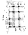
- the level 208 includes main memory 210, a row decoder 212, and row sense logic 234.
- the row sense logic 234 includes sense resistors 236.
- the level 208 further includes word lines 218, bit lines 220, row address lines 222, a power supply line 238, a row sense line 240, and a row programming line 242. Elements for addressing, sensing and programming on the column side are not shown. Selected address elements are indicated by X's and unselected address elements are indicated by O's.
- a defective area in the level 8 is identified by the letter D.
- the defective area D might be caused by a short of two adjacent word lines 218.
- the defective area D renders the two associated rows unusable.
- the row decoder 212 can be programmed to avoid the defective area D.
- the word lines 218 corresponding to the defective area D are disconnected from main memory 210. For example, breaks (discontinuities) may be formed in these word lines 218.
- the sense resistors 236 of these word lines 218 may be opened. If the sense resistors 236 are made from a photoconductive material such as amorphous silicon, they can be opened or "blown" by causing a current to flow through the resistors (e.g., by biasing the address and write lines with respect to the drive voltage) and then applying EM radiation. Applying the EM radiation increases the conductivity. The increase in current causes the irradiated sense resistor to be blown.
- the disconnected word lines are replaced by spare word lines.
- Certain word lines and their connected memory, address and sense elements are reserved as spares.
- Figure 6a shows that the last few word lines of the level 208 are reserved as spares (as indicated by the block 211). However, the location of the spares are not so limited; the spare word lines may be at any location in the level 208. Initially, all address elements connected to the spares are unselected .
- the spare word lines have additional logic 252.
- Each address line 254 is connected to a corresponding spare word line by a spare address element 256.
- the encoding may be performed by optically programming the selected spare address elements 256.
- Figure 6b shows the decoder 212 re-mapped to avoid the defective area D.
- the two word lines 218a and 218b associated with the defective area D are disconnected by opening their sense resistors 236.
- Two spare lines 218c and 218d replace the two lines 218a and 218b that were disconnected.
- the address elements 256 connected to these two replacement spare lines 218c and 218d have been programmed to match the resistance states of selected and unselected address elements for the two disconnected lines 218a and 218b.
- these two replacement spare lines 218c and 218d now have the same addresses as the disconnected word lines 218a and 218b.
- the spare address elements connected to these two replacement spare lines 218c and 218d are changed to a high resistance state and, thus, effectively removed from the row decoder 212.
- the unused spare line 218e is disconnected by opening its sense resistor 236.
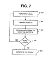
- FIG. 7 illustrates a method of fabricating a multi-level solid state memory device.
- defects in the first level are identified (block 304). Such defects include, but are not limited to, discontinuities or defects in one or both cross point wires, and shorts between data lines.
- the defects may be identified by measuring I-V characteristics of each cross point in main memory.
- the decoders are programmed to avoid a significant number of the defects (block 306).
- the programming reduces the defect level to zero or an acceptable level for error correction (that is, a level that does not stress or overload error correction).
- Subsequent levels are formed (block 308). Each time a level is formed (block 302), defects in the level are identified (block 304), and the decoders on that level are programmed to avoid the defects (block 306).
- the memory device is completed (block 310). As part of completing the memory device, address lines are connected, interface circuitry is added and the levels are packaged.
- This method allows defect management to be implemented on individual levels and therefore avoids the problem of a defective area in one level eliminating the use of the same memory area of another level. It also implements defect management in a manner that physically re-positions the defective address location and therefore does not require a defect list for re-mapping. This simplifies use of the memory system.
- FIG 8 shows a multi-level solid state memory device 410.
- Multiple levels 412 are stacked on top of one another.
- decoders are formed in each layer 412.
- Each layer 410 is connected to control/interface circuitry 414 by a memory system interface 416.
- the control/interface circuitry 414 is formed in the substrate.
- the control/interface circuitry 414 performs error code correction (ECC) and defect management functions, as well as functions for operating the device 410. These functions include setting write voltages, setting write enable lines and controlling power sense striping, addressing the memory by converting logical addresses to address line patterns required to access physical memory locations, and data read processing of sense line outputs.
- ECC error code correction
- the device 410 is not limited to control/interface circuitry that is shared by the layers. Instead each level 412 may have its own control/interface circuitry.
- the main memory could be programmed at the factory, in the same manner and at the same time as the address logic.
- the main memory might be pre-programmed with microcode, map data, etc.
Landscapes
- Read Only Memory (AREA)
- Semiconductor Memories (AREA)
- For Increasing The Reliability Of Semiconductor Memories (AREA)
- Techniques For Improving Reliability Of Storages (AREA)
Applications Claiming Priority (2)
| Application Number | Priority Date | Filing Date | Title |
|---|---|---|---|
| US09/911,968 US6744681B2 (en) | 2001-07-24 | 2001-07-24 | Fault-tolerant solid state memory |
| US911968 | 2001-07-24 |
Publications (2)
| Publication Number | Publication Date |
|---|---|
| EP1288968A2 true EP1288968A2 (de) | 2003-03-05 |
| EP1288968A3 EP1288968A3 (de) | 2004-10-27 |
Family
ID=25431188
Family Applications (1)
| Application Number | Title | Priority Date | Filing Date |
|---|---|---|---|
| EP02255084A Withdrawn EP1288968A3 (de) | 2001-07-24 | 2002-07-19 | Festzustandspeicher |
Country Status (6)
| Country | Link |
|---|---|
| US (2) | US6744681B2 (de) |
| EP (1) | EP1288968A3 (de) |
| JP (1) | JP2003124441A (de) |
| KR (1) | KR20030011601A (de) |
| CN (1) | CN1316505C (de) |
| TW (1) | TW556208B (de) |
Families Citing this family (11)
| Publication number | Priority date | Publication date | Assignee | Title |
|---|---|---|---|---|
| US5673218A (en) | 1996-03-05 | 1997-09-30 | Shepard; Daniel R. | Dual-addressed rectifier storage device |
| US6956757B2 (en) * | 2000-06-22 | 2005-10-18 | Contour Semiconductor, Inc. | Low cost high density rectifier matrix memory |
| US7003713B2 (en) * | 2002-05-16 | 2006-02-21 | Broadcom Corporation | Variable Hamming error correction for a one-time-programmable-ROM |
| JP4892215B2 (ja) * | 2005-09-28 | 2012-03-07 | 富士通セミコンダクター株式会社 | 半導体記憶装置 |
| US7898882B2 (en) * | 2006-06-23 | 2011-03-01 | Synopsys, Inc. | Architecture, system and method for compressing repair data in an integrated circuit (IC) design |
| US7630246B2 (en) * | 2007-06-18 | 2009-12-08 | Micron Technology, Inc. | Programming rate identification and control in a solid state memory |
| US7813157B2 (en) * | 2007-10-29 | 2010-10-12 | Contour Semiconductor, Inc. | Non-linear conductor memory |
| US20090225621A1 (en) * | 2008-03-05 | 2009-09-10 | Shepard Daniel R | Split decoder storage array and methods of forming the same |
| US20090296445A1 (en) * | 2008-06-02 | 2009-12-03 | Shepard Daniel R | Diode decoder array with non-sequential layout and methods of forming the same |
| US8325556B2 (en) * | 2008-10-07 | 2012-12-04 | Contour Semiconductor, Inc. | Sequencing decoder circuit |
| JP5297342B2 (ja) * | 2009-11-02 | 2013-09-25 | 株式会社東芝 | 不揮発性半導体記憶装置 |
Citations (2)
| Publication number | Priority date | Publication date | Assignee | Title |
|---|---|---|---|---|
| US4751197A (en) * | 1984-07-18 | 1988-06-14 | Texas Instruments Incorporated | Make-link programming of semiconductor devices using laser enhanced thermal breakdown of insulator |
| EP0915516A2 (de) * | 1997-10-30 | 1999-05-12 | Nec Corporation | Substrat für Einbaumodul und Einbaumodul |
Family Cites Families (33)
| Publication number | Priority date | Publication date | Assignee | Title |
|---|---|---|---|---|
| US3689900A (en) * | 1970-08-31 | 1972-09-05 | Gen Electric | Photo-coded diode array for read only memory |
| DE2050125A1 (de) * | 1970-10-13 | 1972-04-20 | Moeller J D Optik | Verfahren zur Herstellung von elektrischen Sicherungselementen |
| US4389715A (en) * | 1980-10-06 | 1983-06-21 | Inmos Corporation | Redundancy scheme for a dynamic RAM |
| US4489402A (en) * | 1981-04-25 | 1984-12-18 | Tokyo Shibaura Denki Kabushiki Kaisha | Semiconductor memory device |
| JPS58125299A (ja) * | 1982-01-19 | 1983-07-26 | Toshiba Corp | 冗長度を有するメモリ装置 |
| US4654830A (en) * | 1984-11-27 | 1987-03-31 | Monolithic Memories, Inc. | Method and structure for disabling and replacing defective memory in a PROM |
| US4783732A (en) * | 1985-12-12 | 1988-11-08 | Itt Corporation | Two-wire/three-port RAM for cellular array processor |
| US5166901A (en) * | 1986-05-14 | 1992-11-24 | Raytheon Company | Programmable memory cell structure including a refractory metal barrier layer |
| GB8612454D0 (en) * | 1986-05-22 | 1986-07-02 | Inmos Ltd | Redundancy scheme for multi-stage apparatus |
| US4868616A (en) * | 1986-12-11 | 1989-09-19 | Energy Conversion Devices, Inc. | Amorphous electronic matrix array for liquid crystal display |
| US4988891A (en) * | 1989-05-09 | 1991-01-29 | Mitsubishi Denki Kabushiki Kaisha | Semiconductor neural network including photosensitive coupling elements |
| US5195010A (en) * | 1990-01-23 | 1993-03-16 | Thomson, S.A. | Electrostatic discharge voltage protection circuit for a solid state instrument |
| US5241212A (en) * | 1990-05-01 | 1993-08-31 | Mitsubishi Denki Kabushiki Kaisha | Semiconductor device having a redundant circuit portion and a manufacturing method of the same |
| US5412593A (en) * | 1994-01-12 | 1995-05-02 | Texas Instruments Incorporated | Fuse and antifuse reprogrammable link for integrated circuits |
| DE19521985B4 (de) * | 1994-06-17 | 2007-08-09 | Denso Corp., Kariya | Halbleitervorrichtung und diesbezügliches Herstellungsverfahren |
| US5457649A (en) * | 1994-08-26 | 1995-10-10 | Microchip Technology, Inc. | Semiconductor memory device and write-once, read-only semiconductor memory array using amorphous-silicon and method therefor |
| JPH0877776A (ja) * | 1994-09-06 | 1996-03-22 | Mitsubishi Electric Corp | 半導体記憶装置 |
| KR970001564U (ko) * | 1995-06-21 | 1997-01-21 | 자동차용 후부차체의 보강구조 | |
| US5889694A (en) * | 1996-03-05 | 1999-03-30 | Shepard; Daniel R. | Dual-addressed rectifier storage device |
| US5798974A (en) * | 1996-05-15 | 1998-08-25 | Mitsubishi Denki Kabushiki Kaisha | Semiconductor memory device realizing high speed access and low power consumption with redundant circuit |
| US5835396A (en) * | 1996-10-17 | 1998-11-10 | Zhang; Guobiao | Three-dimensional read-only memory |
| US5941997A (en) * | 1996-11-26 | 1999-08-24 | Play Incorporated | Current-based contention detection and handling system |
| KR100258975B1 (ko) * | 1996-12-10 | 2000-06-15 | 윤종용 | 반도체 메모리장치 |
| US5877798A (en) * | 1997-03-21 | 1999-03-02 | Lexmark International Inc. | Method and apparatus for automatically determining the style printhead installed in a laser printer |
| US6058052A (en) * | 1997-08-21 | 2000-05-02 | Cypress Semiconductor Corp. | Redundancy scheme providing improvements in redundant circuit access time and integrated circuit layout area |
| JPH11203889A (ja) * | 1998-01-19 | 1999-07-30 | Mitsubishi Electric Corp | 半導体記憶装置 |
| NO308149B1 (no) * | 1998-06-02 | 2000-07-31 | Thin Film Electronics Asa | Skalerbar, integrert databehandlingsinnretning |
| US6021079A (en) * | 1998-05-13 | 2000-02-01 | Richard Mann | Fast, low cost method of developing code for contact programmable ROMs |
| US5956276A (en) * | 1998-09-16 | 1999-09-21 | Mosel Vitelic Corporation | Semiconductor memory having predecoder control of spare column select lines |
| US6408401B1 (en) * | 1998-11-13 | 2002-06-18 | Compaq Information Technologies Group, L.P. | Embedded RAM with self-test and self-repair with spare rows and columns |
| US6034882A (en) * | 1998-11-16 | 2000-03-07 | Matrix Semiconductor, Inc. | Vertically stacked field programmable nonvolatile memory and method of fabrication |
| US6385024B1 (en) * | 2000-03-07 | 2002-05-07 | Ss8 Networks, Inc. | System and method for monitoring current consumption from current share components |
| JP2002008370A (ja) * | 2000-06-21 | 2002-01-11 | Mitsubishi Electric Corp | 半導体記憶装置 |
-
2001
- 2001-07-24 US US09/911,968 patent/US6744681B2/en not_active Expired - Lifetime
-
2002
- 2002-05-30 TW TW091111533A patent/TW556208B/zh not_active IP Right Cessation
- 2002-07-11 JP JP2002202557A patent/JP2003124441A/ja not_active Withdrawn
- 2002-07-19 EP EP02255084A patent/EP1288968A3/de not_active Withdrawn
- 2002-07-23 KR KR1020020043157A patent/KR20030011601A/ko not_active Ceased
- 2002-07-24 CN CNB02126953XA patent/CN1316505C/zh not_active Expired - Lifetime
-
2004
- 2004-05-13 US US10/846,024 patent/US20040213059A1/en not_active Abandoned
Patent Citations (2)
| Publication number | Priority date | Publication date | Assignee | Title |
|---|---|---|---|---|
| US4751197A (en) * | 1984-07-18 | 1988-06-14 | Texas Instruments Incorporated | Make-link programming of semiconductor devices using laser enhanced thermal breakdown of insulator |
| EP0915516A2 (de) * | 1997-10-30 | 1999-05-12 | Nec Corporation | Substrat für Einbaumodul und Einbaumodul |
Also Published As
| Publication number | Publication date |
|---|---|
| CN1399281A (zh) | 2003-02-26 |
| CN1316505C (zh) | 2007-05-16 |
| TW556208B (en) | 2003-10-01 |
| US6744681B2 (en) | 2004-06-01 |
| EP1288968A3 (de) | 2004-10-27 |
| US20030023897A1 (en) | 2003-01-30 |
| JP2003124441A (ja) | 2003-04-25 |
| US20040213059A1 (en) | 2004-10-28 |
| KR20030011601A (ko) | 2003-02-11 |
Similar Documents
| Publication | Publication Date | Title |
|---|---|---|
| EP1288957B1 (de) | Festzustandspeicher | |
| US7859884B2 (en) | Structure and method for biasing phase change memory array for reliable writing | |
| US7212454B2 (en) | Method and apparatus for programming a memory array | |
| EP1864291B1 (de) | Verfahren und vorrichtung zur integration von blockredundanz in einem speicherarray | |
| US7986575B2 (en) | Semiconductor memory device and redundancy method therefor | |
| JPH09274799A5 (de) | ||
| US6744681B2 (en) | Fault-tolerant solid state memory | |
| US6466512B1 (en) | Method of generating address configurations for solid state memory | |
| TWI911389B (zh) | 記憶體位元單元、可程式化記憶體系統及其控制方法 | |
| US6535418B2 (en) | Optically programmable address logic for solid state diode-based memory | |
| US6459648B1 (en) | Fault-tolerant address logic for solid state memory | |
| US6535455B1 (en) | Fault-tolerant neighborhood-disjoint address logic for solid state memory |
Legal Events
| Date | Code | Title | Description |
|---|---|---|---|
| PUAI | Public reference made under article 153(3) epc to a published international application that has entered the european phase |
Free format text: ORIGINAL CODE: 0009012 |
|
| AK | Designated contracting states |
Kind code of ref document: A2 Designated state(s): AT BE BG CH CY CZ DE DK EE ES FI FR GB GR IE IT LI LU MC NL PT SE SK TR Designated state(s): AT BE BG CH CY CZ DE DK EE ES FI FR GB GR IE IT LI LU MC NL PT SE SK TR |
|
| AX | Request for extension of the european patent |
Extension state: AL LT LV MK RO SI |
|
| PUAL | Search report despatched |
Free format text: ORIGINAL CODE: 0009013 |
|
| AK | Designated contracting states |
Kind code of ref document: A3 Designated state(s): AT BE BG CH CY CZ DE DK EE ES FI FR GB GR IE IT LI LU MC NL PT SE SK TR |
|
| AX | Request for extension of the european patent |
Extension state: AL LT LV MK RO SI |
|
| 17P | Request for examination filed |
Effective date: 20050427 |
|
| AKX | Designation fees paid |
Designated state(s): DE FR |
|
| 17Q | First examination report despatched |
Effective date: 20070521 |
|
| STAA | Information on the status of an ep patent application or granted ep patent |
Free format text: STATUS: THE APPLICATION IS DEEMED TO BE WITHDRAWN |
|
| 18D | Application deemed to be withdrawn |
Effective date: 20100202 |