EP1289028A1 - Dispositif photovoltaique et procédé de sa fabrication - Google Patents
Dispositif photovoltaique et procédé de sa fabrication Download PDFInfo
- Publication number
- EP1289028A1 EP1289028A1 EP01121178A EP01121178A EP1289028A1 EP 1289028 A1 EP1289028 A1 EP 1289028A1 EP 01121178 A EP01121178 A EP 01121178A EP 01121178 A EP01121178 A EP 01121178A EP 1289028 A1 EP1289028 A1 EP 1289028A1
- Authority
- EP
- European Patent Office
- Prior art keywords
- photovoltaic device
- layer
- evaporated
- oxide layer
- semiconductor oxide
- Prior art date
- Legal status (The legal status is an assumption and is not a legal conclusion. Google has not performed a legal analysis and makes no representation as to the accuracy of the status listed.)
- Granted
Links
Images


Classifications
-
- H—ELECTRICITY
- H10—SEMICONDUCTOR DEVICES; ELECTRIC SOLID-STATE DEVICES NOT OTHERWISE PROVIDED FOR
- H10F—INORGANIC SEMICONDUCTOR DEVICES SENSITIVE TO INFRARED RADIATION, LIGHT, ELECTROMAGNETIC RADIATION OF SHORTER WAVELENGTH OR CORPUSCULAR RADIATION
- H10F10/00—Individual photovoltaic cells, e.g. solar cells
-
- H—ELECTRICITY
- H10—SEMICONDUCTOR DEVICES; ELECTRIC SOLID-STATE DEVICES NOT OTHERWISE PROVIDED FOR
- H10K—ORGANIC ELECTRIC SOLID-STATE DEVICES
- H10K30/00—Organic devices sensitive to infrared radiation, light, electromagnetic radiation of shorter wavelength or corpuscular radiation
- H10K30/10—Organic devices sensitive to infrared radiation, light, electromagnetic radiation of shorter wavelength or corpuscular radiation comprising heterojunctions between organic semiconductors and inorganic semiconductors
- H10K30/15—Sensitised wide-bandgap semiconductor devices, e.g. dye-sensitised TiO2
- H10K30/151—Sensitised wide-bandgap semiconductor devices, e.g. dye-sensitised TiO2 the wide bandgap semiconductor comprising titanium oxide, e.g. TiO2
-
- H—ELECTRICITY
- H10—SEMICONDUCTOR DEVICES; ELECTRIC SOLID-STATE DEVICES NOT OTHERWISE PROVIDED FOR
- H10K—ORGANIC ELECTRIC SOLID-STATE DEVICES
- H10K30/00—Organic devices sensitive to infrared radiation, light, electromagnetic radiation of shorter wavelength or corpuscular radiation
- H10K30/80—Constructional details
- H10K30/81—Electrodes
-
- H—ELECTRICITY
- H10—SEMICONDUCTOR DEVICES; ELECTRIC SOLID-STATE DEVICES NOT OTHERWISE PROVIDED FOR
- H10K—ORGANIC ELECTRIC SOLID-STATE DEVICES
- H10K30/00—Organic devices sensitive to infrared radiation, light, electromagnetic radiation of shorter wavelength or corpuscular radiation
- H10K30/20—Organic devices sensitive to infrared radiation, light, electromagnetic radiation of shorter wavelength or corpuscular radiation comprising organic-organic junctions, e.g. donor-acceptor junctions
-
- H—ELECTRICITY
- H10—SEMICONDUCTOR DEVICES; ELECTRIC SOLID-STATE DEVICES NOT OTHERWISE PROVIDED FOR
- H10K—ORGANIC ELECTRIC SOLID-STATE DEVICES
- H10K30/00—Organic devices sensitive to infrared radiation, light, electromagnetic radiation of shorter wavelength or corpuscular radiation
- H10K30/30—Organic devices sensitive to infrared radiation, light, electromagnetic radiation of shorter wavelength or corpuscular radiation comprising bulk heterojunctions, e.g. interpenetrating networks of donor and acceptor material domains
-
- H—ELECTRICITY
- H10—SEMICONDUCTOR DEVICES; ELECTRIC SOLID-STATE DEVICES NOT OTHERWISE PROVIDED FOR
- H10K—ORGANIC ELECTRIC SOLID-STATE DEVICES
- H10K30/00—Organic devices sensitive to infrared radiation, light, electromagnetic radiation of shorter wavelength or corpuscular radiation
- H10K30/50—Photovoltaic [PV] devices
-
- H—ELECTRICITY
- H10—SEMICONDUCTOR DEVICES; ELECTRIC SOLID-STATE DEVICES NOT OTHERWISE PROVIDED FOR
- H10K—ORGANIC ELECTRIC SOLID-STATE DEVICES
- H10K71/00—Manufacture or treatment specially adapted for the organic devices covered by this subclass
- H10K71/30—Doping active layers, e.g. electron transporting layers
-
- H—ELECTRICITY
- H10—SEMICONDUCTOR DEVICES; ELECTRIC SOLID-STATE DEVICES NOT OTHERWISE PROVIDED FOR
- H10K—ORGANIC ELECTRIC SOLID-STATE DEVICES
- H10K85/00—Organic materials used in the body or electrodes of devices covered by this subclass
- H10K85/30—Coordination compounds
- H10K85/341—Transition metal complexes, e.g. Ru(II)polypyridine complexes
- H10K85/344—Transition metal complexes, e.g. Ru(II)polypyridine complexes comprising ruthenium
-
- H—ELECTRICITY
- H10—SEMICONDUCTOR DEVICES; ELECTRIC SOLID-STATE DEVICES NOT OTHERWISE PROVIDED FOR
- H10K—ORGANIC ELECTRIC SOLID-STATE DEVICES
- H10K85/00—Organic materials used in the body or electrodes of devices covered by this subclass
- H10K85/60—Organic compounds having low molecular weight
- H10K85/631—Amine compounds having at least two aryl rest on at least one amine-nitrogen atom, e.g. triphenylamine
-
- H—ELECTRICITY
- H10—SEMICONDUCTOR DEVICES; ELECTRIC SOLID-STATE DEVICES NOT OTHERWISE PROVIDED FOR
- H10K—ORGANIC ELECTRIC SOLID-STATE DEVICES
- H10K85/00—Organic materials used in the body or electrodes of devices covered by this subclass
- H10K85/60—Organic compounds having low molecular weight
- H10K85/631—Amine compounds having at least two aryl rest on at least one amine-nitrogen atom, e.g. triphenylamine
- H10K85/633—Amine compounds having at least two aryl rest on at least one amine-nitrogen atom, e.g. triphenylamine comprising polycyclic condensed aromatic hydrocarbons as substituents on the nitrogen atom
-
- Y—GENERAL TAGGING OF NEW TECHNOLOGICAL DEVELOPMENTS; GENERAL TAGGING OF CROSS-SECTIONAL TECHNOLOGIES SPANNING OVER SEVERAL SECTIONS OF THE IPC; TECHNICAL SUBJECTS COVERED BY FORMER USPC CROSS-REFERENCE ART COLLECTIONS [XRACs] AND DIGESTS
- Y02—TECHNOLOGIES OR APPLICATIONS FOR MITIGATION OR ADAPTATION AGAINST CLIMATE CHANGE
- Y02E—REDUCTION OF GREENHOUSE GAS [GHG] EMISSIONS, RELATED TO ENERGY GENERATION, TRANSMISSION OR DISTRIBUTION
- Y02E10/00—Energy generation through renewable energy sources
- Y02E10/50—Photovoltaic [PV] energy
- Y02E10/542—Dye sensitized solar cells
-
- Y—GENERAL TAGGING OF NEW TECHNOLOGICAL DEVELOPMENTS; GENERAL TAGGING OF CROSS-SECTIONAL TECHNOLOGIES SPANNING OVER SEVERAL SECTIONS OF THE IPC; TECHNICAL SUBJECTS COVERED BY FORMER USPC CROSS-REFERENCE ART COLLECTIONS [XRACs] AND DIGESTS
- Y02—TECHNOLOGIES OR APPLICATIONS FOR MITIGATION OR ADAPTATION AGAINST CLIMATE CHANGE
- Y02E—REDUCTION OF GREENHOUSE GAS [GHG] EMISSIONS, RELATED TO ENERGY GENERATION, TRANSMISSION OR DISTRIBUTION
- Y02E10/00—Energy generation through renewable energy sources
- Y02E10/50—Photovoltaic [PV] energy
- Y02E10/549—Organic PV cells
-
- Y—GENERAL TAGGING OF NEW TECHNOLOGICAL DEVELOPMENTS; GENERAL TAGGING OF CROSS-SECTIONAL TECHNOLOGIES SPANNING OVER SEVERAL SECTIONS OF THE IPC; TECHNICAL SUBJECTS COVERED BY FORMER USPC CROSS-REFERENCE ART COLLECTIONS [XRACs] AND DIGESTS
- Y02—TECHNOLOGIES OR APPLICATIONS FOR MITIGATION OR ADAPTATION AGAINST CLIMATE CHANGE
- Y02P—CLIMATE CHANGE MITIGATION TECHNOLOGIES IN THE PRODUCTION OR PROCESSING OF GOODS
- Y02P70/00—Climate change mitigation technologies in the production process for final industrial or consumer products
- Y02P70/50—Manufacturing or production processes characterised by the final manufactured product
Definitions
- the present invention relates to a photovoltaic device, especially a solar cell, and methods for the preparation of such devices.
- a dye sensitized semiconductor-electrolyte solar cell was developed by Grätzel et al consisting of titanium dioxide nanoparticles with a ruthenium complex adsorbed on the surface of an iodine-iodide electrolyte as disclosed in W091/16719.
- the ruthenium complex acts as a sensitizer, which absorbs light and injects an electron into titanium dioxide; the dye is then regenerated by electron transfer from the iodine-iodide redox couple.
- the advantage of such a solar cell results from the fact that no crystalline semiconductors have to be used anymore while already providing conversion efficiencies of light into electrical energy of up to 12% (O'Reagan, B. et al; Nature (1991), 353, page 737).
- Solid-state dye sensitized solar cells on nanoporous film of TiO 2 are a significant area of research for chemists, physicists and material scientists. These researches on solar cells became very important due to its low costs and the easiness of fabrication.
- a problem with organic devices having a solid conjugated semiconductor is that all interfaces are sources for energy potential losses, for example by introducing serial resistances. Lots of efforts are done to modify the interfaces, for example in solar cells. Desired effects of such modifications are to avoid diffusion of atoms from the back-electrode material into the layer system, to enhance charge carrier transfer or to block it, to fill pinholes to avoid undesired recombination, and to influence the workfunction of electrodes in the desired direction, etc.
- Interface modifications that were done, e.g. in hybrid solar cells, are for example: Nb 2 O 5 coating of TiO 2 porous layer to match the energy levels, as disclosed in Guo, P. et al., Thin Solid Films 351, 1999, 290; introducing the adsorption of benzoic acid derivatives to improve the charge injection in heterojunctions for dye sensitized solid state solar cells, as disclosed in Krüger et al., Advanced Materials 12, 2000, 447.
- Small molecules like derivatives of benzoic acid or pyridine adsorb to TiO 2 and block the free interface, which results in a reduced recombination, as described above.
- these adsorption processes are wet-chemical processes that are not so easy to control, since physisorption might take place in addition to the desired chemisorption, which will give a thicker layer at the interface which might block the electron-transfer completely.
- a respective intermediate layer is most often introduced by spin-coating, trop-casting, self-assembly or electro deposition.
- a further object of the present invention is to provide a method for preparation of a device showing photovoltaic characteristic, more particularly of a device exhibiting the favorable characteristics as defined above.
- the first object of the invention is solved by a photovoltaic device comprising at least one layer containing evaporated fluoride and/or acetate.
- the evaporated fluoride is an alkali or alkaline earth metal fluoride.
- the evaporated acetate is an alkali metal acetate.
- the device further comprises a semiconductor oxide layer sensitized with a dye, preferably a ruthenium complex dye.
- the evaporated layer containing fluoride and/or acetates is evaporated on top of the semiconductor oxide layer and/or on top of a layer of the hole transport material and/or on top of a transparent conductive electrode.
- the semiconductor oxide layer is titanium dioxide.
- the evaporated layer has a thickness of about 0,5 to about 30 nm, preferably about 0,5 to about 15 nm.
- fluorides and/or acetates evaporated on different layers of the device have different counter cations.
- the evaporated layer which is evaporated on the semiconductor oxide layer comprises lithium fluoride having a thickness of about 5nm, and the evaporated layer which is evaporated on the hole transport material comprises cesium fluoride having a thickness of about 15 nm.
- the hole transport material is represented by formula (I) wherein R in each occurrence is dependently selected from hexyl and ethylhexyl within the wt% ratio of hexyl:ethylhexyl being about 40: about 60, or represented by formula (II) or represented by formula (III)
- the semiconductor oxide layer is porous.
- the semiconductor oxide layer comprises nanoparticles, preferably nanoparticles of TiO 2 .
- the second object of the invention is solved by a method for preparing of a photovoltaic device, preferably a device according to the invention, comprising the step of evaporating at least one layer containing fluoride and/or acetate on at least one layer of the photovoltaic device.
- the method preferably comprises the additional steps of:
- At least one layer comprising fluoride and/or acetate is evaporated on top of a dye sensitized semiconductor oxide layer and/or on top of a layer of the hole transport material and/or on top of a transparent conductive electrode.
- the method further comprises at least one of the following steps:
- the object of the invention is also solved by a solar cell according to claim 18 and especially to a solar cell comprising an organic and/or polymer blend, and/or organic and/or polymeric semiconductor bilayer structure containing solar cells.
- the solar-cell is an organic or polymeric solid state hybrid solar cell.
- devices according to the present invention show higher energy conversion efficiencies than the ones without fluoride and/or acetate layer.
- open circuit voltage V OC and fill factor FF were increased, which yield to the higher efficiency.
- evaporation of an additional layer is a simpler technique than a wet-chemical process.
- alkali or alkaline earth metal fluorides and alkali metal acetates may be chosen in the device according to the present invention. It was found that lithium fluoride works better at the TiO 2 /HTM interface and cesium fluoride at the HTM/Au interface, possibly because of the higher tendency for dissociation of cesium fluoride than of lithium fluoride.
- hole transport materials already disclosed in the application, other compounds are as well suitable and may comprise linear as well as branched or starburst structures and polymers carrying long alkoxy groups as sidechains or in the backbone.
- Such hole transport materials are in principle disclosed in EP 0 901 175 A2, the disclosure of which is incorporated herein by reference.
- TDAB hole transport material
- any of the known TDAB may be ⁇ further- derivatized such as by using substitutions such as alkoxy, alkyl, silyl at the end-standing phenyl rings which could be in p-, m- and o-position mono-, bi-, or tri-substituted.
- substitutions such as alkoxy, alkyl, silyl at the end-standing phenyl rings which could be in p-, m- and o-position mono-, bi-, or tri-substituted.
- the guidelines disclosed herein apply not only to single organic hole transport materials but also to mixtures thereof.
- dopant all agents may be used which are suitable to be used in organic devices and which are known to a person skilled in the art.
- a preferable dopant is, for example, oxidized hole transport material and doping agents disclosed in EP 111 493.3, the disclosure of which is incorporated herein by reference.
- Dyes which can be used for sensitizing a semiconductor oxide layer are known in the art such as EP 0 887 817 A2 the disclosure of which is incorporated herein by reference.
- dyes to be used are also Ru(II) dyes.
- the dyes used to sensitize the semiconductor oxide layer may be attached thereto by chemisorption, adsorption or by any other suitable ways.
- the semiconductor oxide layer used in the inventive device is preferably a nanoparticulate one.
- the material can be a metal oxide and more preferably an oxide of the transition metals or of the elements of the third main group, the fourth, fifth and sixth subgroup of the periodic system. These and any other suitable materials are known to those skilled in the art and are, e.g. disclosed in EP 0 333 641 A1, the disclosure of which is incorporated herein by reference.
- the semiconductor oxide layer material may exhibit a porous structure. Due to this porosity the surface area is increased which allows for a bigger amount of sensitizing dye to be immobilized on the semiconductor oxide layer and thus for an increased performance of the device. Additionally, the rough surface allows the trapping of light which is reflected from the surface and directed to neighbouring surface which in turn increases the yield of the light.
- the method for the manufacture of a photoelectric conversion device according to the present invention can exemplary be summarized as-follows.
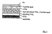
- a solar cell according to the present invention is built of a substrate, followed by a FTO layer, a blocking TiO 2 layer, dye-sensitized TiO 2 with a fluoride layer, hole transport material (HTM), a second fluoride layer, and a gold (Au) layer.
- Figure 3 shows an embodiment of a basic design of an inventive photovoltaic device, comprising a substrate, a TCO-layer, a counter-electrode, especially an Al electrode as well as two fluoride layers, enclosing a blend or bilayer of p- or n-type organic/or polymeric semiconductors.
Landscapes
- Physics & Mathematics (AREA)
- Electromagnetism (AREA)
- Chemical & Material Sciences (AREA)
- Inorganic Chemistry (AREA)
- Hybrid Cells (AREA)
- Photovoltaic Devices (AREA)
- Electroluminescent Light Sources (AREA)
Priority Applications (8)
| Application Number | Priority Date | Filing Date | Title |
|---|---|---|---|
| EP01121178A EP1289028B1 (fr) | 2001-09-04 | 2001-09-04 | Dispositif photovoltaique et procédé de sa fabrication |
| DE60132450T DE60132450T2 (de) | 2001-09-04 | 2001-09-04 | Solarzelle und Herstellungsmethode |
| EP07012986A EP1837930A1 (fr) | 2001-09-04 | 2001-09-04 | Dispositif photovoltaïque et procédé de sa fabrication |
| AU2002300573A AU2002300573B2 (en) | 2001-09-04 | 2002-08-15 | Photovoltaic Device and Method for Preparing the Same |
| US10/234,488 US20030062082A1 (en) | 2001-09-04 | 2002-09-03 | Photovoltaic device and method for preparing the same |
| JP2002259244A JP4023596B2 (ja) | 2001-09-04 | 2002-09-04 | 光起電力装置及びその製造方法 |
| KR1020020053257A KR20030020854A (ko) | 2001-09-04 | 2002-09-04 | 광전 장치 및 이의 제조방법 |
| US11/211,358 US8003884B2 (en) | 2001-09-04 | 2005-08-24 | Photovoltaic device and method for preparing the same |
Applications Claiming Priority (1)
| Application Number | Priority Date | Filing Date | Title |
|---|---|---|---|
| EP01121178A EP1289028B1 (fr) | 2001-09-04 | 2001-09-04 | Dispositif photovoltaique et procédé de sa fabrication |
Related Child Applications (1)
| Application Number | Title | Priority Date | Filing Date |
|---|---|---|---|
| EP07012986A Division EP1837930A1 (fr) | 2001-09-04 | 2001-09-04 | Dispositif photovoltaïque et procédé de sa fabrication |
Publications (2)
| Publication Number | Publication Date |
|---|---|
| EP1289028A1 true EP1289028A1 (fr) | 2003-03-05 |
| EP1289028B1 EP1289028B1 (fr) | 2008-01-16 |
Family
ID=8178540
Family Applications (2)
| Application Number | Title | Priority Date | Filing Date |
|---|---|---|---|
| EP07012986A Ceased EP1837930A1 (fr) | 2001-09-04 | 2001-09-04 | Dispositif photovoltaïque et procédé de sa fabrication |
| EP01121178A Expired - Lifetime EP1289028B1 (fr) | 2001-09-04 | 2001-09-04 | Dispositif photovoltaique et procédé de sa fabrication |
Family Applications Before (1)
| Application Number | Title | Priority Date | Filing Date |
|---|---|---|---|
| EP07012986A Ceased EP1837930A1 (fr) | 2001-09-04 | 2001-09-04 | Dispositif photovoltaïque et procédé de sa fabrication |
Country Status (6)
| Country | Link |
|---|---|
| US (2) | US20030062082A1 (fr) |
| EP (2) | EP1837930A1 (fr) |
| JP (1) | JP4023596B2 (fr) |
| KR (1) | KR20030020854A (fr) |
| AU (1) | AU2002300573B2 (fr) |
| DE (1) | DE60132450T2 (fr) |
Cited By (17)
| Publication number | Priority date | Publication date | Assignee | Title |
|---|---|---|---|---|
| EP1523019A3 (fr) * | 2003-09-26 | 2005-04-20 | Samsung SDI Co., Ltd. | Cellule solaire sensibilisée comportant une couche tampon |
| WO2005060008A1 (fr) * | 2003-12-18 | 2005-06-30 | Dyesol Ltd | Procede d'elaboration par voie electrolytique de couches nanoparticulaires |
| WO2005096403A3 (fr) * | 2004-03-31 | 2006-03-02 | Matsushita Electric Industrial Co Ltd | Élément de conversion photoélectrique organique et sa méthode de production, photodiode organique et capteur d’images l’utilisant, diode organique et sa méthode de production |
| US7180110B2 (en) | 2003-07-08 | 2007-02-20 | Matsushita Electric Industrial Co., Ltd. | Organic photoelectric conversion element |
| AU2004298829B2 (en) * | 2003-12-18 | 2009-01-22 | Dyesol Ltd | Method for electrolytic engineering of nano-particulate layers |
| WO2009034331A1 (fr) * | 2007-09-14 | 2009-03-19 | Molecular Vision Limited | Dispositif photovoltaïque comportant une couche intermédiaire non conductrice |
| WO2010125403A1 (fr) * | 2009-04-30 | 2010-11-04 | Cambridge Enterprise Limited | Dispositifs photovoltaïques contenant des paires d'ions |
| WO2011036145A1 (fr) | 2009-09-24 | 2011-03-31 | Empa | Cellule solaire multicouche composée de couches minces organiques |
| CN102089927A (zh) * | 2008-05-12 | 2011-06-08 | 柯尼卡美能达商用科技株式会社 | 色素增感型太阳能电池及其制造方法 |
| WO2012087930A3 (fr) * | 2010-12-20 | 2012-10-04 | E. I. Du Pont De Nemours And Company | Matériaux électro-actifs |
| EP1351324B1 (fr) * | 2002-04-04 | 2012-12-12 | Samsung Display Co., Ltd. | Dispositif organique électroluminescent comportant carboxylate métallique |
| CN109166732A (zh) * | 2018-09-05 | 2019-01-08 | 陕西理工大学 | 一种Zn掺杂TiO2纳米晶光阳极的制备方法 |
| CN109776395A (zh) * | 2019-03-20 | 2019-05-21 | 北京燕化集联光电技术有限公司 | 一种含氟螺二芴结构的空穴材料及其制备方法与应用 |
| CN109776397A (zh) * | 2019-03-20 | 2019-05-21 | 北京燕化集联光电技术有限公司 | 一种具有9,9′-螺二芴结构的有机化合物及其制备方法与应用 |
| CN109786423A (zh) * | 2019-01-09 | 2019-05-21 | 蜂巢能源科技有限公司 | 钙钛矿/硅叠层太阳能电池及其制备方法和应用 |
| CN113277972A (zh) * | 2021-03-12 | 2021-08-20 | 云南大学 | 基于二苯胺取代咔唑芴杂化的空穴传输材料合成及其在钙钛矿太阳能电池中的应用 |
| CN114181127A (zh) * | 2021-11-12 | 2022-03-15 | 清华大学 | 含硫芴类二苯胺、巯基芴芳胺及其制备方法和应用 |
Families Citing this family (44)
| Publication number | Priority date | Publication date | Assignee | Title |
|---|---|---|---|---|
| AT410729B (de) | 2000-04-27 | 2003-07-25 | Qsel Quantum Solar Energy Linz | Photovoltaische zelle mit einer photoaktiven schicht aus zwei molekularen organischen komponenten |
| AT410859B (de) * | 2000-04-27 | 2003-08-25 | Qsel Quantum Solar Energy Linz | Verfahren zum herstellen einer photovoltaischen zelle mit einer photoaktiven schicht aus zwei organischen komponenten |
| AT411306B (de) * | 2000-04-27 | 2003-11-25 | Qsel Quantum Solar Energy Linz | Photovoltaische zelle mit einer photoaktiven schicht aus zwei molekularen organischen komponenten |
| DE60033038T2 (de) * | 2000-11-24 | 2007-08-23 | Sony Deutschland Gmbh | Hybridsolarzelle mit thermisch abgeschiedener Halbleiteroxidschicht |
| US20060008580A1 (en) * | 2000-11-24 | 2006-01-12 | Gabrielle Nelles | Hybrid solar cells with thermal deposited semiconductive oxide layer |
| JP4461656B2 (ja) * | 2000-12-07 | 2010-05-12 | セイコーエプソン株式会社 | 光電変換素子 |
| DE10326546A1 (de) * | 2003-06-12 | 2005-01-05 | Siemens Ag | Organische Solarzelle mit einer Zwischenschicht mit asymmetrischen Transporteigenschaften |
| JP2005032852A (ja) * | 2003-07-09 | 2005-02-03 | Matsushita Electric Ind Co Ltd | 有機光電変換素子 |
| EP1507298A1 (fr) * | 2003-08-14 | 2005-02-16 | Sony International (Europe) GmbH | Cellule solaire basée sur des nanotubes de carbon |
| GB0319799D0 (en) * | 2003-08-22 | 2003-09-24 | Itm Power Ltd | Photovoltaic cell |
| EP1513171A1 (fr) * | 2003-09-05 | 2005-03-09 | Sony International (Europe) GmbH | Cellule solaire sensibilisé par un colorant et méthode pour sa fabrication |
| KR101065308B1 (ko) * | 2004-02-04 | 2011-09-16 | 삼성에스디아이 주식회사 | 광전기화학전지 |
| KR101042959B1 (ko) * | 2004-06-03 | 2011-06-20 | 삼성에스디아이 주식회사 | 태양전지 및 그 제조방법 |
| KR100644882B1 (ko) * | 2004-07-12 | 2006-11-15 | 한국에너지기술연구원 | 반도체 나노입자를 포함하는 광소자 및 그 제조방법 |
| DE102004040546B3 (de) * | 2004-08-18 | 2006-05-18 | Hahn-Meitner-Institut Berlin Gmbh | Verfahren zum Aufbringen einer Zinksulfid-Pufferschicht auf ein Halbleitersubstrat mittels chemischer Badabscheidung, insbesondere auf die Absorberschicht einer Chalkopyrit-Dünnschicht-Solarzelle |
| KR101137367B1 (ko) * | 2005-01-20 | 2012-04-20 | 삼성전자주식회사 | 표면이 개질된 반도체 전극, 염료 감응 광 전지, 태양전지 및 그 제조 방법, 제조에 사용되는 고분자 조성물 |
| WO2006093109A1 (fr) * | 2005-03-03 | 2006-09-08 | National University Corporation Kyushu Institute Of Technology | Convertisseur photoelectrique et procede pour le fabriquer |
| JP4855146B2 (ja) * | 2005-05-31 | 2012-01-18 | 株式会社リコー | 色素増感太陽電池及び色素増感太陽電池の製造方法 |
| EP1933343A1 (fr) * | 2006-12-13 | 2008-06-18 | Sony Deutschland Gmbh | Méthode de production d'un film semiconductor poreux sur un substrat |
| KR101472308B1 (ko) * | 2007-02-21 | 2014-12-15 | 주식회사 동진쎄미켐 | 신규한 루테늄계 염료 및 이의 제조방법 |
| CN101772858B (zh) * | 2007-08-06 | 2013-10-09 | 东洋制罐株式会社 | 染料敏化型太阳能电池 |
| CN102027556B (zh) * | 2008-04-18 | 2013-04-17 | Nlab太阳能股份公司 | 太阳能向电能转化的装置 |
| WO2010009234A1 (fr) | 2008-07-16 | 2010-01-21 | Wisconsin Alumni Research Foundation | Substrats métalliques comprenant des films minces nanoporeux d'oxyde de métal et leurs procédés de fabrication |
| JP2010034465A (ja) * | 2008-07-31 | 2010-02-12 | Sumitomo Chemical Co Ltd | 光電変換素子 |
| CN102265453B (zh) | 2008-10-29 | 2014-10-01 | 富士胶片株式会社 | 色素、使用其的光电转换元件、光电化学电池、及色素的制造方法 |
| KR100928009B1 (ko) * | 2009-05-29 | 2009-11-24 | 주식회사 티지에너지 | 염료감응 태양전지의 중간체 및 그로부터 염료감응 태양전지를 제조하는 방법 |
| CN101958194B (zh) * | 2009-07-20 | 2011-11-16 | 中国科学院化学研究所 | 微流控染料敏化太阳能电池 |
| JP5524557B2 (ja) | 2009-09-28 | 2014-06-18 | 富士フイルム株式会社 | 光電変換素子の製造方法、光電変換素子、および光電気化学電池 |
| JP5620081B2 (ja) | 2009-09-28 | 2014-11-05 | 富士フイルム株式会社 | 光電変換素子の製造方法 |
| KR101146671B1 (ko) * | 2010-03-04 | 2012-05-22 | 삼성에스디아이 주식회사 | 초임계 유체를 사용하여 금속 산화물 입자에 염료를 흡착하는 방법 |
| WO2012057006A1 (fr) * | 2010-10-29 | 2012-05-03 | 株式会社フジクラ | Module de cellules solaires sensibilisées aux colorants |
| KR101135476B1 (ko) * | 2010-11-16 | 2012-04-13 | 삼성에스디아이 주식회사 | 염료 감응 태양 전지 |
| KR101200698B1 (ko) | 2011-01-27 | 2012-11-12 | 한국기술교육대학교 산학협력단 | 염료감응 태양전지의 작업전극 및 그의 제조방법 |
| US8216872B1 (en) * | 2011-02-21 | 2012-07-10 | National Applied Research Laboratories | Method of integrating light-trapping layer to thin-film solar cell |
| JP5678825B2 (ja) * | 2011-07-12 | 2015-03-04 | コニカミノルタ株式会社 | 光電変換素子及び太陽電池 |
| JP6182145B2 (ja) | 2011-09-28 | 2017-08-16 | 住友化学株式会社 | 発光素子用のスピロビフルオレン化合物 |
| GB201208793D0 (en) | 2012-05-18 | 2012-07-04 | Isis Innovation | Optoelectronic device |
| PL2850627T3 (pl) | 2012-05-18 | 2016-10-31 | Urządzenie optoelektroniczne zawierające porowaty materiał rusztowania oraz perowskity | |
| EP2850669B1 (fr) | 2012-05-18 | 2016-02-24 | Isis Innovation Limited | Dispositif photovoltaïque comprenant des pérovskites |
| JP5972811B2 (ja) | 2013-02-22 | 2016-08-17 | 富士フイルム株式会社 | 光電変換素子、光電変換素子の製造方法および色素増感太陽電池 |
| CN106233486B (zh) * | 2014-04-25 | 2019-06-14 | 富士胶片株式会社 | 光电转换元件、使用该光电转换元件的太阳能电池以及光电转换元件的制造方法 |
| CN104779054B (zh) * | 2014-12-31 | 2017-10-20 | 山东玉皇新能源科技有限公司 | 一种染料敏化太阳能电池复合对电极的制备方法 |
| CN113773614B (zh) * | 2020-06-09 | 2024-06-11 | Tcl科技集团股份有限公司 | 复合材料及其制备方法和发光二极管 |
| CN111799381B (zh) * | 2020-09-10 | 2020-11-27 | 江西省科学院能源研究所 | 一种基于含磷空穴掺杂剂的钙钛矿太阳能电池制备方法 |
Family Cites Families (26)
| Publication number | Priority date | Publication date | Assignee | Title |
|---|---|---|---|---|
| FR2228857B1 (fr) * | 1973-05-09 | 1976-06-25 | Kloeckner Werke Ag | |
| JPS5685876A (en) * | 1979-12-14 | 1981-07-13 | Hitachi Ltd | Photoelectric converter |
| US4532372A (en) * | 1983-12-23 | 1985-07-30 | Energy Conversion Devices, Inc. | Barrier layer for photovoltaic devices |
| DE3516117A1 (de) * | 1985-05-04 | 1986-11-06 | Telefunken electronic GmbH, 7100 Heilbronn | Solarzelle |
| US6127692A (en) * | 1989-08-04 | 2000-10-03 | Canon Kabushiki Kaisha | Photoelectric conversion apparatus |
| JP3016896B2 (ja) * | 1991-04-08 | 2000-03-06 | パイオニア株式会社 | 有機エレクトロルミネッセンス素子 |
| FR2684458B1 (fr) * | 1991-11-29 | 1994-10-21 | Corning Inc | Materiau electrolytique sous forme de gel solide pour la modulation de la lumiere et dispositifs electro-optiques utilisant ce materiau. |
| US5652067A (en) * | 1992-09-10 | 1997-07-29 | Toppan Printing Co., Ltd. | Organic electroluminescent device |
| JPH07307483A (ja) | 1994-05-11 | 1995-11-21 | Fuji Xerox Co Ltd | 有機太陽電池 |
| DK0815166T3 (da) * | 1995-03-14 | 2000-10-23 | Du Pont | Fremgangsmåde til fremstilling af polyvinylbutyralark |
| US5776622A (en) * | 1996-07-29 | 1998-07-07 | Eastman Kodak Company | Bilayer eletron-injeting electrode for use in an electroluminescent device |
| US5677572A (en) * | 1996-07-29 | 1997-10-14 | Eastman Kodak Company | Bilayer electrode on a n-type semiconductor |
| US5925897A (en) * | 1997-02-14 | 1999-07-20 | Oberman; David B. | Optoelectronic semiconductor diodes and devices comprising same |
| US6069442A (en) * | 1997-09-18 | 2000-05-30 | Eastman Kodak Company | Organic electroluminescent device with inorganic electron transporting layer |
| DE19814653A1 (de) * | 1998-04-01 | 1999-10-07 | Bayer Ag | Photovoltaik-Module mit Verbundkörpern |
| US6075203A (en) * | 1998-05-18 | 2000-06-13 | E. I. Du Pont Nemours And Company | Photovoltaic cells |
| US6198092B1 (en) * | 1998-08-19 | 2001-03-06 | The Trustees Of Princeton University | Stacked organic photosensitive optoelectronic devices with an electrically parallel configuration |
| JP2000154254A (ja) * | 1998-11-20 | 2000-06-06 | Mitsubishi Paper Mills Ltd | リチウム2次電池用ゲル状電解質 |
| EP1087412B1 (fr) * | 1999-09-24 | 2008-10-01 | Kabushiki Kaisha Toshiba | Composition d'électrolyte, cellule solaire employant cette composition d'électrolyte, et méthode de fabrication de cette cellule solaire |
| JP4477729B2 (ja) | 2000-01-19 | 2010-06-09 | シャープ株式会社 | 光電変換素子及びそれを用いた太陽電池 |
| AT411306B (de) * | 2000-04-27 | 2003-11-25 | Qsel Quantum Solar Energy Linz | Photovoltaische zelle mit einer photoaktiven schicht aus zwei molekularen organischen komponenten |
| EP1160888A1 (fr) * | 2000-05-29 | 2001-12-05 | Sony International (Europe) GmbH | Matériau transportant de trous de charge et son utilisation dans des dipoitifs photoelectriques |
| JP5081345B2 (ja) * | 2000-06-13 | 2012-11-28 | 富士フイルム株式会社 | 光電変換素子の製造方法 |
| DE60033038T2 (de) * | 2000-11-24 | 2007-08-23 | Sony Deutschland Gmbh | Hybridsolarzelle mit thermisch abgeschiedener Halbleiteroxidschicht |
| EP1289030A1 (fr) * | 2001-09-04 | 2003-03-05 | Sony International (Europe) GmbH | Dopage d'un matériau transportant des trous de charge |
| US7291782B2 (en) * | 2002-06-22 | 2007-11-06 | Nanosolar, Inc. | Optoelectronic device and fabrication method |
-
2001
- 2001-09-04 EP EP07012986A patent/EP1837930A1/fr not_active Ceased
- 2001-09-04 DE DE60132450T patent/DE60132450T2/de not_active Expired - Lifetime
- 2001-09-04 EP EP01121178A patent/EP1289028B1/fr not_active Expired - Lifetime
-
2002
- 2002-08-15 AU AU2002300573A patent/AU2002300573B2/en not_active Ceased
- 2002-09-03 US US10/234,488 patent/US20030062082A1/en not_active Abandoned
- 2002-09-04 JP JP2002259244A patent/JP4023596B2/ja not_active Expired - Fee Related
- 2002-09-04 KR KR1020020053257A patent/KR20030020854A/ko not_active Ceased
-
2005
- 2005-08-24 US US11/211,358 patent/US8003884B2/en not_active Expired - Fee Related
Non-Patent Citations (4)
| Title |
|---|
| BACH U ET AL: "CHARACTERIZATION OF HOLE TRANSPORT IN A NEW CLASS OF SPIRO-LINKED OLIGOTRIPHENYLAMINE COMPOUNDS", ADVANCED MATERIALS, VCH VERLAGSGESELLSCHAFT, WEINHEIM, DE, vol. 12, no. 14, 19 July 2000 (2000-07-19), pages 1060 - 1063, XP000959389, ISSN: 0935-9648 * |
| BRABEC C J ET AL: "Interpenetrating Networks of Fullerenes and Conjugated Polymers for Plastic Photovoltaics", PROCEEDINGS OF THE EUROPEAN PHOTOVOLTAIC SOLAR ENERGY CONFERENCE, XX, XX, vol. 1, 1 May 2000 (2000-05-01), pages 39 - 42, XP002175218 * |
| KRUEGER J ET AL: "MODIFICATION OF TIO2 HETEROJUNCTIONS WITH BENZOIC ACID DERIVATIVES IN HYBRID MOLECULAR SOLID-STATE DEVICES", ADVANCED MATERIALS, VCH VERLAGSGESELLSCHAFT, WEINHEIM, DE, vol. 12, no. 6, 16 March 2000 (2000-03-16), pages 447 - 451, XP000923878, ISSN: 0935-9648 * |
| SHAHEEN S E ET AL: "2.5% EFFICIENT ORGANIC PLASTIC SOLAR CELLS", APPLIED PHYSICS LETTERS, AMERICAN INSTITUTE OF PHYSICS. NEW YORK, US, vol. 78, no. 6, 5 February 2001 (2001-02-05), pages 841 - 843, XP001001022, ISSN: 0003-6951 * |
Cited By (25)
| Publication number | Priority date | Publication date | Assignee | Title |
|---|---|---|---|---|
| EP1351324B1 (fr) * | 2002-04-04 | 2012-12-12 | Samsung Display Co., Ltd. | Dispositif organique électroluminescent comportant carboxylate métallique |
| US7180110B2 (en) | 2003-07-08 | 2007-02-20 | Matsushita Electric Industrial Co., Ltd. | Organic photoelectric conversion element |
| EP1523019A3 (fr) * | 2003-09-26 | 2005-04-20 | Samsung SDI Co., Ltd. | Cellule solaire sensibilisée comportant une couche tampon |
| CN100477287C (zh) * | 2003-12-18 | 2009-04-08 | 戴索有限公司 | 用于纳米颗粒层的电解工程的方法 |
| AU2004298829B2 (en) * | 2003-12-18 | 2009-01-22 | Dyesol Ltd | Method for electrolytic engineering of nano-particulate layers |
| US8002960B2 (en) | 2003-12-18 | 2011-08-23 | Dyesol Ltd. | Method for electrolytic engineering of nano-particulate layers |
| WO2005060008A1 (fr) * | 2003-12-18 | 2005-06-30 | Dyesol Ltd | Procede d'elaboration par voie electrolytique de couches nanoparticulaires |
| WO2005096403A3 (fr) * | 2004-03-31 | 2006-03-02 | Matsushita Electric Industrial Co Ltd | Élément de conversion photoélectrique organique et sa méthode de production, photodiode organique et capteur d’images l’utilisant, diode organique et sa méthode de production |
| WO2009034331A1 (fr) * | 2007-09-14 | 2009-03-19 | Molecular Vision Limited | Dispositif photovoltaïque comportant une couche intermédiaire non conductrice |
| CN102089927B (zh) * | 2008-05-12 | 2013-11-27 | 柯尼卡美能达商用科技株式会社 | 色素增感型太阳能电池及其制造方法 |
| CN102089927A (zh) * | 2008-05-12 | 2011-06-08 | 柯尼卡美能达商用科技株式会社 | 色素增感型太阳能电池及其制造方法 |
| EP2276104A4 (fr) * | 2008-05-12 | 2012-02-29 | Konica Minolta Business Tech | Cellule solaire à colorant et son procédé de fabrication |
| WO2010125403A1 (fr) * | 2009-04-30 | 2010-11-04 | Cambridge Enterprise Limited | Dispositifs photovoltaïques contenant des paires d'ions |
| WO2011036145A1 (fr) | 2009-09-24 | 2011-03-31 | Empa | Cellule solaire multicouche composée de couches minces organiques |
| WO2012087930A3 (fr) * | 2010-12-20 | 2012-10-04 | E. I. Du Pont De Nemours And Company | Matériaux électro-actifs |
| US9685613B2 (en) | 2010-12-20 | 2017-06-20 | E I Du Pont De Nemours And Company | Electroactive materials |
| CN109166732A (zh) * | 2018-09-05 | 2019-01-08 | 陕西理工大学 | 一种Zn掺杂TiO2纳米晶光阳极的制备方法 |
| CN109786423A (zh) * | 2019-01-09 | 2019-05-21 | 蜂巢能源科技有限公司 | 钙钛矿/硅叠层太阳能电池及其制备方法和应用 |
| CN109786423B (zh) * | 2019-01-09 | 2021-09-21 | 无锡极电光能科技有限公司 | 钙钛矿/硅叠层太阳能电池及其制备方法和应用 |
| CN109776395A (zh) * | 2019-03-20 | 2019-05-21 | 北京燕化集联光电技术有限公司 | 一种含氟螺二芴结构的空穴材料及其制备方法与应用 |
| CN109776397A (zh) * | 2019-03-20 | 2019-05-21 | 北京燕化集联光电技术有限公司 | 一种具有9,9′-螺二芴结构的有机化合物及其制备方法与应用 |
| CN113277972A (zh) * | 2021-03-12 | 2021-08-20 | 云南大学 | 基于二苯胺取代咔唑芴杂化的空穴传输材料合成及其在钙钛矿太阳能电池中的应用 |
| CN113277972B (zh) * | 2021-03-12 | 2023-06-16 | 云南大学 | 基于二苯胺取代咔唑芴杂化的空穴传输材料合成及其在钙钛矿太阳能电池中的应用 |
| CN114181127A (zh) * | 2021-11-12 | 2022-03-15 | 清华大学 | 含硫芴类二苯胺、巯基芴芳胺及其制备方法和应用 |
| CN114181127B (zh) * | 2021-11-12 | 2024-04-23 | 深圳无限光能技术有限公司 | 含硫芴类二苯胺、巯基芴芳胺及其制备方法和应用 |
Also Published As
| Publication number | Publication date |
|---|---|
| US20030062082A1 (en) | 2003-04-03 |
| JP4023596B2 (ja) | 2007-12-19 |
| DE60132450T2 (de) | 2008-04-17 |
| KR20030020854A (ko) | 2003-03-10 |
| US8003884B2 (en) | 2011-08-23 |
| JP2003179244A (ja) | 2003-06-27 |
| US20070240761A1 (en) | 2007-10-18 |
| DE60132450D1 (de) | 2008-03-06 |
| AU2002300573B2 (en) | 2006-12-14 |
| EP1837930A1 (fr) | 2007-09-26 |
| EP1289028B1 (fr) | 2008-01-16 |
Similar Documents
| Publication | Publication Date | Title |
|---|---|---|
| EP1289028B1 (fr) | Dispositif photovoltaique et procédé de sa fabrication | |
| US7061009B2 (en) | Solid conjugated semiconductor device having an unmodified hole transport material | |
| EP2560212B1 (fr) | Procédé pour fabriquer une pile solaire à hétérojonction minérale/organique nanostructurée | |
| US7087834B2 (en) | Apparatus and method for photovoltaic energy production based on internal charge emission in a solid-state heterostructure | |
| US7943848B2 (en) | Photoelectric conversion element, method of manufacturing the same and solar cell | |
| US20120312375A1 (en) | All-Solid-State Heterojunction Solar Cell | |
| JP2008186752A (ja) | 光電変換素子及び太陽電池 | |
| US8039741B2 (en) | Photoelectric conversion element and solar cell | |
| KR102167415B1 (ko) | 금속칼코지나이드 화합물로 개질된 n형 반도체를 갖는 태양전지의 제조방법 및 이로 부터 수득되는 태양전지 | |
| KR101551074B1 (ko) | 피리딘계 첨가제가 함유된 장기안정성 고체상 염료감응 태양전지 | |
| JP2009205890A (ja) | 光電変換素子及び太陽電池 | |
| JP5332114B2 (ja) | 光電変換素子及び太陽電池 | |
| EP2538452A2 (fr) | Pile solaire à hétérojonction entièrement en semi-conducteurs | |
| JP2010282780A (ja) | 光電変換素子及び太陽電池 | |
| JP2010009830A (ja) | 光電変換素子及びその製造方法、太陽電池 | |
| JP5605123B2 (ja) | 光電変換素子及び太陽電池 | |
| BENSON-SMITH et al. | Organic donor–acceptor heterojunction solar cells | |
| Grätzel | Solar cells based on sol-gel films | |
| JP2011086481A (ja) | 光電変換素子及び太陽電池 | |
| JP2009218093A (ja) | 光電変換素子及び太陽電池 | |
| KR20170047673A (ko) | 알킬렌디암모늄을 가지는 화합물을 흡수체로 포함하는 태양 전지 | |
| JP2008243668A (ja) | 光電変換素子及び太陽電池 |
Legal Events
| Date | Code | Title | Description |
|---|---|---|---|
| PUAI | Public reference made under article 153(3) epc to a published international application that has entered the european phase |
Free format text: ORIGINAL CODE: 0009012 |
|
| AK | Designated contracting states |
Kind code of ref document: A1 Designated state(s): AT BE CH CY DE DK ES FI FR GB GR IE IT LI LU MC NL PT SE TR |
|
| AX | Request for extension of the european patent |
Extension state: AL LT LV MK RO SI |
|
| 17P | Request for examination filed |
Effective date: 20030327 |
|
| AKX | Designation fees paid |
Designated state(s): DE FR GB NL |
|
| RAP1 | Party data changed (applicant data changed or rights of an application transferred) |
Owner name: SONY DEUTSCHLAND GMBH |
|
| 17Q | First examination report despatched |
Effective date: 20051024 |
|
| RAP1 | Party data changed (applicant data changed or rights of an application transferred) |
Owner name: SONY DEUTSCHLAND GMBH |
|
| GRAP | Despatch of communication of intention to grant a patent |
Free format text: ORIGINAL CODE: EPIDOSNIGR1 |
|
| RIC1 | Information provided on ipc code assigned before grant |
Ipc: H01L 51/42 20060101AFI20070717BHEP |
|
| RIN1 | Information on inventor provided before grant (corrected) |
Inventor name: MITEVA, TZENKA,SONY INTERNATIONAL (EUROPE) GMBH Inventor name: NELLES, GABRIELLE,SONY INTERNATIONAL (EUROPE) GMBH Inventor name: YASUDA, AKIO,SONY INTERNATIONAL (EUROPE) GMBH |
|
| GRAS | Grant fee paid |
Free format text: ORIGINAL CODE: EPIDOSNIGR3 |
|
| GRAA | (expected) grant |
Free format text: ORIGINAL CODE: 0009210 |
|
| AK | Designated contracting states |
Kind code of ref document: B1 Designated state(s): DE FR GB NL |
|
| REG | Reference to a national code |
Ref country code: GB Ref legal event code: FG4D |
|
| REF | Corresponds to: |
Ref document number: 60132450 Country of ref document: DE Date of ref document: 20080306 Kind code of ref document: P |
|
| ET | Fr: translation filed | ||
| PLBE | No opposition filed within time limit |
Free format text: ORIGINAL CODE: 0009261 |
|
| STAA | Information on the status of an ep patent application or granted ep patent |
Free format text: STATUS: NO OPPOSITION FILED WITHIN TIME LIMIT |
|
| 26N | No opposition filed |
Effective date: 20081017 |
|
| PGFP | Annual fee paid to national office [announced via postgrant information from national office to epo] |
Ref country code: GB Payment date: 20120920 Year of fee payment: 12 |
|
| PGFP | Annual fee paid to national office [announced via postgrant information from national office to epo] |
Ref country code: DE Payment date: 20120921 Year of fee payment: 12 |
|
| PGFP | Annual fee paid to national office [announced via postgrant information from national office to epo] |
Ref country code: FR Payment date: 20121010 Year of fee payment: 12 Ref country code: NL Payment date: 20120920 Year of fee payment: 12 |
|
| REG | Reference to a national code |
Ref country code: NL Ref legal event code: V1 Effective date: 20140401 |
|
| GBPC | Gb: european patent ceased through non-payment of renewal fee |
Effective date: 20130904 |
|
| REG | Reference to a national code |
Ref country code: DE Ref legal event code: R119 Ref document number: 60132450 Country of ref document: DE Effective date: 20140401 |
|
| REG | Reference to a national code |
Ref country code: FR Ref legal event code: ST Effective date: 20140530 |
|
| PG25 | Lapsed in a contracting state [announced via postgrant information from national office to epo] |
Ref country code: GB Free format text: LAPSE BECAUSE OF NON-PAYMENT OF DUE FEES Effective date: 20130904 |
|
| PG25 | Lapsed in a contracting state [announced via postgrant information from national office to epo] |
Ref country code: NL Free format text: LAPSE BECAUSE OF NON-PAYMENT OF DUE FEES Effective date: 20140401 Ref country code: FR Free format text: LAPSE BECAUSE OF NON-PAYMENT OF DUE FEES Effective date: 20130930 Ref country code: DE Free format text: LAPSE BECAUSE OF NON-PAYMENT OF DUE FEES Effective date: 20140401 |