EP1291900B1 - Vorrichtung zum Nachweis einer Feinstruktur an der Oberfläche einer Probe und Verfahren zur Herstellung einer Halbleitervorrichtung - Google Patents
Vorrichtung zum Nachweis einer Feinstruktur an der Oberfläche einer Probe und Verfahren zur Herstellung einer Halbleitervorrichtung Download PDFInfo
- Publication number
- EP1291900B1 EP1291900B1 EP02020243A EP02020243A EP1291900B1 EP 1291900 B1 EP1291900 B1 EP 1291900B1 EP 02020243 A EP02020243 A EP 02020243A EP 02020243 A EP02020243 A EP 02020243A EP 1291900 B1 EP1291900 B1 EP 1291900B1
- Authority
- EP
- European Patent Office
- Prior art keywords
- sensor
- sample
- detecting apparatus
- electron
- electron beam
- Prior art date
- Legal status (The legal status is an assumption and is not a legal conclusion. Google has not performed a legal analysis and makes no representation as to the accuracy of the status listed.)
- Expired - Lifetime
Links
Images




Classifications
-
- H—ELECTRICITY
- H01—ELECTRIC ELEMENTS
- H01J—ELECTRIC DISCHARGE TUBES OR DISCHARGE LAMPS
- H01J37/00—Discharge tubes with provision for introducing objects or material to be exposed to the discharge, e.g. for the purpose of examination or processing thereof
- H01J37/02—Details
- H01J37/244—Detectors; Associated components or circuits therefor
-
- H—ELECTRICITY
- H10—SEMICONDUCTOR DEVICES; ELECTRIC SOLID-STATE DEVICES NOT OTHERWISE PROVIDED FOR
- H10P—GENERIC PROCESSES OR APPARATUS FOR THE MANUFACTURE OR TREATMENT OF DEVICES COVERED BY CLASS H10
- H10P74/00—Testing or measuring during manufacture or treatment of wafers, substrates or devices
-
- G—PHYSICS
- G01—MEASURING; TESTING
- G01N—INVESTIGATING OR ANALYSING MATERIALS BY DETERMINING THEIR CHEMICAL OR PHYSICAL PROPERTIES
- G01N21/00—Investigating or analysing materials by the use of optical means, i.e. using sub-millimetre waves, infrared, visible or ultraviolet light
- G01N21/84—Systems specially adapted for particular applications
- G01N21/88—Investigating the presence of flaws or contamination
- G01N21/95—Investigating the presence of flaws or contamination characterised by the material or shape of the object to be examined
- G01N21/9501—Semiconductor wafers
-
- G—PHYSICS
- G03—PHOTOGRAPHY; CINEMATOGRAPHY; ANALOGOUS TECHNIQUES USING WAVES OTHER THAN OPTICAL WAVES; ELECTROGRAPHY; HOLOGRAPHY
- G03F—PHOTOMECHANICAL PRODUCTION OF TEXTURED OR PATTERNED SURFACES, e.g. FOR PRINTING, FOR PROCESSING OF SEMICONDUCTOR DEVICES; MATERIALS THEREFOR; ORIGINALS THEREFOR; APPARATUS SPECIALLY ADAPTED THEREFOR
- G03F1/00—Originals for photomechanical production of textured or patterned surfaces, e.g., masks, photo-masks, reticles; Mask blanks or pellicles therefor; Containers specially adapted therefor; Preparation thereof
- G03F1/68—Preparation processes not covered by groups G03F1/20 - G03F1/50
- G03F1/82—Auxiliary processes, e.g. cleaning or inspecting
- G03F1/84—Inspecting
-
- H—ELECTRICITY
- H01—ELECTRIC ELEMENTS
- H01J—ELECTRIC DISCHARGE TUBES OR DISCHARGE LAMPS
- H01J37/00—Discharge tubes with provision for introducing objects or material to be exposed to the discharge, e.g. for the purpose of examination or processing thereof
- H01J37/26—Electron or ion microscopes; Electron or ion diffraction tubes
- H01J37/285—Emission microscopes, e.g. field-emission microscopes
-
- H—ELECTRICITY
- H01—ELECTRIC ELEMENTS
- H01J—ELECTRIC DISCHARGE TUBES OR DISCHARGE LAMPS
- H01J2237/00—Discharge tubes exposing object to beam, e.g. for analysis treatment, etching, imaging
- H01J2237/244—Detection characterized by the detecting means
- H01J2237/2441—Semiconductor detectors, e.g. diodes
-
- H—ELECTRICITY
- H01—ELECTRIC ELEMENTS
- H01J—ELECTRIC DISCHARGE TUBES OR DISCHARGE LAMPS
- H01J2237/00—Discharge tubes exposing object to beam, e.g. for analysis treatment, etching, imaging
- H01J2237/244—Detection characterized by the detecting means
- H01J2237/2446—Position sensitive detectors
Definitions
- the present invention relates to a detecting apparatus for detecting a fine geometry (an image) on a surface of a sample by irradiating an irradiation beam against the sample and then detecting and processing a secondary radiation emanated from the sample.
- the fine geometry on the surface of the sample includes a defect in such a high density pattern having a minimum line width of 0.15 ⁇ m or smaller formed on a wafer surface of a semiconductor device, for example.
- the present invention also relates to a manufacturing method of a semiconductor device employing such a detecting apparatus.
- a detecting apparatus which comprises an electron gun for emitting an electron beam into a vacuum chamber, an illuminating optical system consisting of a series of electrostatic lenses, a stage for carrying a wafer to be inspected, a map projecting optical system consisting of a series of electrostatic lenses, and a sensor.
- This known detecting apparatus further comprises an MCP (Micro Channel Plate) for amplifying detected electrons, a fluorescent screen for converting the amplified electrons into a light, an FOP (Fiber Optic Plate) functioning as a relay between a vacuum system within a vacuum chamber and an external component for transmitting the optical image converted by the fluorescent screen, and an image-taking device such as a CCD (Charge Coupled Device) for capturing an optical image output from the FOP, wherein the vacuum system within the vacuum chamber is hermetically sealed against an external environment but an electric signal can be transmitted from the inside of the vacuum chamber to the outside thereof.
- MCP Micro Channel Plate
- FOP Field Optic Plate
- CCD Charge Coupled Device
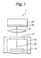
- FIG. 1 and Fig. 2 show schematic diagrams illustrating prior art detecting apparatuses.
- a detecting apparatus of Fig. 1 comprises a vacuum vessel 20 for accommodating a sample 10, or a semiconductor wafer, for example, a hermetic glass plate 21 transparent to the light emitted from the sample, a lens 31 disposed in the atmosphere, a sensor 32, and a camera 33.
- An image signal for the sample generated in the sensor 32 is input to the camera 33 and converted into image data.
- the image data is used in a defect inspection for the sample by a comparative method among dies, that is, a method in which the comparison is applied among pattern images obtained from the corresponding regions (observational screens) of the dies (chips) aligned on different wafers (see JP-A-5-258703 , JP-A-6-188294 ).
- a detecting apparatus 2 shown in Fig. 2 is similar to the detecting apparatus of Fig. 1 with the exception that a sample 10 of Fig. 2 emanates secondary electrons 11, which in turn are converted into a light by a fluorescent screen 19.
- the secondary electrons 11 emanated from the sample 10 by irradiating a primary electron beam against the sample 10 are introduced into the fluorescent screen 19 via an electronic optical system having a lens 12 and an amplifier 13, and then the electrons 11 are converted into the light by the fluorescent screen 19.
- the light from the fluorescent screen 19 is guided out of a vacuum vessel 20 through a hermetic glass plate 21 and passes through a lens 31 to be introduced into a sensor 32.
- the sensor 32 generates an image signal for the sample, which in turn, is input to the camera 33 to be converted into image data.
- the prior art detecting apparatus shown in Fig. 1 and Fig. 2 has such a drawback that the intensity of the light reaching the sensor has been attenuated since in this apparatus the light beam passes through the hermetic glass plate defining the inside and outside of the vacuum vessel and also through the lens and then enters the sensor in the atmosphere so as to be converted into the image signals for the sample surface.
- the attenuation factor of this configuration is observed to be, for example, in the range of 1/20 to 1/2.
- the prior art detecting apparatus also has another problem that the hermetic glass plate and/or the lens may cause an aberration or distortion in the light beam, inhibiting the capturing of highly accurate image.
- the prior art apparatus still has another problem that use of many optical components and supporting and/or fixing parts thereof in the apparatus might sometimes cause a mechanical offset among the sensor, the hermetic glass and the lens, which also inhibit the capturing of highly accurate image.
- the apparatus shown in Fig. 2 using the conventional electron optical system in which the image information represented by the electrons is converted into light and then thus converted light is in turn detected, is also problematic in that the efficiency and resolution may deteriorate as a result of this conversion.
- US-B1-6,184,526 concerns an apparatus and a method for observing and inspecting a predetermined area in a surface of a sample by use of an electron beam.
- the apparatus comprises an MCP for multiplying a secondary beam emerging from the surface of the sample.
- the apparatus and method employ a CCD TDI array in order to increase the lifetime of the MCP, and special scan control is carried out in the observation and inspection operation.
- the apparatus has various structures for enabling correction for positional deviation of the sample and high-speed processing.
- US-B1-6,184,526 describes a detecting apparatus for detecting a fine geometry on a surface of a sample comprising: means for irradiating an irradiation beam against the sample, a sensor, and means for guiding a second radiation emanated from the sample to the sensor. Electrons emanated from the sample are converted to photons by the fluorescent screen and the photons are impinged on a TDI camera which is not in a vacuum environment.
- O.L. KRIVANEK AND P.E. MOONEY "Applications of slow scan CCD cameras in transmission electron microscopy "ULTRAMICROSCOPY, vol. 49, 1993, pages 95-108 , XP009027969 North Holland, discloses that electrons are detected by a CCD through YAG and F/O in a transmission electron microscopy (TEM).
- YAG stands for yttrium-aluminum garnet single-crystal scintillator and is a kind of scintillator. The electrons are converted into a light by the YAG and the light is received by the CCD and the electrons are detected indirectly
- MIROSLAV HOR ⁇ CEK "Detection of the Angular Distribution of the Signal Electrons in VLESEM” JOURNAL OF COMPUTER ASSISTED MICROSCOPY, vol. 10, no. 1, pages 23-32 , discloses an arrangement for very low energy scanning electron microscopy (VLESEM), comprising an immersion objective, a Wien separator and an electron bombarded charge-coupled device (CCD) detector.
- VLESEM very low energy scanning electron microscopy
- the primary electron beam from the source of electrons passes through the Wien filters, which are balanced so that the axial ray with the nominal energy is not affected.
- the primary beam passes through the deflection system, is focused by the magnetic lens, decelerated to the desired energy by the cathode lens, and scanned over the specimen.
- the transport optics directs the signal beam to a suitable detector.
- the focused primary beam probe is scanned by the deflection system over the specimen in the scanning matrix.
- An object of the present invention is to provide a detecting apparatus which provides a solution to the problems pertaining to the apparatuses according to the prior art.
- the object of the present invention is to improve a resolution and a throughput of inspection of a detecting apparatus for detecting a fine geometry (an image) on a surface of a sample by, in an environment different from that of the atmosphere, irradiating an irradiation beam against the sample and then detecting and processing a secondary radiation emanated from the sample.
- a detecting apparatus for detecting a fine geometry on a surface of a sample is provided as set forth in claim 1.
- a sensor package which is constituted so as to include the sensor and the transmission means.
- the wires or pins of the sensor package in the inside of the different environment are connected to connecting sockets of pins of the processing device through pins of a feed through formed in the flange structure.
- a feed through has generally a structure wherein conductive pins penetrate a plate member made of a insulating material, and has an ability to transmit different signals by including a plurality of pins.
- a feed through also has a seal property and can be used at a place to separate the inside from the outside of a different environment.
- the feed through is connected to a place of a flange structure by welding or by using an O-ring.
- the way for attaching a feed through to a vacuum vessel is not limited to a flange structure shown in Fig. 4 but is able to include a fitting-in structure shown in Fig. 3 .
- the irradiation beam is a beam selected from a group consisting of an electron beam, an X-ray, an X-ray laser, an ultraviolet ray and an ultraviolet-ray laser.
- the secondary radiation beam is one selected from a group consisting of secondary electrons, back scattered electrons, reflected electrons, photoelectrons and scattered lights (reflected lights).
- a pressure and a gas species inside of the different environment may be different from those of the outside thereof, which means that, for example, the inside of the different environment is defined as a vacuum and the outside of the different environment is defined as an atmosphere.
- the afore-mentioned one can be used.
- a sensor package which integrates a sensor and signal transmission pins can be used.
- the sensor package has a function of a table for securing and wiring of the sensor. Wirings may be formed between a pad electrode on the surface of the sensor and a pad of the package by using bonder or the like.
- the wiring distance is reduced, and it is possible to improve transmission signal frequency property (e.g. by 20-30%) and to decrease noise (e.g. by 20-30%) of signals.
- a detecting apparatus for detecting a surface geometry of a wafer comprises an electron beam irradiation means for irradiating an electron beam against the wafer, a sensor for detecting secondary radiation beam emanated from the wafer and then outputting a detection signal containing information of the wafer surface, an electronic control means for directing the secondary radiation beam emanating from the wafer onto the sensor, a processing device for processing the detection signal output from the sensor, a vacuum chamber for accommodating the wafer and the sensor, and a transmission means for transmitting the detection signal from the sensor to the processing device.
- the transmission means extends through the flange structure separating the inside of the different environment from the outside thereof.
- the electronic control means may include a mapping optical system comprising, for example, a noise-cut aperture (an aperture provided to cut electrons or a light which could be a noise factor such as stray electrons) and an electronic amplifier.
- a detecting apparatus of the present invention comprises within a vacuum chamber, a mechanism for irradiating the secondary electrons or a reflected light emitted from the wafer, against the sensor, thereby eliminating the need for the optical lens, the FOP, the hermetic glass plate or fittings for them, so that advantageously, the number of components included in the detecting apparatus can be reduced, the accuracy of position and resolution can be improved, the possible deterioration of optical properties in transmission to the sensor can be dissolved, and the apparatus can be manufactured at a lower cost.
- an entrance plane of the sensor may be coated with an anti-reflection film for preventing reflection of incident electrons.
- a light-accepting element may be treated such that an electron permeable insulation film is disposed on a surface thereof and a conductive anti-reflection film is coated over the insulation film.
- a film made of platinum and/or titanium oxide may be used to form the anti-reflection film.
- the detecting apparatus of the present invention is not limited to the applications in different environments such as the vacuum as stated above, but for image detection, the detecting apparatus may be placed, for example, in other environments containing species of gas different from those in the atmosphere or in the water, so far as the environment allows the light or electrons to be transmitted therein.
- An electron beam, an ultraviolet ray (an ultraviolet light), a far ultraviolet ray (a DUV ray: an ultraviolet ray having a wave length in the vacuum ultraviolet ray region of 200 to 10 nm), or a laser beam may be used as the irradiation beam.
- the electron beam When the electron beam is used, the reflected electrons, the back scattered electrons or the secondary electrons emanated from the sample are used for image detection. Here, the reflected electrons have almost the same energy with the incident electron.
- the ultraviolet ray, the DUV ray or the laser beam the photoelectrons is used for the image detection, in which the scattered light generated upon irradiation of such ray or beam onto the sample surface is detected and thus any defects on the sample surface can be detected.
- the ray or beam may be introduced onto the sample surface or from the sample surface into the sensor in an efficient manner by using a quartz fiber or a hollow fiber.
- any combinations of the electron beam with the ultraviolet ray, the far ultraviolet ray or the laser beam may be used as the irradiation beam to be irradiated against the sample surface.
- the electron beam is solely used for irradiation, in some cases, the potential on the sample surface may be changed due to the charge-up, inhibiting the uniform irradiation of the electron beam, but in contrast, the use of the ray or beam such as the ultraviolet ray, the far ultraviolet ray or the laser beam, which can be irradiated onto the sample surface irrespective of the potential thereon, in combination with the electron beam may help obtain the electrons stably and efficiently from the sample surface, which will be used for image acquisition.
- the present invention further discloses a manufacturing method of a semiconductor device including an inspection process for inspecting a wafer for any defects in the course of processing, using the detecting apparatus as discussed above.
- a detection of an image is accomplished by moving the stage 9 so as to detect a predetermined location on the sample 10, and then executing a detecting operation of the location with an appropriate field of view corresponding to a scaling factor at that place for detection, for example, an area of 200 x 200 ⁇ m by using the scaling factor of 300.
- a series of the above mentioned operations should be carried out repeatedly at high speed.
- An electronic signal generated by the sensor 32 consisting of the CCD disposed in the vacuum vessel 20 is drawn out of the vacuum vessel 20 via a feed through 22 so as to be input to a camera 33. Comparisons among images may be carried out by moving the areas subject to comparison into the place for detection to capture the images thereof repeatedly and applying comparisons among obtained data.
- Fig. 4 is a schematic diagram of a detecting apparatus 4 containing a mapping optical system according to another embodiment of the present invention.
- a sensor 32 is an EB-TDI (Electron Beam detecting Time Delay and Integration) sensor and the sensor 32 allows the electrons to enter the sensor surface directly in a vacuum environment.
- the TDI sensor is representative of such a CCD sensor having a sensor structure and function for achieving a TDI (Time Delay and Integration) driving, which integrates the signals by TDI driving during line scanning thus to enable an image taking in a serial moving mode with a high sensitivity and a high signal volume.
- TDI Time Delay and Integration
- the structure and circuitry of the TDI sensor are widely different from those in the typical CCD so as to enable the TDI driving.
- the TDI sensor can form a two-dimensional image by capturing the optical signals.
- the EB-TDI sensor 32 is referred to as such a TDI sensor that permits the electrons to enter the TDI sensor directly and accumulates and integrates the charges thus to form the two-dimensional image.
- the EB-TDI sensor 32 may be installed in a package, and the package forms a feed through 22. A pin of the package is directly connected to a camera 33 in the atmosphere side.
- An electron optical system 18 may provide the two-dimensional information of a surface of a sample 10 such as a wafer in a scale factor of about 50 to 500 through three-step of lenses 15, 16 and 17. This means that the electron optical system 18 magnifies the electron beam exited from the two-dimensional area and irradiates thus magnified electron beam directly onto the EB-TDI sensor 32.
- the wafer 10 mounted on the stage 9 (movable in the x-, y- and ⁇ - direction, for example) is serially moved in the direction for integration on the sensor surface (the direction indicated by the arrow S in Figs. 11 and 12 ) of the EB-TDI sensor 32, so that the electrons emanated from the wafer surface can enter the EB-TDI sensor 32 through an electron optical system of map projection type and so on.
- the electrons multiplied by the integration steps are made to enter the EB-TDI sensor to form the two-dimensional image.
- the line pixel information from 4000 lines is integrated serially with 500 steps, as the stage 9 moves, so that a sensor charge intensity responsive to each pixel of the sample can be accumulated sufficiently.
- the electron beam or other irradiation beam may be irradiated onto the subject to determine the presence of a defective event such as dusts, a bad conduction, a bad pattern or a lack of pattern, and also to make a state judgment and a sort categorization.
- the detecting apparatus 4 of Fig. 4 can achieve a high resolution, a high processing rate, a lower profile, and at a low cost.
- Fig. 5 is a schematic diagram of a detecting apparatus 5 according to another embodiment of the present invention.
- an ultraviolet ray 43 selected as the primary beam is directed onto a surface of a sample 10, and photoelectrons emanated from the incident points on the surface are guided through a lens, an aperture, a stigmatic element and so on included in an electron optical system 12 so as to enlarge an electron image, which is in turn made to enter a sensor 32.
- the sensor 32 comprises an EB-CCD sensor or an EB-TDI sensor.
- the ultraviolet ray 43 or the primary beam is transmitted through a hollow fiber 44 and irradiated to a field of view surrounding the center axis of the electron optical system, for example, an area defined with a diameter of 300 ⁇ m.
- Fig. 6 is a schematic diagram of a detecting apparatus 6 according to another embodiment of the present invention.
- the detecting apparatus 6 uses a combination of an electron beam 45 and a laser beam 46 as the primary beam.
- a direction of the electron beam 45 is changed by an E x B filter 47 so as to be aligned with an optical axis 49 of an electronic optical system for detection, and then the electron beam 45 enters a sample 10.
- a secondary electron beam 11 emanated from the sample 10 goes straight through the E x B filter 47 and is introduced into a sensor 32.
- the sensor 32 is composed of the EB-TDI sensor.
- the laser beam 46 may be a quadruple wave of the YAG or an excimer laser.
- the excimer laser may be introduced through a hollow fiber.
- Fig. 7 is a schematic diagram of a detecting apparatus 7 according to another embodiment of the present invention.
- the detecting apparatus 7 is an electron beam detecting apparatus of map projection type, in which an electron beam 82 emitted from an electron gun 81 is shaped through a square opening, contracted by a two-step of lenses 83, 84, and focused onto a central area on a deflecting plane of an E x B filter 85, forming a square image having each side of 1.25 mm.
- E x B filter 85 forming a square image having each side of 1.25 mm.
- shaped beam which has been deflected by the E x B filter 85, is then contracted into a scale of 1/5 by lenses 88, 89 and projected on a sample 10.
- Secondary electrons emanated from the sample which contain information of a pattern image, are enlarged through a four-step of lenses 89, 88, 92 and 93, and made to enter a sensor 32.
- the lens 89 in combination with the lens 88 forms a symmetric tablet lens
- the lens 92 in combination with the lens 93 forms another symmetric tablet lens, meaning that the series of lenses 89, 88, 92 and 93 together form a non-distortion lens set.
- a reference pattern should be regularly placed on the surface of the sample to measure any distortions, so that parameters to be used to compensate for the distortions could be calculated beforehand.
- the sample is such a wafer that an oxide film or a nitride film may be selectively formed thereon, only making a correction to the optical distortion is not sufficient, but in this case, another step of correction to the distortion should be added upon acquisition of the image data by selecting representative points from the edge portion of the pattern and comparing those points to the image of the data. Subsequently, a die-to-die comparison, or a comparison between images of the patterns obtained from the same regions (the observational screens) of dies (chips) arranged on different wafers, or another comparison between plural sets of image data may be applied to detect any defects.
- the EB-CCD sensor or the EB-TDI sensor to which the electrons are irradiated directly to make an image detection, is installed in the vacuum environment, the image acquisition can be accomplished with high contrast and high resolution and also a higher throughput without any optical transmission loss can be achieved at a lower cost as compared to the detecting apparatuses according to the prior art.
- the electron beam to be irradiated onto the wafer is prepared so as to have, for example, a beam energy within the range of 10 to 4000eV, and an elliptical beam profile with a radius "a" of 250 ⁇ m and a radius "b" of 100 ⁇ m, and irradiated onto the wafer surface approximately perpendicularly thereto.
- a current density should be set to be within the range of 1 x 10 -5 to 1 x 10 -1 A/cm 2 .
- An amount of emission of the secondary electrons depends on the current density of the irradiated electron beam or the total current value thereof. When an emission ratio of the secondary electrons is 1, the same amount of secondary electrons as that of the incident electrons may be emanated.
- Energy of the secondary electrons is typically within the range of 0 to several eV.
- a scale factor of a sample surface to a sensor surface of the mapping optical system is assumed to be 200, and if the field of view on the wafer (visual field) is 200 ⁇ m x 50 ⁇ m, a corresponding area on the sensor surface should be 40 mm x 10 mm.
- the current value irradiated within the 200 ⁇ m x 50 ⁇ m field of view is 2 ⁇ A and the emission ratio is 1, the amount of emanated secondary electrons is 2 ⁇ A.
- the emanated secondary electrons pass through the objective lenses 88 and 89, and then pass the E x B filter 85 under a rectilinear propagation condition. Subsequently, the beam of the secondary electrons is enlarged by the lens 92, NA aperture (not shown) and the lens 93, and then enters the sensor surface.
- the NA aperture (not shown) functions to limit a transmittance and an aberration.
- a current of 2 ⁇ A x 0.03 60nA enters the sensor surface.
- the EB-TDI sensor or the EB-CCD sensor is used as the sensor.
- 2-dimensional image can be obtained while moving continuously.
- the wafer mounted on the stage movable in x-, y-, ⁇ - and z-directions is continuously moved along a direction corresponding to the integrating direction of the sensor so as to integrate the charges of the EB-TDI sensor and to obtain the image.
- the pixel size is 20 ⁇ m x 20 ⁇ m
- the pixel number is 2000 x 500
- 500 steps of pixels are arranged in the integrating direction.
- the electron beam to be irradiated onto the wafer is prepared so as to have, for example, a beam energy within the range of 10 to 4000eV, and an elliptical beam profile with a radius "a" of 250 ⁇ m and a radius "b" of 100 ⁇ m, and irradiated onto the wafer surface approximately perpendicularly thereto.
- a current density should be set to be within the range of 1 x 10 -3 to 5 x 10 -1 A/cm 2 .
- An amount of emission of the reflected electrons depends on the current density of the irradiated electron beam or the total current value thereof.
- the electrons emanated from the sample surface with the same energy as of the incident electron beam are treated as the reflected electrons.
- the emission ratio of the reflected electrons is lower than that of the secondary electrons and is typically less than 1/10.
- a scale factor of the sample surface to the sensor surface of the mapping optical system is assumed to be 200, and if the field of view on the wafer (visual field) is 200 ⁇ m x 50 ⁇ m, a corresponding area on the sensor surface should be 40 mm x 10 mm.
- the current value irradiated within the 200 ⁇ m x 50 ⁇ m field of view is 2 ⁇ A and the emission ratio is 0.1, the amount of emanated reflected electrons is 0.2 ⁇ A.
- the emanated reflected electrons pass through the objective lenses 88 and 89, and then pass the E x B filter 85 under a rectilinear propagation condition. Subsequently, the beam of the reflected electrons is enlarged by the lens 92, NA aperture (not shown) and the lens 93, and then enters the sensor surface.
- the NA aperture functions to limit a transmittance and an aberration.
- the EB-TDI sensor or the EB-CCD sensor is used as the sensor.
- 2-dimensional image can be obtained while moving continuously.
- the wafer mounted on the stage movable in x, y, ⁇ and z directions is continuously moved along a direction corresponding to the integrating direction of the sensor so as to integrate the charges of the EB-TDI sensor and to obtain the image.
- the pixel size is 20 ⁇ m x 20 ⁇ m
- the pixel number is 2000 x 500
- 500 steps of pixels are arranged in the integrating direction.
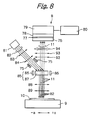
- Fig. 8 is a schematic diagram of an electron beam detecting apparatus 8 of projection type according to another embodiment of the present invention.
- an electron gun 81 emits a plurality of primary electron beams 82.
- respective primary electron beams 82 pass though lenses 83 and 84 and then focused on a central area on a deflecting plane of an E x B deflector 85 (the Wien filter 85) composed of an electrode 86 and a magnet 87, each forming an elliptical image thereon.
- each primary electron beam 82 is, for example, focused on the central area of the deflecting plane of the Wien filter 85 by the two-step of lenses 83 and 84 so as to form the elliptical image of 10 ⁇ m x 12 ⁇ m, and also is operated by a deflector 75 to make a raster-scanning in the direction orthogonal to the drawing paper, so that the primary electron beams, as a whole, can cover uniformly a rectangular area of 1 mm x 0.25 mm (the central area on the deflecting plane of the Wien filter 85).
- the primary electron beam is deflected by the Wien filter 85, demagnified by a lens 88 in a scale, for example, of 1/5, and irradiated generally vertically onto a sample 10 so as to cover a specific area of 200 ⁇ m x 50 ⁇ m on the sample 10.
- the plurality of primary electron beams 82 is scanned by the deflector 75 all at once in the direction orthogonal to the drawing paper, while a stage 9 carrying the sample 10 thereon is serially moved in the +a (or -a) direction, whereby the electron beams, as a whole, are irradiated uniformly on the rectangular area on the surface of the sample 10.
- the stage 9 is moved by steps in the direction of scanning (the direction orthogonal to the drawing paper) by a scanning width of the electron beams 82, and subsequently the stage 9 is serially moved in the -a (or +a) direction opposite to the direction of last movement.
- the sample 10 emanates secondary electrons, back scattered electrons and reflected electrons 11 from respective irradiation points in response to the irradiation of the electron beams.
- the beam of the emanated secondary electrons or reflected electrons 11 are magnified by the lenses 89, 88, 92 and 93, and then a magnetic lens 94 makes the angle correction between the orientation of the light accepting plane of the TDI-CCD sensor 79 and the serial movement direction "a" of the sample 10.
- the beam of the secondary electrons after having experienced the angle correction, is focused on a micro channel plate (MCP) 76 to form a rectangular image as a whole.
- MCP micro channel plate
- These secondary electrons are increased in sensitivity by 10,000 to several 10,000 times by the MCP 76, converted into a light by a scintillator or a fluorescent section 77, and then pass through a relay optical system 78 into the TDI-CCD sensor 79, where the secondary electrons become electric signals in synchronization with the serial movement velocity of the sample and displayed as a series of images on an image display section 80.
- the electron beam needs to be adjusted so as to be irradiated against the surface of the sample 10 as uniformly as possible with reduced uneven irradiation, for example, in a rectangular or elliptical shape of irradiation. Further, in order to improve the throughput, a large amount of irradiation current needs to be applied to the area of detection. This is because applying larger amount of irradiation current allows the moving velocity of the stage to increase correspondingly, thereby improving the throughput.
- the electron beam apparatus of projection type is problematic in that more obstacles are apt to occur in imaging process due to the charge-up resultant from a block irradiation of the electron beam applied against an extended image observation area all at once.
- the unevenness in irradiation can be reduced, for example, to 1/3 as compared to the case of conventional electron beam apparatus.
- the electron beam apparatus may comprise, in addition to the lenses, a variety of apertures, such as numerical apertures (NA) and field apertures, a deflecting systems (aligners) including four or more poles for axial alignment of the electron beam, an stigmatism corrector (a stigmeter), and units required for illuminating and imaging operation for the electron beam including a plurality of quadrupole lenses (four-pole lenses) for modifying the beam shape.
- NA numerical apertures
- field apertures a deflecting systems (aligners) including four or more poles for axial alignment of the electron beam
- an stigmatism corrector a stigmeter
- units required for illuminating and imaging operation for the electron beam including a plurality of quadrupole lenses (four-pole lenses) for modifying the beam shape.
- Fig. 11 is a plan view illustrating pixels P11 to Pij on the sensor surface 91 of the EB-TDI sensor 76.
- the arrow S indicates the direction of integration on the sensor surface 91.
- Fig. 12 is a schematic diagram illustrating a physical relationship between the EB-TDI sensor 76 and a secondary electron beam.
- the arrow S indicates the direction of integration on the sensor surface 91
- the arrow T indicates the direction of the continuous movement of the stage 9 carrying the wafer 10 thereon.
- Fig. 12 if the secondary electron beam 11 from the wafer 10 is being emanated from the same location on the wafer 10 for a certain period of time, as the stage 9 moves in the direction indicated by the arrow S, the secondary electron beam 11 sequentially enters a series of locations a, b, c, d, e,...,i (i represents the number of integration steps) on the optical system 18 of map projection type in order of a ⁇ b ⁇ c ⁇ d ⁇ e . . . ⁇ i.
- the secondary electron beam 11, having once entered the optical system 18 of map projection type, is sequentially emitted from a series of locations a', b', c', d', e', ..., i' on the optical system 18 of map projection type.
- the movement for the charge integration of the EB-TDI sensor 76 in the direction of integration is synchronized with the movement of the stage 9, then the secondary electrons emitted from the locations a', b', c', d', e', ..., i' of the optical system 18 of map projection type sequentially enter the same points on the sensor surface 91, thereby enabling the charges to be integrated by the number of integration steps i.
- respective pixels P11 to Pij on the sensor surface 91 can obtain more signals of the emitted electrons, thereby achieving the higher S/N ratio and allowing to obtain the two-dimensional (electronic) image at higher rate.
- the optical system 18 of map projection type has, for example, a scale factor of 300.
- the information processing section which is not shown, may be arranged after the TDI-CCD sensor 79, so that the information processing section may use the image information obtained in the TDI-CCD sensor 79 to make a comparison among a plurality of cell images and/or a plurality of die images, thereby detecting defects on the surface of the sample and determining the features such as the shape, the position coordinates and the number of the detected defects, which may in turn be indicated on the image display section.
- an adequate condition for irradiation should be individually set for each different sample, and thus obtained images will be indicated on the image display section 80, from which the defects may be detected.
- Fig. 9 is a flow chart illustrating an embodiment of a method of manufacturing a semiconductor device using a electron beam detecting apparatus according to the present invention.
- the manufacturing processes shown in Fig. 9 include the following main processes:
- the respective main processes are further comprised of several sub-processes.
- Right part of Fig. 9 shows sub-processes of the wafer processing process 53.
- the wafer processing process 53 set forth in (3) exerts critical affections to the performance of resulting semiconductor devices 57.
- This process involves sequentially laminating designed circuit patterns on the wafer to form a large number of chips which operate as memories, MPUs and so on.
- the wafer processing process includes the following sub-processes:
- the wafer processing process 53 is repeated a number of times equal to the number of required layers to manufacture semiconductor devices which operate as designed.
- FIG. 9 shows above mentioned processes (6), (9) and (10) together in a block 64, comprising an additional wafer testing process 65.
- Block 66 shows the processes repeated.
- Fig. 10 is a flow chart illustrating the detail of the lithography process 63 in the manufacturing method of Fig. 9 .
- the lithography process 63 includes the following steps:
- the detecting apparatus according to the present invention in which secondary electrons emanated from the wafer are irradiated onto the sensor within the vacuum chamber, no longer requires an optical lens, an FOP, a hermetic glass or fittings for those components, thereby achieving a reduced number of components included in the detecting apparatus, an improved position accuracy and resolution, an elimination of the possible deterioration in the optical features transmitted to the sensor, and a lower cost of the apparatus.
- the present invention can improve the contrast by 2 to 4 times, reduce the cost of the detecting apparatus by 30 to 50%, improve the resolution by 1.5 to 3 times, and reduce the size of the detecting apparatus by about 50%.
- the use of the detecting apparatus according to the present invention can provide an inspection performance to a surface of a sample with a high resolution as well as a high throughput.
Landscapes
- Chemical & Material Sciences (AREA)
- Analytical Chemistry (AREA)
- Physics & Mathematics (AREA)
- General Physics & Mathematics (AREA)
- Biochemistry (AREA)
- Life Sciences & Earth Sciences (AREA)
- Health & Medical Sciences (AREA)
- General Health & Medical Sciences (AREA)
- Immunology (AREA)
- Pathology (AREA)
- Testing Or Measuring Of Semiconductors Or The Like (AREA)
- Analysing Materials By The Use Of Radiation (AREA)
- Length-Measuring Devices Using Wave Or Particle Radiation (AREA)
Claims (11)
- Eine Detektiervorrichtung (3-8) zum Detektieren einer Feingeometrie oder eines Musters auf einer Oberfläche einer Probe (10), wobei Folgendes vorgesehen ist:ein Mittel zur Strahlung eines Bestrahlungsstrahls (43, 45, 46, 82) gegen die Probe, platziert in einer Vakuumumgebung (20), unterschiedlich von einer Atmosphäre;einen EB-TDI-Sensor oder einen EB-CCD-Sensor (32) zum direkten Empfang sekundärer Elektronen, austretend aus der Probe;ein Mittel zur Führung der sekundären Elektronen, ausgetreten bzw. emittiert aus der Probe zu dem Sensor;eine Verarbeitungsvorrichtung (33) zur Verarbeitung einer Detektionssignalausgangsgröße vom Sensor;ein Sendemittel (22) eine Struktur durchdringend, die die Innenseite der Vakuumumgebung (20) von der Außenseite trennt und zwar als eine Hindurchführung um das Detektionssignal von dem Sensor zu der Verarbeitungsvorrichtung zu übertragen oder zu senden, undeine Sensorpackung, die den Sensor (32) und die Sendemittel (22) integriert,wobei der Sensor auf einer Innenseite der Vakuumumgebung (20) angeordnet ist und wobei die Verarbeitungsvorrichtung (33) an einer Außenseite der Vakuumumgebung angeordnet ist.
- Eine Detektiervorrichtung nach Anspruch 1, wobei der Sensor (32) 100 oder mehr Stifte (Pins) besitzt.
- Eine Detektiervorrichtung nach Anspruch 1 oder 2, wobei ferner eine Elektronenquelle (81) und ein elektronen-optischer Steuermechanismus (83, 84) vorgesehen sind, wobei der elektronen-optische Steuermechanismus eine Elektronenstrahl-Ausganggröße von der Elektronenquelle so steuert, um den Elektronenstrahl in die Probe (10) zu leiten.
- Eine Detektiervorrichtung nach Anspruch 3, wobei ferner eine Rausch-Abschneidöffnung vorgesehen ist.
- Eine Detektiervorrichtung nach Anspruch 3 oder 4, wobei der elektronen-optische Steuermechanismus ein optisches Kartensystem (map optical system) aufweist.
- Eine Detektiervorrichtung nach Anspruch 1 oder 2, wobei der Bestrahlungsstrahl ein Strahl ist, der aus einer Gruppe, die Folgendes enthält, ausgewählt ist: einen Röntgenstrahl, einen Ultraviolettstrahl (43) und einen Ultraviolett-Laserstrahl (46).
- Eine Detektiervorrichtung nach Anspruch 1 oder 2, wobei der Bestrahlungsstrahl entweder eine Kombination eines Elektronenstrahls (45) und eines Ultraviolettstrahls (43) ist, oder eine andere Kombination aus einem Elektronenstrahl und einem Röntgenstrahl.
- Eine Detektiervorrichtung nach Anspruch 1 oder 2, wobei der Bestrahlungsstrahl entweder eine Kombination aus einem Elektronenstrahl (45) und einem Ultraviolett-Laserstrahl (46) ist oder eine andere Kombination aus einem Elektronenstrahl und einem Röntgen-Laserstrahl.
- Eine Defektinspektionsvorrichtung mit einer Detektiervorrichtung (3-8) gemäß einem der Ansprüche 1-8.
- Eine Defektinspektionsvorrichtung nach Anspruch 9, wobei ferner Folgendes vorgesehen ist:ein Probentransportmechanismus;eine Probeklemm- oder Haltevorrichtung; undeine Stufe (9) zum Tragen der Probe darauf, wobei all diese Komponenten durch einen Computer gesteuert werden.
- Ein Herstellungsverfahren für eine Halbleitervorrichtung einschließlich eines Verfahrens zum Inspizieren eines Wafers im Hinblick auf irgendwelche Defekte, aufgetreten im Laufe des Erarbeitens, wobei eine Detektiervorrichtung (3-8) oder eine Defektinspektionsvorrichtung, definiert in einem der Ansprüche 1-10 verwendet wird.
Priority Applications (2)
| Application Number | Priority Date | Filing Date | Title |
|---|---|---|---|
| EP10001779.7A EP2190002B8 (de) | 2001-09-10 | 2002-09-10 | Verfahren zur Erfassung einer feinen Geometrie |
| EP16172147.7A EP3089193A1 (de) | 2001-09-10 | 2002-09-10 | Verfahren zur erfassung einer feinen geometrie |
Applications Claiming Priority (2)
| Application Number | Priority Date | Filing Date | Title |
|---|---|---|---|
| JP2001273432 | 2001-09-10 | ||
| JP2001273432 | 2001-09-10 |
Related Child Applications (3)
| Application Number | Title | Priority Date | Filing Date |
|---|---|---|---|
| EP10001779.7A Division EP2190002B8 (de) | 2001-09-10 | 2002-09-10 | Verfahren zur Erfassung einer feinen Geometrie |
| EP16172147.7A Division EP3089193A1 (de) | 2001-09-10 | 2002-09-10 | Verfahren zur erfassung einer feinen geometrie |
| EP10001779.7 Division-Into | 2010-02-22 |
Publications (3)
| Publication Number | Publication Date |
|---|---|
| EP1291900A2 EP1291900A2 (de) | 2003-03-12 |
| EP1291900A3 EP1291900A3 (de) | 2003-05-28 |
| EP1291900B1 true EP1291900B1 (de) | 2011-01-12 |
Family
ID=19098650
Family Applications (3)
| Application Number | Title | Priority Date | Filing Date |
|---|---|---|---|
| EP16172147.7A Withdrawn EP3089193A1 (de) | 2001-09-10 | 2002-09-10 | Verfahren zur erfassung einer feinen geometrie |
| EP10001779.7A Expired - Lifetime EP2190002B8 (de) | 2001-09-10 | 2002-09-10 | Verfahren zur Erfassung einer feinen Geometrie |
| EP02020243A Expired - Lifetime EP1291900B1 (de) | 2001-09-10 | 2002-09-10 | Vorrichtung zum Nachweis einer Feinstruktur an der Oberfläche einer Probe und Verfahren zur Herstellung einer Halbleitervorrichtung |
Family Applications Before (2)
| Application Number | Title | Priority Date | Filing Date |
|---|---|---|---|
| EP16172147.7A Withdrawn EP3089193A1 (de) | 2001-09-10 | 2002-09-10 | Verfahren zur erfassung einer feinen geometrie |
| EP10001779.7A Expired - Lifetime EP2190002B8 (de) | 2001-09-10 | 2002-09-10 | Verfahren zur Erfassung einer feinen Geometrie |
Country Status (7)
| Country | Link |
|---|---|
| US (2) | US7075072B2 (de) |
| EP (3) | EP3089193A1 (de) |
| JP (2) | JP3886871B2 (de) |
| KR (1) | KR100888688B1 (de) |
| CN (2) | CN1310025C (de) |
| DE (1) | DE60238892D1 (de) |
| TW (1) | TW589723B (de) |
Cited By (2)
| Publication number | Priority date | Publication date | Assignee | Title |
|---|---|---|---|---|
| RU2608382C1 (ru) * | 2015-10-15 | 2017-01-18 | Акционерное общество "Лыткаринский завод оптического стекла" | Способ установки ионного источника относительно обрабатываемой детали |
| TWI890306B (zh) * | 2020-12-16 | 2025-07-11 | 荷蘭商Asml荷蘭公司 | 電子束系統及相關之非暫時性電腦可讀媒體 |
Families Citing this family (30)
| Publication number | Priority date | Publication date | Assignee | Title |
|---|---|---|---|---|
| EP1721330A2 (de) * | 2004-03-05 | 2006-11-15 | Oi Corporation | Fokalebenen-detektorbaugruppe eines massenspektrometers |
| US7480082B2 (en) * | 2004-03-31 | 2009-01-20 | Carestream Health, Inc. | Radiation image scanning apparatus and method |
| JP4613554B2 (ja) * | 2004-09-08 | 2011-01-19 | カシオ計算機株式会社 | 電子顕微鏡 |
| TW200629454A (en) | 2005-02-14 | 2006-08-16 | Powerchip Semiconductor Corp | Method of detecting piping defect |
| KR101279028B1 (ko) * | 2005-02-17 | 2013-07-02 | 가부시키가이샤 에바라 세이사꾸쇼 | 전자선장치 |
| DE102005061834B4 (de) | 2005-12-23 | 2007-11-08 | Ioss Intelligente Optische Sensoren & Systeme Gmbh | Vorrichtung und Verfahren zum optischen Prüfen einer Oberfläche |
| JP2007335125A (ja) * | 2006-06-13 | 2007-12-27 | Ebara Corp | 電子線装置 |
| US7544950B2 (en) * | 2006-10-30 | 2009-06-09 | Applied Materials, Israel, Ltd. | Microscope with vacuum objective |
| JP2008233035A (ja) * | 2007-03-23 | 2008-10-02 | Toshiba Corp | 基板検査方法 |
| US8175831B2 (en) | 2007-04-23 | 2012-05-08 | Kla-Tencor Corp. | Methods and systems for creating or performing a dynamic sampling scheme for a process during which measurements are performed on wafers |
| JP4988444B2 (ja) * | 2007-06-19 | 2012-08-01 | 株式会社日立製作所 | 検査方法および装置 |
| NL2003263A (en) * | 2008-08-20 | 2010-03-10 | Asml Holding Nv | Particle detection on an object surface. |
| FR2942070B1 (fr) * | 2009-02-11 | 2011-03-11 | Commissariat Energie Atomique | Procede de correction d'astigmatisme en imagerie par spectromicroscopie a emission d'electrons |
| CN102175933B (zh) * | 2011-01-28 | 2013-09-11 | 南京理工大学 | 微通道板噪声因子测试方法 |
| JP5963453B2 (ja) * | 2011-03-15 | 2016-08-03 | 株式会社荏原製作所 | 検査装置 |
| US9049353B2 (en) | 2011-09-28 | 2015-06-02 | Semiconductor Components Industries, Llc | Time-delay-and-integrate image sensors having variable integration times |
| US10401374B2 (en) * | 2014-11-30 | 2019-09-03 | Tichauer Technical Laboratories, Llc | Device and method of detecting and generating combined modulated particle wave-fronts |
| FR3042615B1 (fr) * | 2015-10-20 | 2017-12-08 | Shyftec | Dispositif pour emettre un signal d'authentification |
| DE112016006424T5 (de) * | 2016-03-16 | 2018-11-15 | Hitachi High-Technologies Corporation | Defektinspektionsverfahren und Defektinspektionsvorrichtung |
| CN108604522B (zh) * | 2016-03-28 | 2020-07-14 | 株式会社日立高新技术 | 带电粒子束装置以及带电粒子束装置的调整方法 |
| US11480606B2 (en) * | 2016-06-14 | 2022-10-25 | Taiwan Semiconductor Manufacturing Co., Ltd. | In-line device electrical property estimating method and test structure of the same |
| CN108646167B (zh) * | 2018-04-27 | 2020-12-04 | 中科晶源微电子技术(北京)有限公司 | 用于半导体器件的激光辅助的电子束检测设备和方法 |
| KR102630568B1 (ko) * | 2018-06-15 | 2024-01-29 | 삼성전자주식회사 | 반도체 소자의 제조 방법 |
| JP7102271B2 (ja) * | 2018-07-17 | 2022-07-19 | ファスフォードテクノロジ株式会社 | 半導体製造装置および半導体装置の製造方法 |
| US10753729B2 (en) | 2018-10-02 | 2020-08-25 | Saudi Arabian Oil Company | Photonic sensing analytical device |
| JP7157708B2 (ja) * | 2019-06-25 | 2022-10-20 | 株式会社荏原製作所 | 電子線検査装置の二次光学系を評価する方法 |
| US11079671B2 (en) | 2019-08-23 | 2021-08-03 | Taiwan Semiconductor Manufacturing Company Ltd. | Fabricating method of photomask, photomask structure thereof, and semiconductor manufacturing method using the same |
| US12416589B2 (en) | 2022-06-24 | 2025-09-16 | SanDisk Technologies, Inc. | Systems and methods for non-destructive inspection of semiconductor devices using reflective X-ray microscope tomographic imaging |
| US20250166963A1 (en) * | 2023-11-21 | 2025-05-22 | Fei Company | Method and System for Imaging a Sample |
| CN120253898A (zh) * | 2025-06-09 | 2025-07-04 | 凯明(常州)新材料科技有限公司 | 一种钢丝表面缺陷的检测方法 |
Family Cites Families (37)
| Publication number | Priority date | Publication date | Assignee | Title |
|---|---|---|---|---|
| US4453086A (en) * | 1981-12-31 | 1984-06-05 | International Business Machines Corporation | Electron beam system with reduced charge buildup |
| KR860002082B1 (ko) * | 1983-01-19 | 1986-11-24 | 가부시기가이샤 도시바 | 레지스트 패턴의 형성 방법 및 장치 |
| US4666228A (en) * | 1983-09-28 | 1987-05-19 | Pave Technology Co. | Hermetic connector and method |
| US4550039A (en) * | 1984-03-01 | 1985-10-29 | Lucitron, Inc. | Method and apparatus for making electric connections into a compliant sealed package |
| US4795977A (en) * | 1987-03-19 | 1989-01-03 | Pacific Western Systems, Inc. | Interface system for interfacing a device tester to a device under test |
| US5004919A (en) | 1989-07-05 | 1991-04-02 | Jeol, Ltd. | Transmission electron microscope |
| JPH03297083A (ja) | 1990-04-13 | 1991-12-27 | Texas Instr Japan Ltd | ソケット |
| US5065029A (en) * | 1990-08-03 | 1991-11-12 | Gatan, Inc. | Cooled CCD camera for an electron microscope |
| JPH071688B2 (ja) * | 1991-02-15 | 1995-01-11 | 株式会社島津製作所 | 走査型反射電子回折顕微鏡 |
| JP3148353B2 (ja) | 1991-05-30 | 2001-03-19 | ケーエルエー・インストルメンツ・コーポレーション | 電子ビーム検査方法とそのシステム |
| JP3730263B2 (ja) | 1992-05-27 | 2005-12-21 | ケーエルエー・インストルメンツ・コーポレーション | 荷電粒子ビームを用いた自動基板検査の装置及び方法 |
| US5315113A (en) * | 1992-09-29 | 1994-05-24 | The Perkin-Elmer Corporation | Scanning and high resolution x-ray photoelectron spectroscopy and imaging |
| CN1073014A (zh) * | 1992-10-28 | 1993-06-09 | 复旦大学 | 获得固体表面元素分布图的方法 |
| US5434901A (en) | 1992-12-07 | 1995-07-18 | Olympus Optical Co., Ltd. | Soft X-ray microscope |
| JP3409909B2 (ja) | 1994-03-11 | 2003-05-26 | 株式会社東芝 | ウェーハパターンの欠陥検出方法及び同装置 |
| JP3258821B2 (ja) * | 1994-06-02 | 2002-02-18 | 三菱電機株式会社 | 微小異物の位置決め方法、分析方法、これに用いる分析装置およびこれを用いた半導体素子もしくは液晶表示素子の製法 |
| JPH0990607A (ja) * | 1995-07-14 | 1997-04-04 | Canon Inc | 原版検査修正装置及び方法 |
| US5868664A (en) * | 1996-02-23 | 1999-02-09 | Envision Medical Corporation | Electrically isolated sterilizable endoscopic video camera head |
| JP3791095B2 (ja) * | 1996-03-05 | 2006-06-28 | 株式会社日立製作所 | 回路パターンの検査方法及び検査装置 |
| JPH09312318A (ja) | 1996-05-21 | 1997-12-02 | Hitachi Ltd | パタ−ン欠陥検査装置 |
| JP4310824B2 (ja) * | 1998-10-05 | 2009-08-12 | 株式会社ニコン | 電子ビーム検査装置 |
| US6184526B1 (en) | 1997-01-08 | 2001-02-06 | Nikon Corporation | Apparatus and method for inspecting predetermined region on surface of specimen using electron beam |
| DE69712115T2 (de) * | 1997-11-28 | 2002-09-26 | Hamamatsu Photonics K.K., Hamamatsu | Festkörperbildaufnahmevorrichtung für analysevorrichtung |
| JPH11242943A (ja) * | 1997-12-18 | 1999-09-07 | Nikon Corp | 検査装置 |
| JPH11283545A (ja) * | 1998-03-30 | 1999-10-15 | Nikon Corp | 電子画像観察装置 |
| JP3724949B2 (ja) * | 1998-05-15 | 2005-12-07 | 株式会社東芝 | 基板検査装置およびこれを備えた基板検査システム並びに基板検査方法 |
| JP3533335B2 (ja) * | 1999-01-26 | 2004-05-31 | 独立行政法人 科学技術振興機構 | 化学分析用複合放出電子顕微鏡装置 |
| JP3851740B2 (ja) * | 1999-02-10 | 2006-11-29 | 株式会社東芝 | 基板検査装置 |
| WO2000073805A1 (en) * | 1999-05-28 | 2000-12-07 | Nhk Spring Co., Ltd. | Conductive contact |
| JP2001235430A (ja) | 2000-02-25 | 2001-08-31 | Nikon Corp | 光学式検査装置および光学式表面検査装置 |
| KR20010007152A (ko) * | 1999-06-01 | 2001-01-26 | 오노 시게오 | 결함검사장치 및 결함검사방법 |
| JP3805565B2 (ja) * | 1999-06-11 | 2006-08-02 | 株式会社日立製作所 | 電子線画像に基づく検査または計測方法およびその装置 |
| JP2001102429A (ja) | 1999-07-29 | 2001-04-13 | Nikon Corp | ステージ装置およびそれを備えた検査装置 |
| US6455860B1 (en) * | 1999-09-30 | 2002-09-24 | Gatan, Inc. | Resolution enhancement device for an optically-coupled image sensor using high extra-mural absorbent fiber |
| JP2001118536A (ja) * | 1999-10-19 | 2001-04-27 | Nikon Corp | 荷電粒子ビーム制御素子および荷電粒子ビーム装置 |
| US6531041B1 (en) * | 2000-07-20 | 2003-03-11 | Symyx Technologies, Inc. | Multiplexed capillary electrophoresis system with rotatable photodetector |
| US6567497B2 (en) * | 2001-04-20 | 2003-05-20 | Lockheed Martin Corporation | Method and apparatus for inspecting a structure using X-rays |
-
2002
- 2002-09-04 TW TW091120132A patent/TW589723B/zh not_active IP Right Cessation
- 2002-09-09 KR KR1020020054248A patent/KR100888688B1/ko not_active Expired - Fee Related
- 2002-09-09 JP JP2002262545A patent/JP3886871B2/ja not_active Expired - Lifetime
- 2002-09-10 EP EP16172147.7A patent/EP3089193A1/de not_active Withdrawn
- 2002-09-10 CN CNB021416745A patent/CN1310025C/zh not_active Expired - Fee Related
- 2002-09-10 DE DE60238892T patent/DE60238892D1/de not_active Expired - Lifetime
- 2002-09-10 CN CN2006101359214A patent/CN1940546B/zh not_active Expired - Fee Related
- 2002-09-10 EP EP10001779.7A patent/EP2190002B8/de not_active Expired - Lifetime
- 2002-09-10 EP EP02020243A patent/EP1291900B1/de not_active Expired - Lifetime
- 2002-09-10 US US10/237,986 patent/US7075072B2/en not_active Expired - Lifetime
-
2005
- 2005-09-26 JP JP2005277662A patent/JP2006080541A/ja active Pending
-
2006
- 2006-05-17 US US11/435,128 patent/US7449691B2/en not_active Expired - Fee Related
Non-Patent Citations (2)
| Title |
|---|
| HORACEK MIROSLAV: "Detection of the angular distribution of the signal electrons in VLESEM", JOURNAL OF COMPUTER-ASSISTED MICROSCOPY, PLENUM PRESS, NEW YORK, NY, US, vol. 10, no. 1, 1 January 1999 (1999-01-01), pages 23 - 32, XP009098872, ISSN: 1040-7286 * |
| KRIVANEK O.L. ET AL: "Applications of slow-scan CCD cameras in transmission electron microscopy", ULTRAMICROSCOPY, ELSEVIER, AMSTERDAM, NL LNKD- DOI:10.1016/0304-3991(93)90216-K, vol. 49, no. 1-04, 1 February 1993 (1993-02-01), pages 95 - 108, XP009027969, ISSN: 0304-3991 * |
Cited By (2)
| Publication number | Priority date | Publication date | Assignee | Title |
|---|---|---|---|---|
| RU2608382C1 (ru) * | 2015-10-15 | 2017-01-18 | Акционерное общество "Лыткаринский завод оптического стекла" | Способ установки ионного источника относительно обрабатываемой детали |
| TWI890306B (zh) * | 2020-12-16 | 2025-07-11 | 荷蘭商Asml荷蘭公司 | 電子束系統及相關之非暫時性電腦可讀媒體 |
Also Published As
| Publication number | Publication date |
|---|---|
| TW589723B (en) | 2004-06-01 |
| US20030047682A1 (en) | 2003-03-13 |
| DE60238892D1 (de) | 2011-02-24 |
| EP1291900A2 (de) | 2003-03-12 |
| US7449691B2 (en) | 2008-11-11 |
| EP2190002A1 (de) | 2010-05-26 |
| EP2190002B1 (de) | 2016-06-01 |
| JP2006080541A (ja) | 2006-03-23 |
| CN1407334A (zh) | 2003-04-02 |
| CN1940546B (zh) | 2011-07-20 |
| JP2003179113A (ja) | 2003-06-27 |
| US7075072B2 (en) | 2006-07-11 |
| JP3886871B2 (ja) | 2007-02-28 |
| EP3089193A1 (de) | 2016-11-02 |
| CN1940546A (zh) | 2007-04-04 |
| EP1291900A3 (de) | 2003-05-28 |
| CN1310025C (zh) | 2007-04-11 |
| US20060219909A1 (en) | 2006-10-05 |
| KR100888688B1 (ko) | 2009-03-13 |
| EP2190002B8 (de) | 2016-09-14 |
| KR20030022712A (ko) | 2003-03-17 |
Similar Documents
| Publication | Publication Date | Title |
|---|---|---|
| EP1291900B1 (de) | Vorrichtung zum Nachweis einer Feinstruktur an der Oberfläche einer Probe und Verfahren zur Herstellung einer Halbleitervorrichtung | |
| US7157703B2 (en) | Electron beam system | |
| JP3258821B2 (ja) | 微小異物の位置決め方法、分析方法、これに用いる分析装置およびこれを用いた半導体素子もしくは液晶表示素子の製法 | |
| KR102088734B1 (ko) | 검사 장치 | |
| US8796621B2 (en) | Detector and inspecting apparatus | |
| JP5897841B2 (ja) | 異物付着防止機能を備えた電子線検査装置及び方法 | |
| US20050194535A1 (en) | Sample surface inspection method and inspection system | |
| TW201637063A (zh) | 檢查裝置 | |
| KR20040062609A (ko) | 내장형 검사장치를 구비한 반도체 제조장치 및 그것을위한 방법 | |
| JP2000077019A (ja) | 電子顕微鏡 | |
| JP2004327121A (ja) | 写像投影方式電子線装置 | |
| JP2003077413A (ja) | 電子線装置及び該装置を用いた半導体デバイス製造方法 | |
| JP3107593B2 (ja) | パターン検査装置 | |
| JP2002289130A (ja) | パターン検査装置、パターン検査方法及びデバイス製造方法 | |
| US7135675B1 (en) | Multi-pixel and multi-column electron emission inspector | |
| JP2002231174A (ja) | 電子線装置および該装置を用いたデバイス製造方法 | |
| JPS6293934A (ja) | 検査装置 | |
| JP3771130B2 (ja) | 電子線装置における信号検出方法、信号検出装置及びその電子線装置を用いたデバイスの製造方法 | |
| JP3907943B2 (ja) | 欠陥検査方法及びその方法を用いたデバイス製造方法 | |
| JP2006032278A (ja) | 電子線装置及び該装置を用いたデバイス製造方法 | |
| JP2001133234A (ja) | 欠陥検査方法、欠陥検査装置及びそれらを用いた半導体デバイスの製造方法 | |
| JP2006066181A (ja) | 電子線装置及びそれを用いたデバイス製造方法 | |
| JP2002190271A (ja) | 荷電粒子線装置及び該荷電粒子線装置を用いたデバイス製造方法 |
Legal Events
| Date | Code | Title | Description |
|---|---|---|---|
| PUAI | Public reference made under article 153(3) epc to a published international application that has entered the european phase |
Free format text: ORIGINAL CODE: 0009012 |
|
| AK | Designated contracting states |
Kind code of ref document: A2 Designated state(s): AT BE BG CH CY CZ DE DK EE ES FI FR GB GR IE IT LI LU MC NL PT SE SK TR |
|
| AX | Request for extension of the european patent |
Extension state: AL LT LV MK RO SI |
|
| PUAL | Search report despatched |
Free format text: ORIGINAL CODE: 0009013 |
|
| AK | Designated contracting states |
Designated state(s): AT BE BG CH CY CZ DE DK EE ES FI FR GB GR IE IT LI LU MC NL PT SE SK TR |
|
| AX | Request for extension of the european patent |
Extension state: AL LT LV MK RO SI |
|
| 17P | Request for examination filed |
Effective date: 20031128 |
|
| AKX | Designation fees paid |
Designated state(s): DE FR GB NL |
|
| 17Q | First examination report despatched |
Effective date: 20050414 |
|
| 17Q | First examination report despatched |
Effective date: 20050414 |
|
| GRAP | Despatch of communication of intention to grant a patent |
Free format text: ORIGINAL CODE: EPIDOSNIGR1 |
|
| RIN1 | Information on inventor provided before grant (corrected) |
Inventor name: HATAKEYAMA, MASAHIRO Inventor name: NOJI, NOBUHARU Inventor name: NAGAHAMA, ICHIROTA Inventor name: SATAKE, TOHRU Inventor name: YAMAZAKI, YUICHIRO Inventor name: MURAKAMI, TAKESHI |
|
| GRAS | Grant fee paid |
Free format text: ORIGINAL CODE: EPIDOSNIGR3 |
|
| GRAA | (expected) grant |
Free format text: ORIGINAL CODE: 0009210 |
|
| AK | Designated contracting states |
Kind code of ref document: B1 Designated state(s): DE FR GB NL |
|
| REG | Reference to a national code |
Ref country code: GB Ref legal event code: FG4D |
|
| REF | Corresponds to: |
Ref document number: 60238892 Country of ref document: DE Date of ref document: 20110224 Kind code of ref document: P |
|
| REG | Reference to a national code |
Ref country code: DE Ref legal event code: R096 Ref document number: 60238892 Country of ref document: DE Effective date: 20110224 |
|
| REG | Reference to a national code |
Ref country code: NL Ref legal event code: VDEP Effective date: 20110112 |
|
| PG25 | Lapsed in a contracting state [announced via postgrant information from national office to epo] |
Ref country code: NL Free format text: LAPSE BECAUSE OF FAILURE TO SUBMIT A TRANSLATION OF THE DESCRIPTION OR TO PAY THE FEE WITHIN THE PRESCRIBED TIME-LIMIT Effective date: 20110112 |
|
| PLBE | No opposition filed within time limit |
Free format text: ORIGINAL CODE: 0009261 |
|
| STAA | Information on the status of an ep patent application or granted ep patent |
Free format text: STATUS: NO OPPOSITION FILED WITHIN TIME LIMIT |
|
| 26N | No opposition filed |
Effective date: 20111013 |
|
| REG | Reference to a national code |
Ref country code: DE Ref legal event code: R097 Ref document number: 60238892 Country of ref document: DE Effective date: 20111013 |
|
| GBPC | Gb: european patent ceased through non-payment of renewal fee |
Effective date: 20110910 |
|
| REG | Reference to a national code |
Ref country code: FR Ref legal event code: ST Effective date: 20120531 |
|
| PG25 | Lapsed in a contracting state [announced via postgrant information from national office to epo] |
Ref country code: GB Free format text: LAPSE BECAUSE OF NON-PAYMENT OF DUE FEES Effective date: 20110910 Ref country code: FR Free format text: LAPSE BECAUSE OF NON-PAYMENT OF DUE FEES Effective date: 20110930 |
|
| REG | Reference to a national code |
Ref country code: DE Ref legal event code: R082 Ref document number: 60238892 Country of ref document: DE Representative=s name: WAGNER & GEYER PARTNERSCHAFT MBB PATENT- UND R, DE Ref country code: DE Ref legal event code: R081 Ref document number: 60238892 Country of ref document: DE Owner name: TOSHIBA MEMORY CORPORATION, JP Free format text: FORMER OWNERS: EBARA CORP., TOKIO/TOKYO, JP; KABUSHIKI KAISHA TOSHIBA, TOKIO/TOKYO, JP Ref country code: DE Ref legal event code: R081 Ref document number: 60238892 Country of ref document: DE Owner name: EBARA CORP., JP Free format text: FORMER OWNERS: EBARA CORP., TOKIO/TOKYO, JP; KABUSHIKI KAISHA TOSHIBA, TOKIO/TOKYO, JP |
|
| REG | Reference to a national code |
Ref country code: DE Ref legal event code: R082 Ref document number: 60238892 Country of ref document: DE Representative=s name: WAGNER & GEYER PARTNERSCHAFT MBB PATENT- UND R, DE Ref country code: DE Ref legal event code: R081 Ref document number: 60238892 Country of ref document: DE Owner name: TOSHIBA MEMORY CORPORATION, JP Free format text: FORMER OWNERS: EBARA CORP., TOKIO/TOKYO, JP; TOSHIBA MEMORY CORPORATION, TOKYO, JP |
|
| PGFP | Annual fee paid to national office [announced via postgrant information from national office to epo] |
Ref country code: DE Payment date: 20190827 Year of fee payment: 18 |
|
| REG | Reference to a national code |
Ref country code: DE Ref legal event code: R119 Ref document number: 60238892 Country of ref document: DE |
|
| PG25 | Lapsed in a contracting state [announced via postgrant information from national office to epo] |
Ref country code: DE Free format text: LAPSE BECAUSE OF NON-PAYMENT OF DUE FEES Effective date: 20210401 |