EP1291930A2 - ZnOSSe Halbleiterverbindung, integrierte Halbleiterschaltung und Verfahren zu deren Herstellung - Google Patents
ZnOSSe Halbleiterverbindung, integrierte Halbleiterschaltung und Verfahren zu deren Herstellung Download PDFInfo
- Publication number
- EP1291930A2 EP1291930A2 EP02256104A EP02256104A EP1291930A2 EP 1291930 A2 EP1291930 A2 EP 1291930A2 EP 02256104 A EP02256104 A EP 02256104A EP 02256104 A EP02256104 A EP 02256104A EP 1291930 A2 EP1291930 A2 EP 1291930A2
- Authority
- EP
- European Patent Office
- Prior art keywords
- layer
- znosse
- light
- silicon substrate
- lattice
- Prior art date
- Legal status (The legal status is an assumption and is not a legal conclusion. Google has not performed a legal analysis and makes no representation as to the accuracy of the status listed.)
- Granted
Links
Images




Classifications
-
- H—ELECTRICITY
- H01—ELECTRIC ELEMENTS
- H01S—DEVICES USING THE PROCESS OF LIGHT AMPLIFICATION BY STIMULATED EMISSION OF RADIATION [LASER] TO AMPLIFY OR GENERATE LIGHT; DEVICES USING STIMULATED EMISSION OF ELECTROMAGNETIC RADIATION IN WAVE RANGES OTHER THAN OPTICAL
- H01S5/00—Semiconductor lasers
- H01S5/30—Structure or shape of the active region; Materials used for the active region
- H01S5/32—Structure or shape of the active region; Materials used for the active region comprising PN junctions, e.g. hetero- or double- heterostructures
- H01S5/327—Structure or shape of the active region; Materials used for the active region comprising PN junctions, e.g. hetero- or double- heterostructures in AIIBVI compounds, e.g. ZnCdSe-laser
-
- H—ELECTRICITY
- H10—SEMICONDUCTOR DEVICES; ELECTRIC SOLID-STATE DEVICES NOT OTHERWISE PROVIDED FOR
- H10H—INORGANIC LIGHT-EMITTING SEMICONDUCTOR DEVICES HAVING POTENTIAL BARRIERS
- H10H20/00—Individual inorganic light-emitting semiconductor devices having potential barriers, e.g. light-emitting diodes [LED]
- H10H20/80—Constructional details
- H10H20/81—Bodies
- H10H20/822—Materials of the light-emitting regions
- H10H20/823—Materials of the light-emitting regions comprising only Group II-VI materials, e.g. ZnO
-
- H—ELECTRICITY
- H01—ELECTRIC ELEMENTS
- H01S—DEVICES USING THE PROCESS OF LIGHT AMPLIFICATION BY STIMULATED EMISSION OF RADIATION [LASER] TO AMPLIFY OR GENERATE LIGHT; DEVICES USING STIMULATED EMISSION OF ELECTROMAGNETIC RADIATION IN WAVE RANGES OTHER THAN OPTICAL
- H01S5/00—Semiconductor lasers
- H01S5/02—Structural details or components not essential to laser action
- H01S5/0206—Substrates, e.g. growth, shape, material, removal or bonding
- H01S5/021—Silicon based substrates
Definitions
- the present invention relates to a zinc oxide sulfide selenide (hereinafter referred to as ZnOSSe) compound semiconductor, to an integrated circuit having the ZnOSSe compound semiconductor mounted thereon and to a method of manufacturing the same. More particularly, the present invention relates to a light-emitting device, a switching device and an integrated circuit that use a silicon substrate that utilizes lattice matching of the ZnOSSe compound semiconductor and a Si semiconductor, and to a method of manufacturing these devices.
- ZnOSSe zinc oxide sulfide selenide
- JP-A HEI 9-219563 describes an invention that successfully accomplishes lattice matching with the GaAs substrate by utilizing a large bandgap bowing parameter.
- GaInNAs and InNPAs have a large bandgap bowing parameter, which the invention applies to a mid-infrared light- emitting device.
- it is a group III-V semiconductor that is being used, it is not possible to manufacture a light-emitting device that covers the visible-light spectrum.
- An object of the present invention is to provide a light-emitting device that provides lattice matching with silicon and can provide a wide range of emission wavelengths, from infrared and visible light to ultraviolet, an integrated circuit using the device, and a method of manufacturing the same.
- Another object is to provide a switching device that is lattice-matched to the silicon substrate and only operates when it receives light within a set wavelength that includes infrared, visible and ultraviolet light.
- One aspect of the present invention provides a light-emitting device comprising: a silicon substrate, a ZnOSSe layer bonded to the silicon substrate that is lattice-matched to the silicon substrate, and a separate confinement heterostructure (SCH) light-emitting layer that is provided on the ZnOSSe layer and comprises an active layer, a lower clad layer and an upper clad layer.
- the SCH light-emitting layer of the light-emitting device can have the active layer formed of ZnOSSe and the upper and lower clad layers formed of ZnMgOSSe.
- Another aspect of the invention provides a switching device comprising: a silicon substrate, a ZnOSSe layer bonded to the silicon substrate that is lattice-matched to the silicon substrate, and an electrode provided on the upper surface of the ZnOSSe layer.
- Still another aspect of the invention provides an integrated circuit comprising: a silicon substrate, a ZnOSSe layer provided on the silicon substrate that is lattice-matched to the silicon substrate, and an SCH light-emitting layer that is provided on the ZnOSSe layer and comprises an active layer, a lower clad layer and an upper clad layer.
- the SCH light-emitting layer of the integrated circuit can have the active layer formed of ZnOSSe and the upper and lower clad layers formed of ZnMgOSSe.
- Yet another aspect of the invention provides a method of manufacturing a light-emitting device, comprising: forming a lattice-matched ZnOSSe layer on a silicon substrate under an ultrahigh vacuum while adjusting a composition ratio of the oxygen, selenium and sulfur of the ZnOSSe layer to change a device emission wavelength within a range that includes infrared, visible and ultraviolet light without lattice mismatch; and forming on the ZnOSSe layer a light-emitting layer that comprises an active layer, a lower clad layer and an upper clad layer.
- a molecular beam epitaxy (MBE) method can be used to form the ZnOSSe layer on the silicon substrate.
- the light-emitting layer can have the active layer formed of ZnOSSe and the upper and lower clad layers formed of ZnMgOSSe while controlling the composition ratio of the zinc, magnesium, oxygen and sulfur of the ZnMgOSSe upper and lower clad layers to lower the threshold current.
- a further aspect of the invention provides a method of manufacturing an integrated circuit, comprising: forming a lattice-matched ZnOSSe layer on a silicon substrate under an ultrahigh vacuum while adjusting a composition ratio of the oxygen, selenium and sulfur of the ZnOSSe layer to change a device emission wavelength within the infrared range without lattice mismatch; and forming on the ZnOSSe layer a light-emitting layer that comprises an active layer, a lower clad layer and an upper clad layer.
- An MBE method can be used to form the ZnOSSe layer on the silicon substrate.
- the ZnOSSe layer of the present invention can be lattice-matched to the silicon substrate, enabling it to be formed on a silicon substrate together with a conventional semiconductor device to thereby constitute an integrated circuit. Also, by modifying the component ratios of the oxygen, selenium and sulfur of the ZnOSSe layer, the device emission wavelength can be changed within a range that includes infrared, visible and ultraviolet light.
- the semiconductor bandgap bowing phenomenon that became a starting point for the present invention is derived from a principle set out by J. A. Van Vechten et al. in 1970.
- the bowing parameter c is expressed as the sum of the ideal crystal term ci and the term ce based on added elements, as in Figure 2.
- the gap between the added and original elements is manifested as the square of the electronegativity difference between the elements.
- ZnOSe and ZnOS there is a large electronegativity difference between the oxygen and the selenium and between the oxygen and the sulfur, so it can be predicted that there will be a large bandgap bowing phenomenon.
- Figure 4 shows the optical absorbancy characteristics of the ZnOSe. This shows that an increase in the selenium content of the ZnOSe is accompanied by an absorbancy shift toward the low energy side. The extent of the bandgap bowing can be ascertained by calculating the relationship between the shift amount ⁇ Eg and the selenium content.
- Figure 5 shows the relationship between the bandgap energy shift ⁇ Eg and the selenium content of the fabricated ZnOSe. Fitting these measured values to the quadric function of equation (1) enabled the bowing parameter to be calculated as 12.7 eV. This is a high value that currently is second only to the 18 eV of GaNAs, which is known for its high bowing parameter.
- a semiconductor laser for communication applications having an operating wavelength of 1.3 ⁇ m has been produced by using the large bowing parameter of GaNAs, in the form of GaInNAs, to effect lattice matching.
- This is a good example of the ability to utilize a large bowing parameter to induce large bandgap changes with a small change in the lattice constant.
- ZnOSe also could be lattice-matched to silicon by increasing the sulfur content.
- ZnOSSe could also be lattice-matched to substrate silicon by increasing the oxygen content of the ZnOSSe.
- Figure 1 shows the component ranges of ZnOSSe lattice-matched to silicon. From this, it can be understood that the bandgap can be changed from infrared and visible light to ultraviolet by matching the lattice to the silicon while changing the composition ratios of the oxygen, selenium and sulfur. In the case of a ZnOSSe light-emitting device, what this signifies is that it is possible to change the emission wavelength from infrared and visible light to ultraviolet by changing the composition ratios of the oxygen, selenium and sulfur components.
- the ZnOSSe semiconductor of the present invention has the following two features: (1) a large bowing parameter that makes it possible to induce large bandgap changes with a small change in the lattice constant; and (2) a silicon-lattice-matching composition component ratio that induces a large bandgap change, from infrared and visible light to ultraviolet.
- An n-type ZnOSSe layer 2 was formed on a silicon substrate 1 with the ZnOSSe lattice-matched to the silicon.
- An emission layer having a separate confinement heterostructure (SCH) was then formed on the n-type ZnOSSe layer 2, with the SCH comprising a ZnOSSe active layer 4, an n-type ZnMgOSSe lower clad layer 3 and a p-type ZnMgOSSe upper clad layer 5. This was followed by the formation of a p-type ZnOSSe cap layer 6 and a negative electrode 8.
- a positive electrode 7 was connected to the n-type ZnOSSe layer 2.
- the multilayer ZnOSSe structure comprising the n-type ZnOSSe layer 2, n-type ZnMgOSSe lower clad layer 3, ZnOSSe active layer 4, p-type ZnMgOSSe upper clad layer 5 and p-type ZnOSSe cap layer 6 was formed on the silicon substrate in an ultrahigh vacuum by the MBE method.
- a Knudsen cell was used to supply the zinc.
- Oxygen was added by using a plasma cell, with RF plasma power being used to control the flow rate of the oxygen gas.
- a valve cracker cell was used to control the sulfur and selenium supply flux, thereby controlling the ratios of composition components.
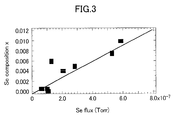
- Figure 3 shows the relationship between the actual selenium flux and the selenium content of the ZnOSe compound semiconductor.
- the above method of fabricating the light-emitting device makes it possible to introduce strain into the active layer by its ability to effect fine control of the content ratios of the zinc, magnesium, oxygen, selenium and sulfur in the upper and lower clad layers 5 and 3. This enables the realization of a semiconductor laser with a low threshold current to be expected.
- Figure 7 shows an example of a ZnOSSe semiconductor switching device according to the present invention, fabricated with a ZnOSSe layer 12 lattice-matched to the silicon substrate 11, with the ZnOSSe layer 12 being formed in a recessed portion 13 formed in the top face of the substrate.
- a positive electrode 14 is provided between the silicon substrate 11 and the ZnOSSe layer 12, and a negative electrode 15 is formed on the upper part of the ZnOSSe layer 12.
- the switching device of Figure 7 can be mounted on a silicon integrated circuit and can be used as an optical switching device with switching characteristics that change depending on the wavelength of the light concerned.
- the range can be selectively set from infrared and visible light to ultraviolet by changing the content ratios of the oxygen, selenium and sulfur components of the ZnOSSe layer 12, so that the device only functions when it receives light that is within the set wavelength region.
- the method of manufacturing the switching device and controlling the oxygen, selenium and sulfur content ratios is based on the method of manufacturing the light-emitting device described above.
- the ZnOSSe compound semiconductor of the present invention makes it possible to change the emission wavelength over a wide range that extends from infrared and visible light to ultraviolet light regions, simply by changing the mixture ratios of the oxygen, sulfur and selenium. Moreover, the ability to effect lattice-matching with the silicon substrate makes it possible to use it to fabricate optical devices capable of display, optical transmission and optical information processing on a silicon integrated circuit.
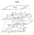
- FIG. 8 shows an example of an integrated circuit comprising a group of ZnOSSe semiconductor elements mounted on a silicon substrate.
- the integrated circuit comprises a SAW device 22 that includes input and output functions and a SAW oscillator, a ZnOSSe laser diode 23, a ZnOSSe photodetector 24, a ZnO FET 25, a ferroelectric memory 26, a microprocessor 27, a ZnOSSe SAW oscillator 28 and a SAW filter 29 that are mounted on a silicon substrate 21, to form an opto-electronic device.
- the method of manufacturing the integrated circuit is based on the method of manufacturing the light-emitting device described in the foregoing.
- the ZnOSSe semiconductor of the present invention can be lattice-matched to the silicon substrate and can therefore be provided on a silicon substrate together with conventional semiconductor device elements, making it possible to form wavelength multiplexing communication devices having a wide wavelength capability that ranges from infrared and visible light to ultraviolet light. This can be expected to facilitate a major downsizing of information terminals based on the convergence of information-processing and communication integrated circuits with display devices.
Landscapes
- Physics & Mathematics (AREA)
- Condensed Matter Physics & Semiconductors (AREA)
- General Physics & Mathematics (AREA)
- Electromagnetism (AREA)
- Optics & Photonics (AREA)
- Semiconductor Lasers (AREA)
- Led Devices (AREA)
- Crystals, And After-Treatments Of Crystals (AREA)
- Heterocyclic Carbon Compounds Containing A Hetero Ring Having Oxygen Or Sulfur (AREA)
- Semiconductor Integrated Circuits (AREA)
- Bipolar Transistors (AREA)
- Physical Deposition Of Substances That Are Components Of Semiconductor Devices (AREA)
Applications Claiming Priority (2)
| Application Number | Priority Date | Filing Date | Title |
|---|---|---|---|
| JP2001269497A JP4543162B2 (ja) | 2001-09-05 | 2001-09-05 | ZnOSSe混晶半導体 |
| JP2001269497 | 2001-09-05 |
Publications (3)
| Publication Number | Publication Date |
|---|---|
| EP1291930A2 true EP1291930A2 (de) | 2003-03-12 |
| EP1291930A3 EP1291930A3 (de) | 2007-05-09 |
| EP1291930B1 EP1291930B1 (de) | 2009-05-06 |
Family
ID=19095308
Family Applications (1)
| Application Number | Title | Priority Date | Filing Date |
|---|---|---|---|
| EP02256104A Expired - Lifetime EP1291930B1 (de) | 2001-09-05 | 2002-09-03 | ZnOSSe Halbleiterverbindung, integrierte Halbleiterschaltung und Verfahren zu deren Herstellung |
Country Status (5)
| Country | Link |
|---|---|
| US (1) | US6770913B2 (de) |
| EP (1) | EP1291930B1 (de) |
| JP (1) | JP4543162B2 (de) |
| AT (1) | ATE430992T1 (de) |
| DE (1) | DE60232213D1 (de) |
Cited By (2)
| Publication number | Priority date | Publication date | Assignee | Title |
|---|---|---|---|---|
| US7943927B2 (en) | 2007-01-15 | 2011-05-17 | Stanley Electric Co., Ltd. | ZnO based semiconductor light emitting device and its manufacture method |
| US8039867B2 (en) | 2007-02-27 | 2011-10-18 | Stanley Electric Co., Ltd. | ZnO-containing semiconductor layer, its manufacture method, and semiconductor light emitting device |
Families Citing this family (6)
| Publication number | Priority date | Publication date | Assignee | Title |
|---|---|---|---|---|
| DE10341681A1 (de) | 2003-09-08 | 2005-04-07 | TransMIT Gesellschaft für Technologietransfer mbH | Optische Funktionsschichten, insbesondere Zinkoxid-Sulfid-Schichten mit variabler dielektrischer Response |
| WO2008027896A2 (en) * | 2006-08-29 | 2008-03-06 | Moxtronics Inc. | Improved films and structures for metal oxide semiconductor light emitting devices and methods |
| JP5155611B2 (ja) * | 2007-07-06 | 2013-03-06 | スタンレー電気株式会社 | ZnO系半導体発光素子 |
| US8440497B2 (en) * | 2010-10-26 | 2013-05-14 | International Business Machines Corporation | Fabricating kesterite solar cells and parts thereof |
| US20120100663A1 (en) * | 2010-10-26 | 2012-04-26 | International Business Machines Corporation | Fabrication of CuZnSn(S,Se) Thin Film Solar Cell with Valve Controlled S and Se |
| US10121920B2 (en) * | 2015-06-30 | 2018-11-06 | International Business Machines Corporation | Aluminum-doped zinc oxysulfide emitters for enhancing efficiency of chalcogenide solar cell |
Family Cites Families (8)
| Publication number | Priority date | Publication date | Assignee | Title |
|---|---|---|---|---|
| JPH03160735A (ja) * | 1989-11-17 | 1991-07-10 | Daido Steel Co Ltd | 硫化亜鉛系化合物半導体 |
| US5045897A (en) * | 1990-03-14 | 1991-09-03 | Santa Barbara Research Center | Quaternary II-VI materials for photonics |
| US5838029A (en) * | 1994-08-22 | 1998-11-17 | Rohm Co., Ltd. | GaN-type light emitting device formed on a silicon substrate |
| JPH09219563A (ja) | 1996-02-09 | 1997-08-19 | Hitachi Ltd | 半導体光素子とそれを用いた応用システム |
| JPH09270564A (ja) * | 1996-04-01 | 1997-10-14 | Sony Corp | Ii−vi族化合物半導体の製造方法 |
| JPH11150337A (ja) * | 1997-11-14 | 1999-06-02 | Sony Corp | 半導体発光素子および光装置 |
| US6392257B1 (en) * | 2000-02-10 | 2002-05-21 | Motorola Inc. | Semiconductor structure, semiconductor device, communicating device, integrated circuit, and process for fabricating the same |
| JP2002016285A (ja) * | 2000-06-27 | 2002-01-18 | National Institute Of Advanced Industrial & Technology | 半導体発光素子 |
-
2001
- 2001-09-05 JP JP2001269497A patent/JP4543162B2/ja not_active Expired - Lifetime
-
2002
- 2002-09-03 EP EP02256104A patent/EP1291930B1/de not_active Expired - Lifetime
- 2002-09-03 AT AT02256104T patent/ATE430992T1/de not_active IP Right Cessation
- 2002-09-03 DE DE60232213T patent/DE60232213D1/de not_active Expired - Lifetime
- 2002-09-05 US US10/234,160 patent/US6770913B2/en not_active Expired - Fee Related
Cited By (2)
| Publication number | Priority date | Publication date | Assignee | Title |
|---|---|---|---|---|
| US7943927B2 (en) | 2007-01-15 | 2011-05-17 | Stanley Electric Co., Ltd. | ZnO based semiconductor light emitting device and its manufacture method |
| US8039867B2 (en) | 2007-02-27 | 2011-10-18 | Stanley Electric Co., Ltd. | ZnO-containing semiconductor layer, its manufacture method, and semiconductor light emitting device |
Also Published As
| Publication number | Publication date |
|---|---|
| JP4543162B2 (ja) | 2010-09-15 |
| EP1291930A3 (de) | 2007-05-09 |
| ATE430992T1 (de) | 2009-05-15 |
| JP2003081698A (ja) | 2003-03-19 |
| US6770913B2 (en) | 2004-08-03 |
| EP1291930B1 (de) | 2009-05-06 |
| DE60232213D1 (de) | 2009-06-18 |
| US20030042851A1 (en) | 2003-03-06 |
Similar Documents
| Publication | Publication Date | Title |
|---|---|---|
| US20170309781A1 (en) | Ultraviolet light-emitting devices incorporating graded layers and compositional offsets | |
| US20040079960A1 (en) | Semiconductor light emitting device and method for producing the same | |
| US20070126021A1 (en) | Metal oxide semiconductor film structures and methods | |
| EP0640248A1 (de) | Epitaktischer ohmscher Kontakt für integrierte Heterostruktur von II-VI-Halbleitermaterialien und Verfahren zu seiner Herstellung | |
| EP3509171A2 (de) | Oberflächenemittierende laservorrichtung und lichtemittierende vorrichtung damit | |
| WO2008027896A2 (en) | Improved films and structures for metal oxide semiconductor light emitting devices and methods | |
| US6770913B2 (en) | ZnOSSe compound semiconductor, integrated circuit using the semiconductor and method of manufacturing the semiconductor and the integrated circuit | |
| US6984850B2 (en) | Semiconductor light-emitting diode | |
| US20130234178A1 (en) | Semiconductor light emitting device and method for manufacturing the same | |
| US20090127572A1 (en) | Nitride Semiconductor Light Emitting Device | |
| EP2220694B1 (de) | Lichtemittierende vorrichtung mit angebundener schnittstelle | |
| US8699537B2 (en) | Application-oriented nitride substrates for epitaxial growth of electronic and optoelectronic device structures | |
| US20190207365A1 (en) | Semiconductor light-emitting element, manufacturing method of semiconductor light-emitting element, and semiconductor device | |
| US8030109B2 (en) | Semiconductor light emitting device, method of manufacturing same, and optical module | |
| KR102084067B1 (ko) | 표면발광 레이저 소자 및 이를 포함하는 발광장치 | |
| Grothe et al. | Influence of Mg doping on cutoff frequency and light output of InGaAsP/InP heterojunction LED's | |
| WO2003075365A1 (fr) | Dispositif de conversion photoelectrique | |
| TWI911536B (zh) | 半導體元件 | |
| JP7387048B1 (ja) | 半導体発光素子及び半導体発光素子の製造方法 | |
| CN111081836A (zh) | 发光二极管及其制造方法 | |
| JP7413599B1 (ja) | Iii-v族化合物半導体発光素子及びiii-v族化合物半導体発光素子の製造方法 | |
| JPS5929471A (ja) | 薄膜光導波路用基板 | |
| KR102515674B1 (ko) | 표면 광방출 레이저 소자 및 이를 포함하는 발광장치 | |
| CN121013518A (zh) | 半导体元件 | |
| WO2007067166A1 (en) | Metal oxide semiconductor devices and film structures and methods |
Legal Events
| Date | Code | Title | Description |
|---|---|---|---|
| PUAI | Public reference made under article 153(3) epc to a published international application that has entered the european phase |
Free format text: ORIGINAL CODE: 0009012 |
|
| AK | Designated contracting states |
Kind code of ref document: A2 Designated state(s): AT BE BG CH CY CZ DE DK EE ES FI FR GB GR IE IT LI LU MC NL PT SE SK TR Designated state(s): AT BE BG CH CY CZ DE DK EE ES FI FR GB GR IE IT LI LU MC NL PT SE SK TR |
|
| AX | Request for extension of the european patent |
Extension state: AL LT LV MK RO SI |
|
| PUAL | Search report despatched |
Free format text: ORIGINAL CODE: 0009013 |
|
| AK | Designated contracting states |
Kind code of ref document: A3 Designated state(s): AT BE BG CH CY CZ DE DK EE ES FI FR GB GR IE IT LI LU MC NL PT SE SK TR |
|
| AX | Request for extension of the european patent |
Extension state: AL LT LV MK RO SI |
|
| 17P | Request for examination filed |
Effective date: 20071018 |
|
| AKX | Designation fees paid |
Designated state(s): AT BE BG CH CY CZ DE DK EE ES FI FR GB GR IE IT LI LU MC NL PT SE SK TR |
|
| GRAP | Despatch of communication of intention to grant a patent |
Free format text: ORIGINAL CODE: EPIDOSNIGR1 |
|
| GRAS | Grant fee paid |
Free format text: ORIGINAL CODE: EPIDOSNIGR3 |
|
| GRAA | (expected) grant |
Free format text: ORIGINAL CODE: 0009210 |
|
| AK | Designated contracting states |
Kind code of ref document: B1 Designated state(s): AT BE BG CH CY CZ DE DK EE ES FI FR GB GR IE IT LI LU MC NL PT SE SK TR |
|
| REG | Reference to a national code |
Ref country code: GB Ref legal event code: FG4D |
|
| REG | Reference to a national code |
Ref country code: CH Ref legal event code: EP |
|
| REG | Reference to a national code |
Ref country code: IE Ref legal event code: FG4D |
|
| REF | Corresponds to: |
Ref document number: 60232213 Country of ref document: DE Date of ref document: 20090618 Kind code of ref document: P |
|
| PG25 | Lapsed in a contracting state [announced via postgrant information from national office to epo] |
Ref country code: PT Free format text: LAPSE BECAUSE OF FAILURE TO SUBMIT A TRANSLATION OF THE DESCRIPTION OR TO PAY THE FEE WITHIN THE PRESCRIBED TIME-LIMIT Effective date: 20090906 Ref country code: FI Free format text: LAPSE BECAUSE OF FAILURE TO SUBMIT A TRANSLATION OF THE DESCRIPTION OR TO PAY THE FEE WITHIN THE PRESCRIBED TIME-LIMIT Effective date: 20090506 Ref country code: ES Free format text: LAPSE BECAUSE OF FAILURE TO SUBMIT A TRANSLATION OF THE DESCRIPTION OR TO PAY THE FEE WITHIN THE PRESCRIBED TIME-LIMIT Effective date: 20090817 Ref country code: AT Free format text: LAPSE BECAUSE OF FAILURE TO SUBMIT A TRANSLATION OF THE DESCRIPTION OR TO PAY THE FEE WITHIN THE PRESCRIBED TIME-LIMIT Effective date: 20090506 |
|
| NLV1 | Nl: lapsed or annulled due to failure to fulfill the requirements of art. 29p and 29m of the patents act | ||
| PG25 | Lapsed in a contracting state [announced via postgrant information from national office to epo] |
Ref country code: SE Free format text: LAPSE BECAUSE OF FAILURE TO SUBMIT A TRANSLATION OF THE DESCRIPTION OR TO PAY THE FEE WITHIN THE PRESCRIBED TIME-LIMIT Effective date: 20090806 Ref country code: NL Free format text: LAPSE BECAUSE OF FAILURE TO SUBMIT A TRANSLATION OF THE DESCRIPTION OR TO PAY THE FEE WITHIN THE PRESCRIBED TIME-LIMIT Effective date: 20090506 |
|
| PG25 | Lapsed in a contracting state [announced via postgrant information from national office to epo] |
Ref country code: EE Free format text: LAPSE BECAUSE OF FAILURE TO SUBMIT A TRANSLATION OF THE DESCRIPTION OR TO PAY THE FEE WITHIN THE PRESCRIBED TIME-LIMIT Effective date: 20090506 Ref country code: DK Free format text: LAPSE BECAUSE OF FAILURE TO SUBMIT A TRANSLATION OF THE DESCRIPTION OR TO PAY THE FEE WITHIN THE PRESCRIBED TIME-LIMIT Effective date: 20090506 Ref country code: CZ Free format text: LAPSE BECAUSE OF FAILURE TO SUBMIT A TRANSLATION OF THE DESCRIPTION OR TO PAY THE FEE WITHIN THE PRESCRIBED TIME-LIMIT Effective date: 20090506 |
|
| PG25 | Lapsed in a contracting state [announced via postgrant information from national office to epo] |
Ref country code: SK Free format text: LAPSE BECAUSE OF FAILURE TO SUBMIT A TRANSLATION OF THE DESCRIPTION OR TO PAY THE FEE WITHIN THE PRESCRIBED TIME-LIMIT Effective date: 20090506 Ref country code: BE Free format text: LAPSE BECAUSE OF FAILURE TO SUBMIT A TRANSLATION OF THE DESCRIPTION OR TO PAY THE FEE WITHIN THE PRESCRIBED TIME-LIMIT Effective date: 20090506 |
|
| PLBE | No opposition filed within time limit |
Free format text: ORIGINAL CODE: 0009261 |
|
| STAA | Information on the status of an ep patent application or granted ep patent |
Free format text: STATUS: NO OPPOSITION FILED WITHIN TIME LIMIT |
|
| PG25 | Lapsed in a contracting state [announced via postgrant information from national office to epo] |
Ref country code: BG Free format text: LAPSE BECAUSE OF FAILURE TO SUBMIT A TRANSLATION OF THE DESCRIPTION OR TO PAY THE FEE WITHIN THE PRESCRIBED TIME-LIMIT Effective date: 20090806 |
|
| 26N | No opposition filed |
Effective date: 20100209 |
|
| PG25 | Lapsed in a contracting state [announced via postgrant information from national office to epo] |
Ref country code: MC Free format text: LAPSE BECAUSE OF NON-PAYMENT OF DUE FEES Effective date: 20090930 |
|
| REG | Reference to a national code |
Ref country code: CH Ref legal event code: PL |
|
| GBPC | Gb: european patent ceased through non-payment of renewal fee |
Effective date: 20090903 |
|
| REG | Reference to a national code |
Ref country code: FR Ref legal event code: ST Effective date: 20100531 |
|
| PG25 | Lapsed in a contracting state [announced via postgrant information from national office to epo] |
Ref country code: IE Free format text: LAPSE BECAUSE OF NON-PAYMENT OF DUE FEES Effective date: 20090903 Ref country code: FR Free format text: LAPSE BECAUSE OF NON-PAYMENT OF DUE FEES Effective date: 20090930 |
|
| PG25 | Lapsed in a contracting state [announced via postgrant information from national office to epo] |
Ref country code: LI Free format text: LAPSE BECAUSE OF NON-PAYMENT OF DUE FEES Effective date: 20090930 Ref country code: GR Free format text: LAPSE BECAUSE OF FAILURE TO SUBMIT A TRANSLATION OF THE DESCRIPTION OR TO PAY THE FEE WITHIN THE PRESCRIBED TIME-LIMIT Effective date: 20090807 Ref country code: CH Free format text: LAPSE BECAUSE OF NON-PAYMENT OF DUE FEES Effective date: 20090930 |
|
| PG25 | Lapsed in a contracting state [announced via postgrant information from national office to epo] |
Ref country code: GB Free format text: LAPSE BECAUSE OF NON-PAYMENT OF DUE FEES Effective date: 20090903 |
|
| PG25 | Lapsed in a contracting state [announced via postgrant information from national office to epo] |
Ref country code: IT Free format text: LAPSE BECAUSE OF FAILURE TO SUBMIT A TRANSLATION OF THE DESCRIPTION OR TO PAY THE FEE WITHIN THE PRESCRIBED TIME-LIMIT Effective date: 20090506 |
|
| PG25 | Lapsed in a contracting state [announced via postgrant information from national office to epo] |
Ref country code: LU Free format text: LAPSE BECAUSE OF NON-PAYMENT OF DUE FEES Effective date: 20090903 |
|
| PG25 | Lapsed in a contracting state [announced via postgrant information from national office to epo] |
Ref country code: TR Free format text: LAPSE BECAUSE OF FAILURE TO SUBMIT A TRANSLATION OF THE DESCRIPTION OR TO PAY THE FEE WITHIN THE PRESCRIBED TIME-LIMIT Effective date: 20090506 |
|
| PG25 | Lapsed in a contracting state [announced via postgrant information from national office to epo] |
Ref country code: CY Free format text: LAPSE BECAUSE OF FAILURE TO SUBMIT A TRANSLATION OF THE DESCRIPTION OR TO PAY THE FEE WITHIN THE PRESCRIBED TIME-LIMIT Effective date: 20090506 |
|
| PGFP | Annual fee paid to national office [announced via postgrant information from national office to epo] |
Ref country code: DE Payment date: 20110923 Year of fee payment: 10 |
|
| REG | Reference to a national code |
Ref country code: DE Ref legal event code: R119 Ref document number: 60232213 Country of ref document: DE Effective date: 20130403 |
|
| PG25 | Lapsed in a contracting state [announced via postgrant information from national office to epo] |
Ref country code: DE Free format text: LAPSE BECAUSE OF NON-PAYMENT OF DUE FEES Effective date: 20130403 |